

How Chiplet Integration Meets Industry Patenting Needs
OCT 15, 20259 MIN READ
Generate Your Research Report Instantly with AI Agent
Patsnap Eureka helps you evaluate technical feasibility & market potential.
Chiplet Technology Evolution and Objectives
Chiplet technology represents a paradigm shift in semiconductor design and manufacturing, evolving from traditional monolithic integrated circuits to a more modular approach. This evolution began in the early 2010s when semiconductor manufacturers faced increasing challenges with Moore's Law, as the economic and technical difficulties of shrinking transistors became more pronounced. The concept of disaggregating complex system-on-chip (SoC) designs into smaller, more manageable chiplets emerged as a viable solution to these challenges.
The evolution of chiplet technology can be traced through several key phases. Initially, the focus was on simple multi-chip modules (MCMs) that placed multiple dies side by side. This evolved into more sophisticated 2.5D integration using silicon interposers, exemplified by AMD's Fiji GPU in 2015. The current phase involves advanced packaging technologies like Intel's EMIB (Embedded Multi-die Interconnect Bridge) and TSMC's CoWoS (Chip on Wafer on Substrate), which enable high-bandwidth, low-latency connections between chiplets.
The primary objective of chiplet technology is to overcome the limitations of monolithic integration while maintaining performance advantages. By partitioning complex designs into smaller chiplets, manufacturers can optimize each component using the most appropriate process technology, thereby improving yield rates and reducing costs. This approach also enables the mixing of heterogeneous technologies, such as combining logic, memory, and analog components that would be difficult to integrate in a single monolithic design.
From a patenting perspective, chiplet technology presents unique objectives and challenges. Companies are increasingly focusing their patent strategies on interface standards, interconnect technologies, and system-level integration methods rather than just process technologies. The DARPA CHIPS program and industry consortia like UCIe (Universal Chiplet Interconnect Express) are working toward standardizing chiplet interfaces, which will significantly impact the patent landscape.
The future objectives of chiplet technology include achieving even higher integration densities through 3D stacking, developing more efficient thermal management solutions, and establishing industry-wide standards for chiplet interfaces. These advancements aim to enable a more modular and flexible approach to semiconductor design, potentially creating new business models where specialized chiplet providers can emerge alongside traditional integrated device manufacturers.
As the semiconductor industry continues to face scaling challenges, chiplet technology represents a critical path forward, with its evolution closely tied to the industry's ability to maintain performance improvements while managing increasing design complexity and manufacturing costs.
Market Demand Analysis for Chiplet Solutions
The global chiplet market is experiencing unprecedented growth, driven by the increasing demand for advanced computing solutions across various industries. As traditional monolithic chip designs reach their physical and economic limits, chiplet technology has emerged as a promising alternative that allows for more efficient and cost-effective semiconductor manufacturing. Market research indicates that the chiplet market is projected to grow at a compound annual growth rate of over 40% through 2026, reaching tens of billions of dollars in value.
This rapid market expansion is primarily fueled by the escalating computational requirements in data centers, artificial intelligence applications, and high-performance computing. Cloud service providers are particularly interested in chiplet solutions due to their ability to deliver customized performance while optimizing power consumption and reducing operational costs. The demand for chiplet-based processors in this sector alone is expected to double within the next three years.
Consumer electronics manufacturers are also driving significant demand for chiplet technology. As smartphones, tablets, and other personal devices continue to require more processing power while maintaining energy efficiency, chiplet integration offers an attractive solution. The automotive industry represents another growing market segment, with advanced driver-assistance systems and autonomous driving technologies requiring sophisticated computing capabilities that can benefit from chiplet architecture.
From a geographical perspective, North America and Asia-Pacific regions dominate the chiplet market demand. The United States leads in research and development initiatives, while Taiwan, South Korea, and China are rapidly expanding their manufacturing capabilities to meet the growing demand. European markets are showing increased interest, particularly in specialized applications for industrial automation and telecommunications infrastructure.
The patent landscape reflects this market demand, with a significant increase in chiplet-related patent filings over the past five years. Companies are strategically building patent portfolios around key chiplet technologies, including integration methods, interconnect standards, and testing methodologies. This patent activity indicates both the commercial value of chiplet solutions and the competitive nature of the market.
Industry surveys reveal that customers are primarily seeking chiplet solutions that address three key challenges: performance scaling, manufacturing yield improvement, and system integration flexibility. The ability to mix and match different process nodes and specialized functions within a single package is particularly valued by system designers looking to optimize their products for specific applications while managing development costs.
As market demand continues to grow, standardization efforts are becoming increasingly important. Customers are expressing strong interest in open chiplet ecosystems that would allow for greater interoperability between components from different vendors, potentially accelerating adoption and expanding the overall market opportunity.
Current Chiplet Integration Challenges
Chiplet integration faces several significant technical challenges that are shaping the industry's patenting landscape. The primary obstacle remains the development of standardized interfaces between chiplets from different manufacturers. Despite efforts from consortiums like UCIe (Universal Chiplet Interconnect Express), the industry still lacks fully established standards that enable seamless integration across vendor ecosystems, creating a fragmented patent environment where companies protect proprietary interconnect technologies.
The manufacturing complexity of chiplet-based systems presents another major challenge. The precise alignment and bonding of multiple chiplets require advanced packaging technologies such as 2.5D and 3D integration. These processes involve sophisticated thermal management solutions and mechanical stress mitigation techniques, all of which are becoming hotly contested areas for patent filings as companies seek to protect their manufacturing innovations.
Testing and validation methodologies for multi-chiplet systems represent a growing technical hurdle. Traditional testing approaches designed for monolithic chips are insufficient for detecting defects at chiplet interfaces or addressing system-level performance issues. This has spurred a new wave of patents focused on novel testing protocols and equipment specifically designed for chiplet architectures.
Power management across chiplet boundaries introduces unique challenges that conventional approaches cannot adequately address. The need for efficient power delivery networks and dynamic power management systems that can optimize performance across heterogeneous chiplets has led to increased patenting activity in power distribution architectures and management algorithms.
Signal integrity and latency issues between chiplets remain persistent technical problems. As data rates increase, maintaining signal quality across chiplet interfaces becomes increasingly difficult, particularly when dealing with high-bandwidth applications. Companies are aggressively patenting solutions for signal conditioning, equalization techniques, and novel interconnect materials to overcome these limitations.
The design tool ecosystem for chiplet-based systems is still evolving, with significant gaps in capabilities for multi-vendor chiplet integration. EDA (Electronic Design Automation) companies are racing to patent new methodologies for chiplet-based system simulation, verification, and optimization that can handle the complexity of heterogeneous integration.
Security concerns present another dimension of challenges, as chiplet architectures introduce new attack surfaces at the interfaces between components. This has prompted increased patent activity around secure chiplet authentication mechanisms, encrypted interfaces, and hardware-based security features designed specifically for multi-chiplet environments.
Current Chiplet Integration Approaches
01 Advanced Interconnect Technologies for Chiplet Integration
Various interconnect technologies are employed to facilitate communication between chiplets in multi-die systems. These include through-silicon vias (TSVs), micro-bumps, and hybrid bonding techniques that enable high-bandwidth, low-latency connections between chiplets. Advanced packaging technologies like 2.5D and 3D integration allow for vertical stacking or side-by-side placement of chiplets on interposers, enhancing system performance while reducing form factors.- Advanced Interconnect Technologies for Chiplet Integration: Various interconnect technologies are being developed to enable efficient chiplet integration. These include advanced packaging methods like silicon interposers, organic substrates, and through-silicon vias (TSVs) that facilitate high-bandwidth, low-latency communication between chiplets. These interconnect solutions address the challenges of signal integrity, power delivery, and thermal management in multi-chiplet systems, allowing for higher performance and more efficient heterogeneous integration.
- Heterogeneous Integration of Chiplets: Heterogeneous integration involves combining chiplets manufactured using different process technologies or having different functionalities into a single package. This approach allows for optimizing each component separately, combining memory, logic, analog, and RF components manufactured at their ideal process nodes. The integration enables system designers to mix and match chiplets from different vendors, potentially reducing costs and development time while improving overall system performance and power efficiency.
- Thermal Management Solutions for Chiplet Designs: Effective thermal management is crucial for chiplet-based systems due to the high power densities and potential hotspots at interconnect points. Various cooling solutions are being developed, including integrated heat spreaders, microchannel cooling, and advanced thermal interface materials specifically designed for chiplet architectures. These thermal management techniques help maintain optimal operating temperatures across multiple chiplets with different power profiles, ensuring reliability and consistent performance.
- Design and Testing Methodologies for Chiplet-Based Systems: Specialized design and testing methodologies are emerging to address the unique challenges of chiplet-based systems. These include new EDA tools for chiplet-aware design, pre-silicon validation techniques, and post-integration testing approaches. Standards and protocols are being developed to ensure interoperability between chiplets from different vendors. These methodologies help manage the increased complexity of chiplet-based designs and ensure reliable operation of the integrated system.
- Power Delivery and Management for Chiplet Integration: Power delivery and management present significant challenges in chiplet integration due to the diverse power requirements of different chiplets and the need for efficient power distribution across interconnects. Advanced power delivery networks, integrated voltage regulators, and power management techniques are being developed specifically for chiplet architectures. These solutions aim to optimize power efficiency while maintaining performance, addressing issues such as voltage droop, power integrity, and dynamic power management across multiple integrated chiplets.
02 Thermal Management Solutions for Chiplet Architectures
Effective thermal management is critical in chiplet-based designs due to high power densities and heat concentration. Solutions include integrated heat spreaders, thermal interface materials, and advanced cooling techniques such as liquid cooling or microfluidic channels. These approaches help maintain optimal operating temperatures across multiple chiplets, preventing thermal throttling and ensuring reliable performance in high-performance computing applications.Expand Specific Solutions03 Power Delivery Networks for Multi-Chiplet Systems
Specialized power delivery networks are designed to provide stable and efficient power distribution across multiple chiplets. These include integrated voltage regulators, power management ICs, and advanced power distribution architectures that minimize voltage droop and power loss. Techniques such as point-of-load regulation and dynamic voltage scaling help optimize power efficiency while meeting the diverse power requirements of heterogeneous chiplets.Expand Specific Solutions04 Heterogeneous Integration of Chiplets
Heterogeneous integration combines chiplets manufactured using different process technologies or from different vendors into a single package. This approach allows for optimizing each component for its specific function, such as combining high-performance logic chiplets with specialized accelerators, memory, or analog components. Advanced die-to-die interfaces and standardized protocols enable seamless communication between diverse chiplets, maximizing overall system performance and efficiency.Expand Specific Solutions05 Design and Testing Methodologies for Chiplet-Based Systems
Specialized design tools and testing methodologies are developed to address the unique challenges of chiplet-based systems. These include pre-silicon validation techniques, known-good-die testing, and post-assembly verification methods to ensure functionality and reliability. Design automation tools support chiplet-specific considerations such as die-to-die interface optimization, system-level power and thermal analysis, and yield management strategies to improve manufacturing economics.Expand Specific Solutions
Key Industry Players in Chiplet Ecosystem
Chiplet integration technology is currently in a growth phase, with the market expanding rapidly due to increasing demand for heterogeneous computing solutions. The global chiplet market is projected to grow significantly as semiconductor companies seek more efficient alternatives to monolithic designs. From a technical maturity perspective, industry leaders like TSMC, Intel, and AMD have made substantial advancements in chiplet architecture and integration methods, with TSMC's advanced packaging technologies and Intel's EMIB and Foveros technologies representing significant innovations. Micron and SK hynix are contributing memory-specific chiplet solutions, while Huawei and OPPO are developing mobile applications. The competitive landscape shows established semiconductor giants investing heavily alongside specialized players like AvicenaTech focusing on optical interconnects for chiplets, indicating a diversifying ecosystem with varying levels of patent activity across different integration approaches.
Taiwan Semiconductor Manufacturing Co., Ltd.
Technical Solution: TSMC has developed its Chip-on-Wafer-on-Substrate (CoWoS) and Integrated Fan-Out (InFO) technologies as cornerstone chiplet integration platforms. CoWoS uses silicon interposers to connect multiple chiplets with thousands of interconnections, while InFO embeds chips in a reconstituted wafer for improved thermal performance and form factor. TSMC has significantly expanded its patent portfolio in advanced packaging, focusing on high-density interconnect technologies, interposer designs, and manufacturing processes for multi-chip modules. Their SoIC (System on Integrated Chips) technology further advances 3D integration with sub-micron connections between stacked dies. TSMC's approach emphasizes standardization of interfaces and manufacturing processes to enable their diverse customer base to leverage chiplet designs while protecting their IP through strategic patenting of critical manufacturing processes rather than specific chip designs.
Strengths: Industry-leading process technology; extensive manufacturing experience; broad ecosystem of partners using their technologies. Weaknesses: Higher cost for silicon interposer solutions; thermal challenges in densely stacked configurations; dependency on partners for complete system design.
Intel Corp.
Technical Solution: Intel has pioneered chiplet integration through its EMIB (Embedded Multi-die Interconnect Bridge) and Foveros 3D packaging technologies. EMIB uses silicon bridges embedded in the package substrate to connect multiple chiplets with high-bandwidth, short-reach connections. This approach enables high-density interconnects between adjacent chiplets without the cost of full silicon interposers. Intel's Foveros technology extends this to true 3D integration, stacking compute tiles vertically with through-silicon vias (TSVs). Intel has built a substantial patent portfolio around these technologies, with particular focus on die-to-die interfaces, power delivery mechanisms across chiplets, and thermal management solutions. Their Ponte Vecchio GPU demonstrates the commercial application of this approach, combining over 40 tiles manufactured on different process nodes into a single package, showcasing their advanced heterogeneous integration capabilities.
Strengths: Mature manufacturing infrastructure; extensive patent portfolio covering both 2D and 3D integration; proven commercial implementations. Weaknesses: Proprietary interconnect standards may limit industry adoption; higher manufacturing complexity compared to monolithic designs; thermal challenges in densely packed multi-die products.
Core Patents and Technical Innovations
Edge interface placements to enable chiplet rotation into multi-chiplet cluster
PatentWO2022119635A9
Innovation
- The solution involves arranging multiple blocks of I/O pads on the edges of chiplets symmetrically relative to the centerline, allowing for rotation to achieve correct alignment and close-coupled interconnects, thereby facilitating dense packaging and minimizing the system footprint.
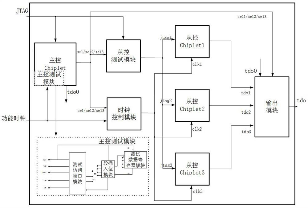
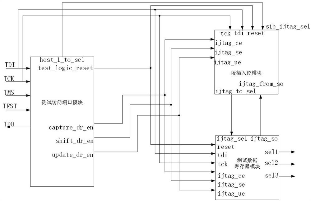
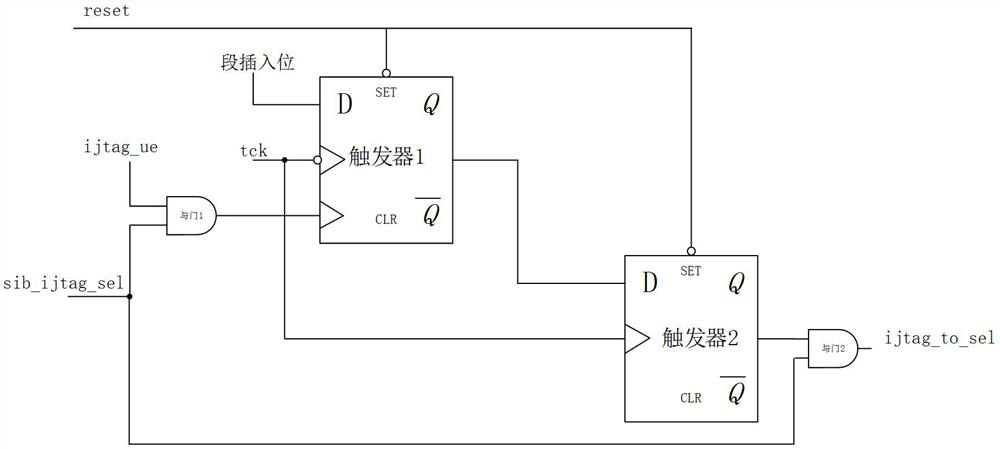
Controllable Chiplet serial test circuit
PatentActiveCN114578217A
Innovation
- A controllable Chiplet serial test circuit using a master-slave architecture generates control signals through the master test module, and only uses 5 JTAG ports to test all Chiplets one by one to achieve serial testing and ensure the independence and non-influence between Chiplets.
IP Protection Strategies for Chiplet Technology
The protection of intellectual property in chiplet technology presents unique challenges due to the modular nature of these systems. As chiplet integration becomes increasingly prevalent in semiconductor manufacturing, companies must develop comprehensive IP protection strategies that address the multi-vendor ecosystem inherent to this approach.
Patent portfolios for chiplet technologies should focus on three critical areas: interface standards, integration methodologies, and system-level innovations. Companies investing in chiplet development need to secure patents covering both the individual chiplets and the integration technologies that enable their functionality as a cohesive system. This dual-layer protection approach helps safeguard innovations across the entire technology stack.
Cross-licensing agreements have emerged as a vital component of chiplet IP strategies. These agreements allow multiple companies to share protected technologies while maintaining competitive advantages. The Universal Chiplet Interconnect Express (UCIe) consortium exemplifies this collaborative approach, where industry leaders have established shared standards while preserving proprietary implementations.
Trade secret protection complements patent strategies, particularly for manufacturing processes and integration techniques that may be difficult to reverse-engineer. Companies must implement robust internal security protocols to prevent knowledge leakage, especially when collaborating with external partners in the chiplet supply chain.
Defensive publication represents another strategic tool in the chiplet IP landscape. By publicly disclosing certain innovations without patenting them, companies can prevent competitors from obtaining exclusive rights while maintaining freedom to operate. This approach is particularly valuable for incremental improvements that may not warrant full patent protection.
International IP protection considerations are essential given the global nature of semiconductor supply chains. Companies must navigate varying patent laws across jurisdictions, particularly in regions with significant semiconductor manufacturing capacity such as Taiwan, South Korea, and the United States.
Open-source approaches are gaining traction in specific segments of chiplet technology. RISC-V based chiplets, for example, leverage open hardware principles while companies build proprietary extensions and integration technologies around these cores. This hybrid model balances innovation sharing with competitive differentiation.
The development of IP monitoring systems has become necessary to track potential infringement in the complex chiplet ecosystem. Advanced analytics and AI-powered patent monitoring tools help companies identify potential IP conflicts early and inform strategic decision-making regarding licensing, litigation, or design modifications.
Standardization Efforts in Chiplet Integration
The standardization landscape for chiplet integration has evolved significantly in recent years, driven by the need for interoperability and patent protection strategies. Key industry consortia like the Universal Chiplet Interconnect Express (UCIe) have emerged as critical forces in establishing common frameworks for chiplet-to-chiplet communication. UCIe's standardization efforts focus on physical layer, protocol stack, and software abstraction layers, creating a comprehensive ecosystem that enables chiplets from different vendors to work seamlessly together.
JEDEC and Open Compute Project (OCP) have also contributed substantially to the standardization ecosystem, with JEDEC focusing on memory interface standards critical for chiplet integration, while OCP promotes open-source hardware designs that incorporate chiplet technologies. These standardization bodies create patent-friendly environments where companies can innovate while adhering to industry-accepted norms.
The Chiplet Design Exchange (CDX) represents another significant standardization initiative, establishing common design methodologies and verification procedures. This framework enables companies to protect their intellectual property while participating in the broader chiplet ecosystem, addressing a critical concern in patent strategy development.
From a patenting perspective, these standardization efforts create strategic opportunities through Standard Essential Patents (SEPs). Companies actively participating in standard development can position their innovations as essential to implementation, potentially generating licensing revenue streams. The standardization process itself often requires participants to declare relevant patents and commit to Fair, Reasonable, and Non-Discriminatory (FRAND) licensing terms, creating a balanced ecosystem for innovation.
Geographically, standardization efforts show interesting patterns with North American companies leading UCIe initiatives, while Asian manufacturers contribute significantly to implementation standards. European entities often focus on specialized interface standards and testing methodologies, creating a globally distributed standardization landscape that reflects regional technological strengths.
The timeline of standardization shows acceleration, with early fragmented efforts from 2018-2020 giving way to more coordinated industry-wide initiatives from 2021 onward. This consolidation trend suggests the industry recognizes that fragmented standards would impede chiplet adoption and complicate patent landscapes, driving competitors toward collaborative standardization despite potential patent conflicts.
Looking forward, emerging standardization efforts are focusing on thermal management interfaces, testing protocols, and security frameworks for chiplet integration. These developing standards represent new frontiers for patent development and strategic positioning as the chiplet ecosystem continues to mature.
Unlock deeper insights with Patsnap Eureka Quick Research — get a full tech report to explore trends and direct your research. Try now!
Generate Your Research Report Instantly with AI Agent
Supercharge your innovation with Patsnap Eureka AI Agent Platform!