

Exploring Comparative Analysis: Chiplet Integration vs Alternatives
OCT 15, 20259 MIN READ
Generate Your Research Report Instantly with AI Agent
Patsnap Eureka helps you evaluate technical feasibility & market potential.
Chiplet Technology Evolution and Objectives
The evolution of semiconductor technology has been marked by continuous advancements in integration and performance enhancement. Since the introduction of Moore's Law in 1965, the industry has pursued relentless miniaturization of transistors to increase computational density. However, as process nodes approach physical limits, traditional monolithic integration faces mounting challenges in terms of yield, cost, and design complexity. This technological inflection point has catalyzed the emergence of chiplet architecture as a promising alternative to conventional system-on-chip (SoC) designs.
Chiplet technology represents a paradigm shift from monolithic integration to a more modular approach, where complex systems are disaggregated into smaller functional blocks manufactured separately and then integrated using advanced packaging technologies. The concept originated in the early 2010s but gained significant momentum around 2017 when major semiconductor companies began implementing chiplet-based designs in commercial products. This evolution was driven by the need to overcome the limitations of traditional scaling while maintaining performance improvements and cost efficiency.
The primary objective of chiplet technology is to enable continued scaling of system performance and functionality beyond what is achievable through traditional monolithic integration. By partitioning complex systems into smaller dies, manufacturers can optimize each component using the most appropriate process technology, thereby maximizing performance while minimizing costs. Additionally, chiplet architecture aims to improve yield rates by reducing the size of individual dies, as smaller dies statistically encounter fewer defects during fabrication.
Another critical objective is to enhance design flexibility and reusability. Chiplet-based approaches allow companies to mix and match pre-validated functional blocks across different products, significantly reducing development time and engineering resources. This modular approach also facilitates heterogeneous integration, combining components with different process technologies, materials, or even from different manufacturers within a single package.
The evolution trajectory of chiplet technology has been characterized by progressive improvements in interconnect technologies, from through-silicon vias (TSVs) to more advanced approaches like silicon interposers and direct copper-to-copper bonding. These advancements have been crucial in addressing the bandwidth, latency, and power consumption challenges associated with inter-die communication, which represents one of the fundamental technical hurdles in chiplet implementation.
Looking forward, the chiplet ecosystem is evolving toward standardization of interfaces and protocols to enable a more open marketplace for chiplet components. Industry consortia such as UCIe (Universal Chiplet Interconnect Express) are working to establish common specifications that would allow chiplets from different vendors to be seamlessly integrated, potentially revolutionizing the semiconductor supply chain and business models.
Market Demand Analysis for Chiplet Solutions
The global semiconductor market is witnessing a significant shift towards chiplet-based architectures, driven by increasing demand for higher performance, improved power efficiency, and cost-effective scaling solutions. Market research indicates that the chiplet technology market is projected to grow at a compound annual growth rate of 40% between 2023 and 2030, reaching approximately 50 billion dollars by the end of the decade. This remarkable growth trajectory underscores the industry's recognition of chiplets as a viable alternative to traditional monolithic designs.
The primary market demand for chiplet solutions stems from data centers and high-performance computing sectors, where the need for processing power continues to escalate exponentially. These segments currently account for nearly 45% of the total chiplet market share, with telecommunications and consumer electronics following closely behind. The demand is particularly strong in applications requiring specialized accelerators for artificial intelligence and machine learning workloads, where chiplets offer the flexibility to combine different process nodes and IP blocks.
Enterprise customers are increasingly seeking chiplet solutions to address the limitations of traditional monolithic designs, particularly as Moore's Law faces economic and physical constraints. A recent survey of semiconductor procurement managers revealed that 78% of large technology companies are evaluating chiplet-based architectures for their next-generation products, citing performance gains and supply chain resilience as key motivating factors.
From a geographical perspective, North America and East Asia dominate the chiplet market demand, collectively representing over 70% of global consumption. However, emerging markets in Europe and South Asia are showing accelerated adoption rates, particularly in automotive and industrial applications where chiplets offer advantages in terms of reliability and specialized functionality integration.
The market demand is further characterized by industry-specific requirements. Cloud service providers are prioritizing chiplet solutions that maximize compute density and memory bandwidth, while edge computing applications favor designs that optimize power efficiency and thermal management. The automotive sector, meanwhile, is increasingly interested in chiplets that can meet stringent reliability standards while enabling advanced driver assistance systems and autonomous driving capabilities.
Supply chain considerations are also driving demand for chiplet solutions. The semiconductor shortage of 2020-2022 highlighted vulnerabilities in traditional monolithic approaches, prompting many OEMs to explore disaggregated designs that offer greater flexibility in sourcing components from multiple suppliers. This trend is expected to continue, with 65% of semiconductor industry executives identifying supply chain resilience as a key factor in their technology roadmap decisions.
Current Chiplet Integration Challenges
Despite the promising advantages of chiplet architecture, the industry faces several significant technical challenges that impede widespread adoption and optimal implementation. The foremost challenge lies in the interconnect technology between chiplets. Current solutions like silicon interposers and organic substrates present trade-offs between performance, cost, and manufacturing complexity. Silicon interposers offer excellent electrical characteristics but remain expensive and difficult to manufacture at scale, while organic substrates are more cost-effective but suffer from lower interconnect density and signal integrity issues.
Thermal management represents another critical challenge in chiplet integration. As multiple dies are packed closely together, heat dissipation becomes increasingly problematic. The thermal interface materials between chiplets and heat spreaders often create bottlenecks in heat transfer, leading to potential hotspots and thermal throttling. This challenge is particularly acute in high-performance computing applications where power densities continue to rise.
Known-good-die (KGD) testing presents a significant manufacturing hurdle. Unlike traditional monolithic designs where testing occurs after complete assembly, chiplet architectures require comprehensive pre-integration testing of individual dies. Current testing methodologies are not fully optimized for chiplet-specific requirements, resulting in yield and reliability concerns that increase overall production costs.
Power delivery network (PDN) design across multiple chiplets introduces complex engineering challenges. Maintaining consistent power delivery across different dies with varying power requirements demands sophisticated PDN architectures. Voltage droop and power integrity issues can arise at chiplet interfaces, potentially compromising system stability and performance.
Design and verification methodologies for multi-chiplet systems remain immature compared to traditional SoC approaches. The industry lacks standardized tools and workflows specifically tailored for chiplet-based designs. Engineers must navigate complex trade-offs between chiplet partitioning, interface optimization, and system-level performance considerations without well-established design frameworks.
Standardization represents perhaps the most significant ecosystem challenge. Despite initiatives like UCIe (Universal Chiplet Interconnect Express), the industry still lacks comprehensive standards for chiplet interfaces, protocols, and physical design. This fragmentation impedes the development of a truly open chiplet ecosystem where dies from different vendors can be seamlessly integrated, limiting the potential for market growth and innovation in heterogeneous integration.
Memory integration and bandwidth optimization between chiplets continue to present performance bottlenecks, particularly as data-intensive applications drive demand for higher memory bandwidth and lower latency solutions.
Comparative Analysis of Integration Approaches
01 Advanced Interconnect Technologies for Chiplet Integration
Various interconnect technologies are being developed to enable efficient chiplet integration. These include advanced packaging methods, through-silicon vias (TSVs), and high-bandwidth interconnects that facilitate communication between different chiplets. These technologies aim to minimize signal latency, reduce power consumption, and enhance overall system performance by optimizing the connections between integrated chiplets.- Interconnect technologies for chiplet integration: Various interconnect technologies are used to enable communication between chiplets in multi-die packages. These include advanced micro-bumps, through-silicon vias (TSVs), and silicon interposers that facilitate high-bandwidth, low-latency connections between chiplets. These interconnect solutions address challenges related to signal integrity, power delivery, and thermal management while enabling high-performance data transfer between integrated chiplets.
- Packaging architectures for chiplet integration: Different packaging architectures support chiplet integration, including 2.5D and 3D integration approaches. These architectures involve stacking or placing chiplets side by side on interposers or substrates. Advanced packaging technologies such as fan-out wafer-level packaging (FOWLP) and embedded multi-die interconnect bridge (EMIB) enable heterogeneous integration of chiplets with different process technologies, optimizing performance, power efficiency, and form factor.
- Thermal management solutions for chiplet designs: Thermal management is critical in chiplet integration due to high power densities and heat generation. Solutions include integrated heat spreaders, thermal interface materials, and advanced cooling techniques such as microfluidic cooling channels. These approaches help maintain optimal operating temperatures across multiple chiplets, preventing thermal throttling and ensuring reliability and performance consistency in densely packed multi-die packages.
- Power delivery networks for chiplet architectures: Specialized power delivery networks are designed to supply stable power to multiple chiplets in integrated systems. These include advanced voltage regulators, power distribution architectures, and integrated capacitors that minimize power noise and voltage droop. Efficient power delivery is essential for maintaining performance and reliability across chiplets with different power requirements and operating conditions.
- Design and testing methodologies for chiplet systems: Specialized design and testing methodologies are developed for chiplet-based systems to ensure functionality and reliability. These include design-for-test approaches, known-good-die testing, and post-integration validation techniques. Advanced EDA tools support chiplet-based design flows, addressing challenges in signal integrity, timing closure, and system-level verification across multiple dies from potentially different vendors or process technologies.
02 Thermal Management Solutions for Chiplet Architectures
Effective thermal management is crucial for chiplet-based systems due to the high power density and heat generation. Innovations in this area include advanced cooling techniques, thermal interface materials, and heat dissipation structures specifically designed for multi-chiplet packages. These solutions help maintain optimal operating temperatures, prevent thermal throttling, and ensure reliability of chiplet-integrated systems under various workloads.Expand Specific Solutions03 Heterogeneous Integration of Chiplets
Heterogeneous integration involves combining chiplets manufactured using different process technologies or having different functionalities into a single package. This approach allows for optimizing each component separately while achieving system-level performance benefits. The integration methods include 2.5D and 3D packaging technologies that enable mixing of memory, logic, analog, and other specialized chiplets to create highly customized and efficient computing solutions.Expand Specific Solutions04 Testing and Yield Improvement for Chiplet-Based Systems
Testing methodologies and yield improvement techniques specific to chiplet-based designs are being developed to ensure reliability and cost-effectiveness. These include pre-integration testing protocols, known-good-die strategies, and built-in self-test mechanisms for individual chiplets and their interconnections. Advanced testing approaches help identify defects early in the manufacturing process, improving overall yield and reducing costs in chiplet-based system production.Expand Specific Solutions05 Design Automation and Standards for Chiplet Integration
Design automation tools and standardization efforts are emerging to facilitate chiplet-based system development. These include specialized EDA tools for chiplet-based designs, interface standards for chiplet communication, and design methodologies that support modular integration. Standardization initiatives aim to create an ecosystem where chiplets from different vendors can be seamlessly integrated, promoting wider adoption of chiplet-based architectures across the semiconductor industry.Expand Specific Solutions
Key Industry Players in Chiplet Ecosystem
Chiplet integration technology is currently in the growth phase of its industry lifecycle, with a rapidly expanding market projected to reach significant scale by 2030. The competitive landscape features established semiconductor giants like Intel, TSMC, and AMD leading commercial implementation, while Qualcomm and IBM advance research initiatives. These companies are leveraging chiplet technology to overcome monolithic chip scaling limitations and improve manufacturing yields. Technical maturity varies across players, with Intel's EMIB and TSMC's CoWoS platforms representing more mature solutions, while newer entrants like Huawei and Micron are developing proprietary approaches. The ecosystem is evolving toward standardization through initiatives like UCIe, with specialized players like Avicena Tech emerging to address specific interconnect challenges in the chiplet architecture paradigm.
Intel Corp.
Technical Solution: Intel's chiplet integration approach centers around their Advanced Interface Bus (AIB) and Embedded Multi-die Interconnect Bridge (EMIB) technologies. EMIB enables high-density connections between chiplets without requiring expensive silicon interposers, using small silicon bridges embedded in the package substrate instead. This allows Intel to mix and match different process nodes and IP blocks efficiently. Their Foveros 3D packaging technology further extends chiplet capabilities by stacking dies vertically. Intel's Ponte Vecchio GPU demonstrates this approach with over 47 tiles manufactured on multiple process nodes and connected via EMIB and Foveros. Their latest Meteor Lake processors utilize chiplet design with separate compute, graphics, I/O, and AI tiles manufactured at different nodes, showcasing the practical implementation of their disaggregated approach to chip design.
Strengths: Intel's approach offers flexibility in mixing different process technologies, reducing costs compared to monolithic designs while maintaining high bandwidth connections. Their mature packaging technologies enable heterogeneous integration of specialized components. Weaknesses: Their proprietary interconnect standards may limit ecosystem adoption compared to more open alternatives, and their packaging technologies add complexity to the manufacturing process, potentially affecting yields.
Taiwan Semiconductor Manufacturing Co., Ltd.
Technical Solution: TSMC has developed advanced chiplet integration technologies centered around their Integrated Fan-Out (InFO) and System on Integrated Chips (SoIC) platforms. Their CoWoS (Chip-on-Wafer-on-Substrate) technology uses silicon interposers to connect multiple chiplets with thousands of interconnections at much higher density than traditional package-level integration. TSMC's SoIC technology enables both chip-on-wafer and wafer-on-wafer bonding with extremely fine pitch connections (less than 10 microns), allowing for true 3D integration of chiplets. Their latest 3DFabric technology combines frontend and backend innovations to support various chiplet integration approaches. TSMC has demonstrated bandwidth of over 2 TB/s between chiplets using their advanced packaging, while reducing power consumption by up to 30% compared to traditional designs. Their technology supports both homogeneous integration (same process node chiplets) and heterogeneous integration across different process technologies.
Strengths: TSMC offers industry-leading interconnect density and bandwidth between chiplets, with proven high-volume manufacturing capabilities. Their open ecosystem approach allows multiple customers to leverage their packaging technologies. Weaknesses: Their advanced packaging solutions like CoWoS use expensive silicon interposers, increasing costs, and their most advanced integration technologies have limited availability due to high demand and manufacturing complexity.
Critical Patents and Research in Chiplet Design
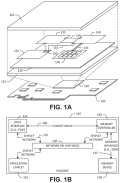
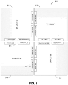
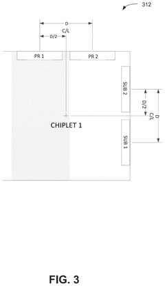
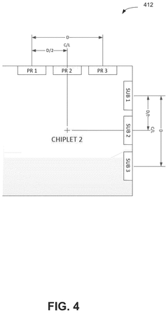
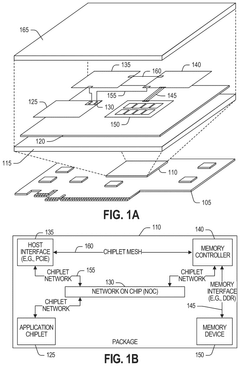
Edge interface placements to enable chiplet rotation into multi-chiplet cluster
PatentActiveUS20240332257A1
Innovation
- The implementation of a chiplet architecture that uses a network-on-chip (NOC) with a chiplet protocol interface (CPI) to facilitate high-speed, flexible inter-chiplet communication, combined with a tightly packed matrix arrangement of chiplets and I/O micro-bumps for close-coupled interconnects, allowing for proper alignment and minimal footprint.
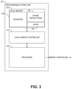
Detecting infinite loops in a programmable atomic transaction
PatentActiveUS20240311149A1
Innovation
- Implementing a method within the programmable atomic unit to detect and terminate programmable atomic transactions that exceed a predetermined instruction execution limit, using an instruction counter to monitor execution and send a response to the calling processor if the limit is reached, thereby freeing resources and preventing system stalls.
Cost-Performance Tradeoffs
The economic considerations of chiplet integration versus monolithic designs present a complex landscape of tradeoffs that significantly impact both manufacturers and end-users. When evaluating chiplet architecture against traditional monolithic approaches, manufacturing costs emerge as a primary differentiator. Chiplet designs typically demonstrate superior yield rates, as smaller dies inherently experience fewer defects during production. This yield advantage translates to approximately 15-25% cost reduction for high-complexity systems compared to equivalent monolithic implementations.
However, the cost equation must account for additional factors unique to chiplet integration. The packaging technologies required for chiplet implementation—such as advanced interposers, silicon bridges, or organic substrates—introduce supplementary expenses ranging from $20-100 per unit depending on complexity. Furthermore, the testing procedures for chiplet-based systems demand more sophisticated protocols to verify inter-die communication integrity, potentially adding 5-10% to overall validation costs.
Performance considerations create another dimension in this analysis. Chiplet architectures typically introduce latency penalties of 3-15 nanoseconds for inter-die communication compared to on-die connections in monolithic designs. This latency impact varies significantly based on the specific integration technology employed, with silicon interposers offering superior performance but at higher cost than organic substrates. Power efficiency presents a similar tradeoff, with chiplet designs consuming approximately 5-8% additional power for communication infrastructure.
The economic calculus shifts dramatically when considering time-to-market advantages. Chiplet approaches enable parallel development of different functional blocks, potentially reducing development cycles by 30-40% compared to monolithic equivalents. This acceleration creates substantial competitive advantages in rapidly evolving markets and can significantly enhance return on investment despite potentially higher unit costs.
Scale considerations further complicate this analysis. For high-volume production exceeding millions of units, the initial tooling and design costs of chiplet integration become increasingly amortized, enhancing cost competitiveness. Conversely, for specialized applications with limited production volumes, the higher fixed costs of chiplet design may outweigh manufacturing yield benefits, favoring monolithic approaches despite their technical limitations.
The long-term economic perspective must also consider product lifecycle management. Chiplet architectures offer superior upgradeability, potentially extending product lifespans by allowing selective component replacement rather than complete system redesigns. This modularity can reduce total ownership costs by 15-30% over multiple product generations, particularly for enterprise and infrastructure applications where deployment longevity is prioritized.
Standardization Efforts and Interoperability
The standardization landscape for chiplet integration has evolved significantly in recent years, with several industry consortia and organizations working to establish common frameworks. The Universal Chiplet Interconnect Express (UCIe) consortium, formed in 2022, represents a major milestone in these efforts, bringing together key industry players including Intel, AMD, Arm, TSMC, and Samsung. UCIe aims to establish an open industry standard for die-to-die interconnects, focusing on physical layer, protocol stack, and software definitions to enable chiplets from different vendors to work together seamlessly.
Parallel to UCIe, the Open Compute Project (OCP) has been advancing the Open Domain-Specific Architecture (ODSA) subproject, which focuses on creating open interfaces and standards for chiplet-based systems. The ODSA has developed several key specifications including the Bunch of Wires (BoW) interface and Chiplet Design Exchange (CDX) format, addressing both physical interconnection and design exchange challenges.
JEDEC and IEEE have also contributed significantly to standardization efforts, with JEDEC focusing on memory interface standards critical for chiplet integration, and IEEE working on broader system-level standards that impact chiplet implementation. These organizations provide the formal standardization processes necessary to move industry consortia proposals into widely adopted standards.
Interoperability remains a central challenge in chiplet integration. Current efforts focus on three key areas: physical interconnects, protocols, and software stacks. Physical interconnect standardization addresses signal integrity, power delivery, and thermal management across chiplet boundaries. Protocol standardization ensures consistent communication methods between chiplets, while software stack standardization enables operating systems and applications to effectively utilize multi-chiplet architectures.
Testing and validation frameworks represent another critical aspect of interoperability. Organizations like DMTF (Distributed Management Task Force) are developing standards for chiplet validation and compliance testing, ensuring that chiplets from different vendors can be certified for interoperability.
The economic implications of standardization are substantial. A 2023 analysis by Yole Development suggests that standardized chiplet interfaces could reduce integration costs by 25-40% compared to proprietary solutions, while accelerating time-to-market by up to 50%. This economic incentive has accelerated industry participation in standardization efforts, with over 80 companies now actively contributing to various chiplet standards.
Unlock deeper insights with Patsnap Eureka Quick Research — get a full tech report to explore trends and direct your research. Try now!
Generate Your Research Report Instantly with AI Agent
Supercharge your innovation with Patsnap Eureka AI Agent Platform!