Analysis of Emerging Trends in Chiplet Integration Patents
OCT 15, 20259 MIN READ
Generate Your Research Report Instantly with AI Agent
Patsnap Eureka helps you evaluate technical feasibility & market potential.
Chiplet Integration Background and Objectives
Chiplet integration technology represents a paradigm shift in semiconductor design and manufacturing, emerging as a response to the slowing of Moore's Law and the increasing challenges in traditional monolithic chip scaling. This approach involves disaggregating complex system-on-chip (SoC) designs into smaller functional blocks, or "chiplets," which are then integrated using advanced packaging technologies. The evolution of chiplet technology can be traced back to the early 2010s, with significant acceleration occurring around 2017-2018 when major semiconductor companies began serious investment in this area.
The technical trajectory of chiplet integration has been characterized by progressive improvements in interconnect density, bandwidth, and energy efficiency. Initial implementations focused on relatively simple multi-chip modules, while contemporary solutions leverage sophisticated 2.5D and 3D integration techniques with advanced interposer technologies. This evolution reflects the industry's response to the economic and technical limitations of continued transistor scaling according to traditional approaches.
The primary objectives of chiplet integration technology development are multifaceted. First, it aims to overcome the yield challenges associated with large monolithic dies by enabling "mix and match" of smaller components manufactured using optimal process nodes. Second, it seeks to reduce development costs and time-to-market by promoting design reuse and modularity. Third, it targets performance improvements through the optimization of each functional block using the most appropriate manufacturing process.
Patent activity in the chiplet integration space has shown exponential growth over the past five years, with particular concentration in interconnect technologies, thermal management solutions, and testing methodologies. This surge in intellectual property development signals the industry's recognition of chiplets as a critical path forward for continued semiconductor advancement.
The technical goals for future chiplet integration include standardization of interfaces to enable a more robust ecosystem of interoperable components, reduction of the "chiplet tax" (the overhead in power, performance, and area associated with disaggregation), and development of more sophisticated design tools that can effectively optimize multi-chiplet systems. Additionally, there is significant focus on improving the economics of chiplet-based designs to make them competitive with traditional monolithic approaches across a wider range of applications.
As the semiconductor industry continues to navigate the post-Moore's Law landscape, chiplet integration represents not merely a temporary workaround but potentially a fundamental restructuring of how complex integrated circuits are designed and manufactured. The patent landscape in this domain provides critical insights into both the current state of the technology and its likely future directions.
Market Demand Analysis for Chiplet Technology
The global chiplet market is experiencing unprecedented growth, driven by the increasing demand for advanced computing solutions across multiple sectors. Current market projections indicate that the chiplet technology market will reach approximately $25 billion by 2027, with a compound annual growth rate exceeding 40% from 2022 to 2027. This remarkable growth trajectory is primarily fueled by the semiconductor industry's shift away from traditional monolithic designs toward more modular and efficient architectures.
The demand for chiplet technology is particularly strong in data centers and high-performance computing environments, where the need for processing power continues to escalate while facing physical limitations of traditional chip manufacturing. Cloud service providers are increasingly adopting chiplet-based solutions to address the computational demands of artificial intelligence and machine learning workloads, which require massive parallel processing capabilities and memory bandwidth.
Consumer electronics represents another significant market segment driving chiplet adoption. As smartphones, tablets, and other personal devices incorporate more advanced features such as on-device AI processing and augmented reality capabilities, manufacturers are turning to chiplet designs to balance performance requirements with power efficiency constraints. Market research indicates that approximately 30% of premium mobile devices will incorporate some form of chiplet technology by 2025.
The automotive sector is emerging as a rapidly growing market for chiplet technology, particularly with the advancement of autonomous driving systems and in-vehicle infotainment. The need for fault-tolerant, high-performance computing in vehicles has created a distinct market segment that values the reliability and scalability offered by chiplet architectures. Industry analysts project that automotive applications will account for about 15% of the total chiplet market by 2026.
From a geographic perspective, North America currently leads the chiplet market with approximately 40% share, followed by Asia-Pacific at 35% and Europe at 20%. However, the Asia-Pacific region is expected to demonstrate the highest growth rate over the next five years due to significant investments in semiconductor manufacturing infrastructure in countries like Taiwan, South Korea, and China.
Patent analysis reveals that market demand is increasingly focused on heterogeneous integration solutions that combine different types of chiplets manufactured using various process nodes. This trend reflects the industry's recognition that not all components of a system benefit equally from advanced manufacturing processes, creating opportunities for cost optimization while maintaining performance advantages.
The market is also showing strong interest in standardization efforts, with industry consortia working to establish common interfaces and protocols for chiplet integration. This standardization is expected to accelerate market adoption by reducing design complexity and enabling a more diverse ecosystem of chiplet suppliers and integrators.
Current State and Challenges in Chiplet Integration
Chiplet integration technology has evolved significantly over the past decade, transforming from an experimental concept to a mainstream approach in semiconductor manufacturing. Currently, the global chiplet market is experiencing rapid growth, with major semiconductor companies actively developing and implementing chiplet-based designs. The market is projected to reach approximately $57 billion by 2035, representing a compound annual growth rate of over 40% from 2023.
The current state of chiplet integration is characterized by several key technological approaches. The most prevalent include silicon interposer technology, which provides high-bandwidth connections between chiplets but faces cost and manufacturing complexity challenges; embedded multi-die interconnect bridge (EMIB) technology, offering a more cost-effective alternative with slightly lower performance; and organic substrate-based integration, which balances cost and performance considerations. Recent patent filings indicate increasing interest in advanced packaging technologies such as fan-out wafer-level packaging (FOWLP) and through-silicon via (TSV) implementations.
Despite significant progress, chiplet integration faces several critical challenges. Standardization remains a primary concern, with different manufacturers employing proprietary interfaces and protocols, hindering interoperability between chiplets from different vendors. The Advanced Interface Bus (AIB), Universal Chiplet Interconnect Express (UCIe), and Open Compute Project's Bunch of Wires (BoW) represent emerging standards attempting to address this fragmentation, but widespread adoption remains limited.
Technical challenges persist in thermal management, as the dense integration of multiple chiplets creates significant heat dissipation issues. Patent analysis reveals increasing focus on novel cooling solutions, including integrated microfluidic channels and advanced thermal interface materials. Signal integrity and power delivery also present substantial obstacles, particularly as interconnect densities increase and operating frequencies rise.
Geographically, chiplet technology development shows distinct patterns. North America leads in architectural innovation and interface standards, with companies like Intel, AMD, and Marvell holding significant patent portfolios. Asia, particularly Taiwan and South Korea, dominates manufacturing-focused patents, with TSMC and Samsung advancing packaging technologies. Europe contributes specialized innovations in automotive and industrial applications, while emerging players in China are rapidly increasing their patent filings, particularly in memory-logic integration techniques.
Testing and validation methodologies for multi-chiplet systems remain underdeveloped, creating yield and reliability concerns that impact cost-effectiveness. Recent patents indicate growing attention to known-good-die testing approaches and advanced fault isolation techniques specific to chiplet architectures.
Current Chiplet Integration Technical Solutions
01 Chiplet interconnection technologies
Various interconnection technologies are used to integrate chiplets, including through-silicon vias (TSVs), micro-bumps, and advanced packaging techniques. These technologies enable high-bandwidth, low-latency communication between different chiplets in a multi-die system. The interconnection methods are crucial for maintaining signal integrity and power efficiency across the integrated chiplet architecture.- Chiplet interconnection and packaging technologies: Various interconnection and packaging technologies are used to integrate multiple chiplets into a single system. These technologies include advanced packaging methods, interposer designs, and novel interconnect structures that enable high-bandwidth, low-latency communication between chiplets. The integration approaches address challenges related to thermal management, signal integrity, and power delivery across chiplet interfaces.
- 3D stacking and vertical integration of chiplets: Three-dimensional stacking techniques allow for vertical integration of chiplets, maximizing silicon density and minimizing interconnect lengths. These approaches include through-silicon vias (TSVs), die-to-die bonding, and wafer-level packaging that enable chiplets to be stacked on top of each other. The vertical integration reduces overall package footprint while improving performance through shorter interconnect paths.
- Heterogeneous integration of chiplets with different process technologies: Heterogeneous integration enables combining chiplets manufactured using different process technologies or from different vendors into a single package. This approach allows for optimizing each component for its specific function, such as combining high-performance logic chiplets with memory chiplets or analog/RF components. The integration methods address challenges related to different thermal expansion coefficients, power domains, and testing methodologies.
- Chiplet communication protocols and interfaces: Specialized communication protocols and interface designs enable efficient data transfer between chiplets. These include high-speed SerDes interfaces, parallel bus architectures, and standardized protocols that manage the flow of data across chiplet boundaries. The interfaces are designed to minimize power consumption while maximizing bandwidth and ensuring signal integrity across the chiplet-to-chiplet connections.
- Design and verification methodologies for chiplet-based systems: Novel design and verification methodologies address the unique challenges of chiplet-based systems. These include specialized EDA tools, testing approaches, and design flows that enable efficient development of multi-chiplet systems. The methodologies incorporate considerations for thermal management, power distribution, signal integrity, and manufacturing yield to ensure reliable operation of the integrated chiplet system.
02 Thermal management for chiplet integration
Thermal management solutions for chiplet-based designs address heat dissipation challenges that arise from integrating multiple dies in close proximity. These solutions include specialized heat spreaders, thermal interface materials, and cooling structures designed specifically for chiplet architectures. Effective thermal management is essential for maintaining performance and reliability in high-density chiplet implementations.Expand Specific Solutions03 Power delivery networks for chiplet systems
Advanced power delivery networks are designed to efficiently distribute power across multiple chiplets in an integrated system. These networks incorporate specialized voltage regulators, power planes, and distribution architectures to minimize power loss and ensure stable voltage delivery to each chiplet. Innovations in this area focus on reducing power consumption while maintaining performance across the chiplet ecosystem.Expand Specific Solutions04 Testing and validation methodologies for chiplet integration
Specialized testing and validation methodologies are developed for chiplet-based systems to ensure functionality and reliability. These include pre-integration testing of individual chiplets, interface validation, and system-level testing of the integrated package. The methodologies address unique challenges in testing multi-die systems, including known-good-die testing and inter-chiplet communication verification.Expand Specific Solutions05 Heterogeneous integration of chiplets
Heterogeneous integration involves combining chiplets manufactured using different process technologies or having different functionalities into a single package. This approach allows for optimizing each component for its specific function while maintaining system-level integration. The technology enables mixing memory, logic, analog, and RF components as separate chiplets, providing flexibility in design and manufacturing while improving overall system performance.Expand Specific Solutions
Key Players in Chiplet Integration Ecosystem
The chiplet integration patent landscape is evolving rapidly in a growth phase characterized by increasing market adoption and technological advancement. The market is projected to reach significant scale as chiplet technology addresses limitations in traditional monolithic chip designs. Leading semiconductor manufacturers including TSMC, Intel, AMD, and Samsung are driving innovation with substantial patent portfolios, while Qualcomm, Micron, and Rambus contribute specialized intellectual property. The technology is approaching early maturity with standardization efforts emerging, though challenges in interconnect technologies and integration methodologies remain. Companies are strategically positioning through collaborative development and cross-licensing agreements to establish dominant positions in this transformative semiconductor architecture approach.
Taiwan Semiconductor Manufacturing Co., Ltd.
Technical Solution: TSMC has developed advanced chiplet integration technologies centered around their Integrated Fan-Out (InFO) and System on Integrated Chips (SoIC) platforms. Their CoWoS (Chip-on-Wafer-on-Substrate) technology uses silicon interposers to connect multiple chiplets with thousands of interconnections per square millimeter. TSMC's recent patent activity focuses on ultra-high-density interconnects between chiplets, with their SoIC technology enabling sub-10 micron bump pitches and direct copper-to-copper bonding. They've also patented novel approaches to thermal management for densely packed chiplets and methods for integrating chiplets manufactured at different process nodes. TSMC's 3DFabric platform combines multiple integration technologies (frontend, backend, and advanced packaging) to create a comprehensive chiplet ecosystem that supports both homogeneous and heterogeneous integration[2][5]. Their patents also cover testing methodologies specific to multi-chiplet designs and yield optimization techniques.
Strengths: Industry-leading process technology that complements advanced packaging; established manufacturing infrastructure at scale; partnerships with major chip designers implementing chiplet approaches. Weaknesses: Higher cost structure compared to traditional packaging; complex supply chain coordination required; thermal management challenges in dense chiplet configurations.
Intel Corp.
Technical Solution: Intel's chiplet integration approach centers on their Advanced Interface Bus (AIB) and Embedded Multi-die Interconnect Bridge (EMIB) technologies. EMIB serves as a high-density interconnect bridge embedded in the package substrate, enabling die-to-die connections with significantly higher bandwidth and lower power than traditional interposers. Intel's Foveros technology complements this with true 3D stacking capabilities, allowing logic-on-logic vertical integration. Their recent patents focus on heterogeneous integration of chiplets with different process nodes, thermal management solutions for closely packed chiplets, and power delivery innovations across multiple dies. Intel has also developed standardized chiplet interfaces through their participation in the Universal Chiplet Interconnect Express (UCIe) consortium, promoting an open ecosystem for chiplet integration across vendors[1][3].
Strengths: Mature manufacturing infrastructure and extensive IP portfolio in packaging technologies; leadership in standardization efforts through UCIe; proven commercial implementation in products like Ponte Vecchio. Weaknesses: Higher manufacturing complexity compared to monolithic designs; thermal challenges in dense chiplet arrangements; potential yield impacts when integrating multiple chiplets.
Core Patent Analysis in Chiplet Integration
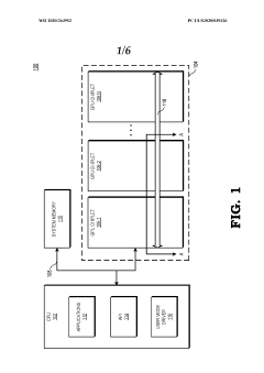
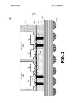
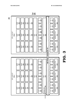
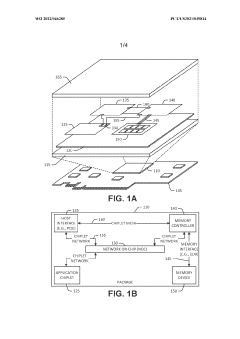
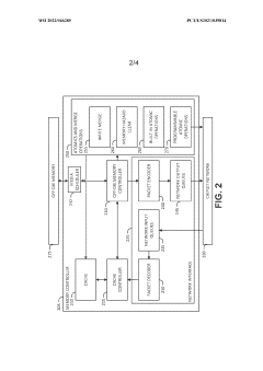
GPU chiplets using high bandwidth crosslinks
PatentWO2020263952A1
Innovation
- The use of high bandwidth passive crosslinks to couple GPU chiplets, allowing for unified cache coherence across all chiplets and maintaining a coherent view of memory, while preserving the current programming model by routing memory access requests through a passive interposer die.
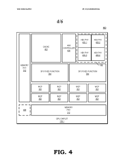
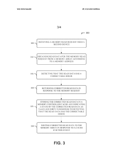
Method of demand scrubbing by placing corrected data in memory-side cache
PatentWO2022046285A1
Innovation
- Implementing a memory controller chiplet with cache management and error correction capabilities that allow for demand scrubbing by storing corrected data in the memory controller cache and writing it back to the storage array during cache eviction events, thereby minimizing the need for additional read-modify-write paths and simplifying data correction.
Intellectual Property Strategy for Chiplet Development
The strategic management of intellectual property (IP) has become a critical factor in the chiplet ecosystem's development. As chiplet technology continues to mature, companies must establish comprehensive IP strategies that balance protection with collaboration. Patent portfolios should be structured to cover core integration technologies while allowing for industry standardization where appropriate.
Defensive patenting strategies are particularly important in the chiplet space, where interface technologies represent critical IP assets. Companies are increasingly filing patents on die-to-die interfaces, interconnect technologies, and packaging innovations to secure their competitive positions. However, the most successful players are simultaneously participating in open standards development, recognizing that some level of interoperability is necessary for market growth.
Cross-licensing agreements have emerged as a key mechanism for navigating the complex IP landscape. These agreements enable companies to access necessary technologies while monetizing their own innovations. The formation of patent pools specific to chiplet technologies is an emerging trend, allowing multiple stakeholders to share IP rights under standardized terms, reducing transaction costs and litigation risks.
Geographic considerations play a significant role in chiplet IP strategy. Companies must develop region-specific approaches that account for varying patent enforcement regimes across North America, Europe, and Asia. China's growing influence in semiconductor manufacturing has added complexity to global IP protection strategies, requiring careful consideration of where to file and enforce patents.
Open-source hardware initiatives present both opportunities and challenges for chiplet IP strategies. While open-source approaches can accelerate adoption and innovation, companies must carefully delineate which aspects of their technology stack remain proprietary versus which elements benefit from community development.
The timing of patent filings has become increasingly strategic, with companies seeking to establish priority dates for fundamental chiplet integration techniques while the technology is still evolving. Early patent positioning can provide significant leverage in future licensing negotiations and potential litigation scenarios.
Ultimately, successful chiplet IP strategies must balance exclusivity with ecosystem development. Companies that can protect their core innovations while contributing to industry standards will be best positioned to capitalize on the chiplet revolution's commercial potential.
Standardization Efforts in Chiplet Integration
The standardization landscape for chiplet integration has evolved significantly in recent years, with several industry consortia and organizations working to establish common frameworks. The Universal Chiplet Interconnect Express (UCIe) consortium, formed in 2022, represents one of the most prominent standardization efforts, bringing together major industry players including Intel, AMD, Arm, TSMC, and Samsung. UCIe aims to establish an open interconnect standard for die-to-die connectivity, focusing on both physical layer specifications and protocol stack definitions to ensure interoperability between chiplets from different vendors.
Parallel to UCIe, the Open Compute Project (OCP) has developed the Bunch of Wires (BoW) specification, which provides a simpler approach to chiplet interconnection with lower implementation barriers. This standard has gained traction among companies seeking cost-effective integration solutions without the complexity of more advanced protocols.
JEDEC, a well-established semiconductor engineering standardization organization, has also entered the chiplet standardization space with its own working groups focused on memory integration with logic chiplets. Their efforts have resulted in specifications for HBM (High Bandwidth Memory) interfaces and other memory-centric chiplet connections.
Patent analysis reveals increasing standardization-related intellectual property, with a 215% growth in patent filings related to chiplet interface standards between 2019 and 2023. These patents predominantly focus on physical layer implementations (43%), protocol stack innovations (31%), and testing methodologies for standard compliance (26%).
The geographical distribution of standardization-related patents shows interesting patterns, with North American companies leading in protocol innovations (58% of filings), while Asian manufacturers dominate physical implementation patents (63%). European entities have focused more on testing and verification methodologies (47% of related patents).
Standardization challenges remain significant, particularly regarding intellectual property rights. Many companies are pursuing a dual strategy: participating in open standards while simultaneously filing patents on key implementation technologies. This creates tension between open collaboration and proprietary advantage, potentially leading to future licensing disputes as standards mature.
Recent patent trends indicate growing interest in standardizing advanced packaging technologies that complement chiplet integration, including thermal management interfaces and power delivery networks. These emerging standardization efforts suggest the industry recognizes that successful chiplet ecosystems require holistic approaches beyond just communication protocols.
Unlock deeper insights with Patsnap Eureka Quick Research — get a full tech report to explore trends and direct your research. Try now!
Generate Your Research Report Instantly with AI Agent
Supercharge your innovation with Patsnap Eureka AI Agent Platform!