

Exploring Chiplet Integration in Emerging Market Applications
OCT 15, 202510 MIN READ
Generate Your Research Report Instantly with AI Agent
Patsnap Eureka helps you evaluate technical feasibility & market potential.
Chiplet Technology Background and Objectives
Chiplet technology represents a paradigm shift in semiconductor design and manufacturing, evolving from traditional monolithic System-on-Chip (SoC) approaches to a more modular and flexible architecture. This evolution began in the mid-2010s as semiconductor manufacturers faced increasing challenges with Moore's Law, particularly regarding yield, cost, and design complexity at advanced nodes. The fundamental concept involves disaggregating complex SoCs into smaller functional blocks (chiplets) that can be manufactured separately and then integrated using advanced packaging technologies.
The historical trajectory of chiplet development shows acceleration since 2017, with AMD's introduction of their Infinity Fabric interconnect technology in Ryzen processors marking a significant commercial milestone. Intel followed with their Embedded Multi-die Interconnect Bridge (EMIB) and Foveros technologies, while TSMC developed their Integrated Fan-Out (InFO) and System on Integrated Chips (SoIC) solutions. These developments have established chiplets as a viable alternative to traditional monolithic designs.
Current technical objectives for chiplet integration in emerging markets focus on several key areas. First is the standardization of chiplet interfaces, with initiatives like Universal Chiplet Interconnect Express (UCIe) consortium working to establish industry-wide protocols for chiplet-to-chiplet communication. This standardization aims to create an ecosystem where chiplets from different vendors can be seamlessly integrated, similar to how USB standardized peripheral connections.
Another critical objective is reducing the power and latency penalties associated with inter-chiplet communication. Current solutions still face efficiency challenges compared to monolithic designs, particularly for applications with stringent power constraints like mobile devices and IoT endpoints. Research is actively pursuing advanced packaging technologies that can minimize these penalties.
Cost optimization represents another significant goal, as current advanced packaging technologies remain expensive compared to traditional approaches. For chiplets to penetrate emerging markets beyond high-performance computing, packaging costs must decrease substantially while maintaining reliability and performance.
The miniaturization of chiplet integration technologies is also crucial for emerging applications in wearables, medical devices, and edge computing. Current packaging solutions often require considerable space, limiting their applicability in highly constrained form factors.
Finally, thermal management presents a substantial challenge, particularly as chiplet designs enable higher compute densities. Developing effective cooling solutions that work across heterogeneous chiplet assemblies remains a key research area, especially for emerging applications in autonomous vehicles, industrial IoT, and next-generation mobile devices where operating environments can be unpredictable and harsh.
Market Demand Analysis for Chiplet Solutions
The chiplet market is experiencing unprecedented growth driven by several converging factors. As traditional monolithic chip designs reach their physical and economic limits, chiplet architecture has emerged as a compelling alternative that offers improved yield, cost efficiency, and design flexibility. Current market analysis indicates that the global chiplet market, valued at approximately $5.8 billion in 2023, is projected to reach $47.2 billion by 2030, representing a compound annual growth rate (CAGR) of 34.8%.
This remarkable growth trajectory is fueled by escalating demand across multiple sectors. In data centers and cloud computing environments, the need for high-performance, energy-efficient processors has never been greater. These facilities require solutions that can handle increasingly complex workloads while minimizing power consumption and heat generation. Chiplets address these challenges by enabling heterogeneous integration of specialized components optimized for specific functions.
The telecommunications sector, particularly with the ongoing global 5G rollout and preparation for 6G technologies, represents another significant market driver. Network infrastructure requires advanced processing capabilities to manage the exponential increase in data traffic and edge computing demands. Chiplet-based solutions offer the performance density and power efficiency necessary for next-generation communication systems.
Consumer electronics manufacturers are increasingly turning to chiplet technology to differentiate their products in a competitive marketplace. The ability to rapidly integrate various functional blocks—such as AI accelerators, graphics processors, and specialized I/O—allows for more customized solutions that better meet specific application requirements while maintaining competitive pricing.
Automotive applications represent one of the fastest-growing segments for chiplet technology. Advanced driver-assistance systems (ADAS), autonomous driving capabilities, and in-vehicle infotainment all demand sophisticated computing solutions that can operate reliably in challenging environmental conditions. The modularity of chiplet designs allows automotive manufacturers to scale computing resources appropriately while maintaining strict safety and reliability standards.
Market research indicates that approximately 78% of semiconductor companies are either already implementing or actively exploring chiplet-based designs. This industry-wide shift is creating new ecosystem dynamics, with specialized providers emerging for individual chiplet components, integration technologies, and testing methodologies.
Regional analysis shows North America currently leading the chiplet market with approximately 42% share, followed by Asia-Pacific at 38% and Europe at 16%. However, the Asia-Pacific region is expected to demonstrate the highest growth rate over the next five years, driven by substantial investments in semiconductor manufacturing infrastructure and strong government support for technological advancement in countries like Taiwan, South Korea, and China.
Current Chiplet Integration Challenges
Despite the promising advancements in chiplet technology, significant integration challenges persist that impede widespread adoption across emerging markets. The primary technical hurdle remains the development of standardized interfaces between chiplets from different vendors. Current proprietary interfaces like Intel's AIB, AMD's Infinity Fabric, and TSMC's LIPINCON create ecosystem fragmentation, preventing true mix-and-match capabilities that would accelerate innovation in smaller market segments.
Thermal management presents another critical challenge, particularly for high-performance applications in resource-constrained environments. The dense packaging of multiple chiplets creates concentrated heat zones that require sophisticated cooling solutions, often beyond what is economically viable for emerging market applications. This thermal barrier becomes especially problematic when considering deployment in regions with limited infrastructure or extreme climate conditions.
Testing and validation methodologies for multi-chiplet systems remain underdeveloped compared to monolithic designs. The complexity increases exponentially with each additional chiplet, as interconnect pathways, signal integrity, and power distribution must be verified across numerous die-to-die interfaces. This complexity translates to higher development costs that can be prohibitive for smaller market segments or applications with moderate performance requirements.
Manufacturing yield considerations continue to impact chiplet economics. While chiplet approaches theoretically improve overall yield by using smaller dies, the additional processing steps for advanced packaging can introduce new failure modes. The testing infrastructure required to identify known-good-die before integration adds cost layers that can offset the yield advantages, particularly for lower-volume applications typical in emerging markets.
Supply chain complexity represents a significant non-technical barrier. Coordinating multiple vendors for different chiplets, packaging technologies, and testing protocols introduces logistical challenges and potential bottlenecks. This complexity is particularly problematic for emerging market applications where supply chain resilience may already be compromised by regional infrastructure limitations.
Power management across multiple chiplets with varying process technologies presents unique design challenges. The heterogeneous nature of chiplet-based systems requires sophisticated power delivery networks and management algorithms to optimize performance while maintaining efficiency. This challenge becomes particularly acute in battery-powered or energy-constrained applications common in emerging markets.
Security considerations for multi-chiplet systems introduce additional complexity. The increased number of physical interfaces between components creates potential attack surfaces that must be secured. Establishing trust between chiplets from different vendors remains an evolving challenge that requires industry-wide standards and protocols still under development.
Current Chiplet Integration Methodologies
01 Interconnect technologies for chiplet integration
Various interconnect technologies are used to connect multiple chiplets in a single package. These include advanced micro-bump technologies, through-silicon vias (TSVs), and bridge interconnects that enable high-bandwidth, low-latency communication between chiplets. These interconnect solutions address challenges related to signal integrity, power delivery, and thermal management while facilitating high-density integration of heterogeneous chiplets.- Chiplet interconnection technologies: Various interconnection technologies are used to integrate chiplets, including advanced packaging methods that enable high-bandwidth, low-latency communication between different chiplets. These technologies include silicon interposers, organic substrates, and direct bonding techniques that facilitate the connection of heterogeneous chiplets manufactured using different process nodes. The interconnection architecture is crucial for maintaining performance while allowing modular design approaches.
- Thermal management in chiplet integration: Thermal management is a critical aspect of chiplet integration as the dense packaging of multiple dies can lead to heat concentration issues. Solutions include integrated cooling systems, thermal interface materials, and strategic placement of chiplets to optimize heat dissipation. Advanced thermal management techniques help maintain performance and reliability of chiplet-based systems while preventing thermal throttling under high computational loads.
- Power delivery optimization for chiplet designs: Efficient power delivery is essential in chiplet-based architectures to ensure stable operation across multiple integrated dies. This involves specialized power distribution networks, voltage regulation techniques, and power management systems that can address the varying power requirements of heterogeneous chiplets. Advanced power delivery solutions help minimize power loss while maintaining signal integrity across chiplet interfaces.
- Testing and validation methodologies for chiplet systems: Testing integrated chiplet systems presents unique challenges compared to monolithic designs. Specialized methodologies have been developed for pre-integration testing of individual chiplets, as well as post-integration validation of the complete system. These approaches include built-in self-test circuits, boundary scan techniques, and advanced probe technologies that enable comprehensive testing while maintaining manufacturing efficiency and yield rates.
- Design automation and standardization for chiplet ecosystems: The development of design automation tools and standardized interfaces is crucial for the widespread adoption of chiplet technology. This includes EDA tools specifically designed for multi-chiplet systems, standardized protocols for chiplet communication, and design methodologies that facilitate the integration of chiplets from different vendors. These advancements support the creation of a chiplet ecosystem where components can be mixed and matched to create customized semiconductor solutions.
02 Packaging technologies for chiplet integration
Advanced packaging technologies play a crucial role in chiplet integration, including 2.5D and 3D packaging approaches. These technologies involve stacking chiplets vertically or placing them side by side on an interposer. The packaging solutions address thermal management challenges, provide mechanical support, and facilitate electrical connections between chiplets while enabling higher integration density and improved system performance.Expand Specific Solutions03 Design methodologies for chiplet-based systems
Specialized design methodologies are essential for developing chiplet-based systems. These include partitioning strategies to divide system functionality across multiple chiplets, standardized interfaces to ensure compatibility between chiplets from different vendors, and design-for-test approaches specific to multi-chiplet architectures. These methodologies help manage complexity, optimize performance, and ensure reliable operation of integrated chiplet systems.Expand Specific Solutions04 Heterogeneous integration of chiplets
Heterogeneous integration involves combining chiplets manufactured using different process technologies or having different functionalities into a single package. This approach allows for optimizing each component using the most suitable manufacturing process while maintaining high performance and energy efficiency. It enables the integration of logic, memory, analog, and RF components as separate chiplets to create highly specialized and efficient systems.Expand Specific Solutions05 Thermal management solutions for chiplet integration
Effective thermal management is critical for chiplet-based systems due to high power density and potential hotspots. Solutions include integrated heat spreaders, thermal interface materials specifically designed for chiplet architectures, liquid cooling systems, and thermal-aware placement of chiplets. These approaches help maintain optimal operating temperatures, prevent thermal throttling, and ensure reliability and longevity of chiplet-based systems.Expand Specific Solutions
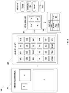
Key Industry Players in Chiplet Ecosystem
Chiplet integration is currently in the early growth phase, with the market expanding rapidly as semiconductor companies seek more efficient alternatives to monolithic designs. The global chiplet market is projected to reach significant scale by 2030, driven by increasing demand for high-performance computing and AI applications. Technology maturity varies across players, with industry leaders like TSMC, Intel, and AMD demonstrating advanced capabilities in chiplet design and integration. TSMC leads in manufacturing processes, while Intel's EMIB and AMD's Infinity Fabric represent mature interconnect technologies. Qualcomm and Micron are advancing memory-centric chiplet solutions, while emerging players like AvicenaTech are developing innovative optical interconnect technologies. Research institutions including Tsinghua University and IMEC are contributing fundamental advancements, indicating a collaborative ecosystem developing around this transformative approach to semiconductor design.
Taiwan Semiconductor Manufacturing Co., Ltd.
Technical Solution: TSMC has developed advanced chiplet integration technologies including Integrated Fan-Out (InFO), Chip on Wafer on Substrate (CoWoS), and System on Integrated Chips (SoIC). Their CoWoS platform enables high-bandwidth connections between multiple chiplets on a silicon interposer, supporting up to 12 high-bandwidth memory (HBM) stacks and multiple compute dies. TSMC's 3DFabric technology portfolio combines frontend and backend technologies to enable 3D IC designs with chip stacking capabilities. Their SoIC technology provides ultra-high-density interconnects with over 10,000 connections per square millimeter between stacked chips. TSMC has demonstrated chiplet integration for various applications including high-performance computing, mobile SoCs, and AI accelerators, working with customers like AMD, Apple, and NVIDIA to implement chiplet-based designs that maximize performance while managing power consumption and manufacturing costs.
Strengths: Industry-leading process technology enabling cutting-edge chiplet performance; extensive experience with high-volume manufacturing of advanced packages; strong ecosystem partnerships with design tools and IP providers. Weaknesses: Limited design services compared to IDMs; reliance on customers for system-level integration expertise; higher costs for advanced packaging solutions compared to traditional packaging.
Intel Corp.
Technical Solution: Intel has pioneered chiplet integration through its EMIB (Embedded Multi-die Interconnect Bridge) and Foveros 3D packaging technologies. EMIB enables high-density connections between chiplets in a package using silicon bridges embedded in the substrate, while Foveros allows for vertical stacking of compute tiles. Intel's Ponte Vecchio GPU utilizes both technologies, incorporating over 47 tiles manufactured on different process nodes. Their Meteor Lake processors further demonstrate advanced chiplet integration by separating compute, graphics, I/O, and AI functions into distinct tiles. Intel's IDM 2.0 strategy emphasizes chiplet-based design as a cornerstone for future products, allowing mix-and-match of IP blocks across different manufacturing processes to optimize performance, power, and cost. The company has also opened its packaging technologies to external customers through its Intel Foundry Services.
Strengths: Mature packaging technologies (EMIB and Foveros) with proven products in market; in-house manufacturing capabilities for both chips and packaging; comprehensive IP portfolio. Weaknesses: Higher manufacturing complexity leading to potential yield issues; proprietary interconnect standards that may limit industry-wide adoption; higher initial costs compared to monolithic designs.
Core Chiplet Interconnect Technologies
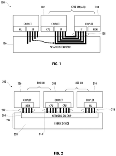
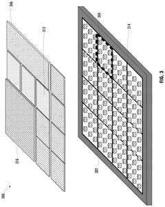
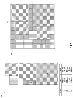
Modular chiplet system
PatentPendingUS20250029971A1
Innovation
- The modular chiplet system employs an active semiconductor substrate with a network-on-chip and a fabric device that includes a built-in network-on-chip, 3D chiplet interfaces, and a library of rotationally symmetrical chiplets. This system reduces lateral communication distances, enables efficient packet routing, and allows for the creation of various system permutations using a small set of chiplets and fabric devices.
Modular chip integration techniques
PatentActiveUS7741153B2
Innovation
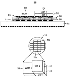
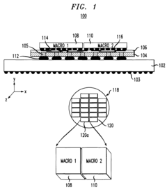
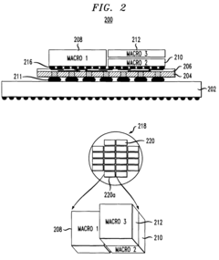
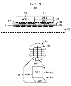
- The integration of chips and chip macros on a single carrier platform with segmented power and ground inputs and outputs to form voltage islands, using conductive vias and a wiring layer to facilitate the integration of heterogeneous chip technologies, allowing for the reuse of pre-designed components and supporting new chip designs with reduced power consumption.
Supply Chain Considerations for Chiplet Adoption
The adoption of chiplet technology across emerging markets necessitates a robust and resilient supply chain framework. Current chiplet supply chains face significant fragmentation challenges, with different components often sourced from geographically dispersed manufacturers. This fragmentation introduces logistical complexities, particularly in regions with developing infrastructure where transportation and storage capabilities may be limited.
Semiconductor manufacturing capacity represents a critical bottleneck in chiplet adoption. While established markets like North America, Europe, and East Asia maintain sophisticated fabrication facilities, emerging markets frequently lack access to advanced node manufacturing capabilities. This disparity creates dependency relationships that can impede local innovation and increase costs through import duties and international shipping expenses.
Standardization efforts across the chiplet ecosystem remain inconsistent, complicating integration processes for new market entrants. Organizations such as the Universal Chiplet Interconnect Express (UCIe) consortium are working to establish unified protocols, but adoption rates vary significantly across different regions and market segments. Emerging markets often face additional challenges implementing these standards due to limited technical expertise and testing infrastructure.
Material sourcing presents another dimension of supply chain vulnerability. Chiplets require specialized materials including high-purity silicon, rare earth elements, and advanced packaging substrates. Many emerging markets lack domestic access to these critical components, creating potential for supply disruptions during geopolitical tensions or natural disasters. Developing local sourcing alternatives represents a strategic priority for sustainable chiplet ecosystem growth.
Testing and quality assurance infrastructure constitutes a frequently overlooked aspect of chiplet supply chains. The disaggregated nature of chiplet-based systems demands sophisticated testing methodologies at multiple integration stages. Emerging markets typically possess limited access to advanced testing equipment, potentially compromising product reliability and performance consistency.
Intellectual property considerations significantly impact supply chain development for chiplet technologies. Patent landscapes around key chiplet innovations remain concentrated among established semiconductor companies, creating potential barriers for new entrants. Emerging markets must navigate complex licensing arrangements while developing indigenous innovation capabilities to ensure long-term competitiveness.
Workforce development represents perhaps the most fundamental supply chain consideration. Chiplet design, integration, and testing require specialized technical expertise that remains scarce in many emerging markets. Educational institutions and industry partnerships must prioritize semiconductor-specific training programs to address this critical skills gap and enable sustainable local chiplet ecosystem development.
Standardization Efforts in Chiplet Technology
The standardization of chiplet technology represents a critical foundation for the broader adoption and integration of chiplets across emerging markets. Industry consortia such as the Universal Chiplet Interconnect Express (UCIe) have emerged as pivotal forces in establishing common frameworks for chiplet-to-chiplet communication. UCIe's specifications, released in 2022, define both physical and protocol layers for die-to-die interconnects, enabling multi-vendor chiplet ecosystems to flourish through standardized interfaces.
Beyond UCIe, other significant standardization initiatives include JEDEC's development of chiplet-specific memory interfaces and the Open Compute Project's efforts to standardize chiplet integration in data center applications. These collaborative frameworks are essential for reducing integration complexity and ensuring interoperability between chiplets from different manufacturers.
The Chiplet Design Exchange (CDX) format represents another milestone in standardization efforts, providing a common language for chiplet design information exchange. This format facilitates seamless collaboration between chiplet providers and system integrators, streamlining the integration process and reducing time-to-market for chiplet-based products.
Standardization challenges persist, particularly in thermal management protocols and testing methodologies for multi-die packages. Industry leaders including Intel, AMD, TSMC, and Samsung are actively contributing to these standardization efforts, recognizing that common standards will accelerate market adoption and expand chiplet applications beyond high-performance computing into emerging markets.
The Advanced Packaging Collective, formed in 2023, focuses specifically on standardizing manufacturing processes for chiplet integration, addressing yield and reliability concerns that have historically limited chiplet adoption in cost-sensitive markets. Their work on standardized testing protocols has been particularly valuable for quality assurance in heterogeneous integration scenarios.
Regulatory bodies are increasingly acknowledging the importance of chiplet standardization, with organizations like NIST in the United States and ETSI in Europe developing certification frameworks for chiplet-based systems. These frameworks aim to ensure security, reliability, and performance consistency across chiplet implementations.
The evolution of these standards will significantly impact the trajectory of chiplet adoption in emerging applications such as edge AI, IoT devices, and automotive systems. As standardization matures, we anticipate accelerated innovation cycles and reduced barriers to entry for smaller players in the semiconductor ecosystem, democratizing access to advanced chiplet technology across diverse market segments.
Unlock deeper insights with Patsnap Eureka Quick Research — get a full tech report to explore trends and direct your research. Try now!
Generate Your Research Report Instantly with AI Agent
Supercharge your innovation with Patsnap Eureka AI Agent Platform!