Research on Standard Compliance in Chiplet Integration Practices
OCT 15, 20259 MIN READ
Generate Your Research Report Instantly with AI Agent
Patsnap Eureka helps you evaluate technical feasibility & market potential.
Chiplet Integration Standards Evolution and Objectives
The evolution of chiplet integration standards represents a paradigm shift in semiconductor design and manufacturing, moving from monolithic system-on-chip (SoC) approaches toward more modular, heterogeneous integration methodologies. This transition began in the early 2010s when traditional Moore's Law scaling faced increasing technical and economic challenges. The initial standardization efforts emerged around 2016-2017, primarily led by industry consortia seeking to address interoperability issues in multi-die packaging.
The development trajectory has been characterized by three distinct phases. The first phase (2016-2018) focused on establishing physical interconnect specifications, with initiatives like TSMC's Chip-on-Wafer-on-Substrate (CoWoS) and Intel's Embedded Multi-die Interconnect Bridge (EMIB). These proprietary solutions demonstrated the viability of chiplet approaches but highlighted the need for industry-wide standards.
The second phase (2019-2021) saw the formation of key standardization bodies, including the Open Compute Project's Open Domain-Specific Architecture (OCP ODSA) and DARPA's Common Heterogeneous Integration and IP Reuse Strategies (CHIPS) program. During this period, the Universal Chiplet Interconnect Express (UCIe) consortium began taking shape, bringing together major semiconductor manufacturers, foundries, and system companies.
The current phase (2022-present) is marked by the formal release of comprehensive standards such as UCIe 1.0 in March 2022, which defines both the physical and protocol layers for die-to-die interconnection. Simultaneously, complementary standards like Compute Express Link (CXL) have evolved to address higher-level communication protocols that complement chiplet integration.
The primary objectives of chiplet integration standardization are multifaceted. Technical objectives include establishing interoperability between chiplets from different vendors, defining consistent electrical and physical interfaces, and ensuring signal integrity across die boundaries. Performance objectives focus on minimizing latency and maximizing bandwidth in die-to-die communications while optimizing power efficiency.
Economic objectives are equally important, aiming to create an open ecosystem that fosters competition and innovation while reducing development costs through IP reuse. This includes establishing a "chiplet marketplace" where pre-validated components can be integrated into complex systems with minimal additional engineering.
Looking forward, standardization efforts are increasingly focused on expanding beyond physical interconnects to include protocol standardization, thermal management specifications, and testing methodologies. The ultimate goal is to enable a "plug-and-play" approach to semiconductor design where chiplets from various vendors can be seamlessly integrated, dramatically reducing time-to-market for complex systems while enabling customization and optimization for specific applications.
Market Demand Analysis for Standardized Chiplet Solutions
The global chiplet market is experiencing unprecedented growth, driven by the increasing demand for high-performance computing solutions across various industries. Market research indicates that the chiplet technology market is projected to grow at a compound annual growth rate of 40% from 2023 to 2030, reaching significant market valuation by the end of the forecast period. This remarkable growth trajectory is primarily fueled by the semiconductor industry's shift away from traditional monolithic designs toward more modular and flexible chiplet-based architectures.
The demand for standardized chiplet solutions is particularly strong in data centers and cloud computing environments, where performance, power efficiency, and scalability are critical factors. Enterprise customers are increasingly seeking heterogeneous computing solutions that can efficiently handle diverse workloads, including artificial intelligence, machine learning, and big data analytics. These applications require specialized processing capabilities that can be more effectively delivered through standardized chiplet integration.
Consumer electronics manufacturers represent another significant market segment driving demand for standardized chiplet solutions. As devices become more sophisticated and feature-rich, manufacturers are looking for ways to incorporate advanced computing capabilities while managing power consumption and form factor constraints. Standardized chiplet solutions offer a pathway to achieve these objectives by enabling the integration of specialized processing elements within compact device designs.
The automotive industry is emerging as a rapidly growing market for chiplet technology, particularly with the advancement of autonomous driving systems and in-vehicle infotainment. These applications demand high-performance computing capabilities with stringent reliability requirements, making standardized chiplet solutions an attractive option for automotive system designers.
Market analysis reveals a strong correlation between the adoption of standardized chiplet solutions and reduced time-to-market for new products. Companies implementing chiplet-based designs report development cycle reductions of up to 30% compared to traditional monolithic approaches. This acceleration in product development represents a significant competitive advantage in fast-moving technology markets.
From a geographical perspective, North America currently leads in chiplet technology adoption, followed closely by Asia-Pacific, particularly Taiwan, South Korea, and China. Europe is showing increasing interest, especially in automotive and industrial applications. The market demand is further strengthened by government initiatives worldwide that aim to bolster domestic semiconductor capabilities, with chiplet technology often highlighted as a strategic focus area for investment and development.
Current Compliance Challenges in Chiplet Integration
The integration of chiplets presents significant compliance challenges that must be addressed to ensure successful implementation. Current standards for chiplet integration remain fragmented across different industry bodies, creating confusion for manufacturers attempting to develop compliant solutions. The UCIe (Universal Chiplet Interconnect Express) consortium has established promising standards for die-to-die interconnects, but many companies struggle with interpreting and implementing these specifications correctly, particularly regarding signal integrity requirements and power delivery specifications.
Physical integration compliance issues are especially prominent, with thermal management standards varying widely across different application domains. The lack of unified thermal design power (TDP) guidelines for heterogeneous integration leads to inconsistent approaches in managing heat dissipation across chiplet interfaces. Additionally, mechanical stress tolerances and coefficient of thermal expansion (CTE) mismatch parameters remain inadequately standardized, resulting in reliability concerns for multi-vendor chiplet solutions.
Testing and verification present another major compliance challenge. Current test methodologies developed for monolithic chips are often inadequate for chiplet-based designs, where interconnect testing becomes significantly more complex. The industry lacks standardized test protocols for evaluating die-to-die interfaces at both the physical and protocol levels. Known good die (KGD) certification processes also vary substantially between manufacturers, complicating supply chain integration and quality assurance.
Intellectual property (IP) protection and security compliance introduce additional layers of complexity. The multi-vendor nature of chiplet ecosystems creates uncertainty regarding security boundaries and responsibility allocation for potential vulnerabilities. Current security standards inadequately address the unique challenges of protecting data as it traverses between chiplets from different vendors, with inconsistent implementation of encryption and authentication protocols at die-to-die interfaces.
Interoperability remains perhaps the most pressing compliance challenge. Despite efforts from organizations like JEDEC and OCP, the industry still lacks comprehensive interoperability frameworks that ensure chiplets from different vendors can seamlessly work together. Protocol compatibility issues frequently arise when integrating chiplets with different interface specifications, and the absence of standardized middleware solutions complicates system-level integration.
Regulatory compliance adds further complexity, with different regions implementing varying requirements for electronic components. Chiplet manufacturers must navigate these disparate regulations while ensuring their products remain globally marketable. The lack of harmonized international standards specifically addressing chiplet technology creates uncertainty regarding certification processes and compliance documentation requirements.
Current Compliance Frameworks and Implementation Methods
01 Universal Chiplet Interconnect Express (UCIe) Standards
Universal Chiplet Interconnect Express (UCIe) is a key standard for chiplet integration that defines protocols, physical interfaces, and power management for die-to-die interconnects. It enables interoperability between chiplets from different vendors, supporting high-bandwidth, low-latency communication while ensuring compliance with industry specifications for reliable integration in heterogeneous systems.- Universal Chiplet Interconnect Express (UCIe) Standard Compliance: The Universal Chiplet Interconnect Express (UCIe) standard provides specifications for die-to-die interconnects in multi-chiplet packages. Compliance with UCIe ensures interoperability between chiplets from different vendors, standardizing physical layer, protocol layer, and software stack interfaces. This enables a modular approach to semiconductor design where chiplets can be mixed and matched while maintaining reliable communication pathways and performance metrics.
- Advanced Interface Bus (AIB) Standard Implementation: The Advanced Interface Bus (AIB) standard provides specifications for chiplet-to-chiplet interconnects in heterogeneous integration. Implementing AIB standards ensures reliable high-bandwidth, low-latency communication between chiplets while maintaining power efficiency. The standard defines electrical specifications, physical layer protocols, and testing methodologies to verify compliance, enabling interoperability between chiplets from different manufacturers in a single package.
- Compliance Testing and Verification Methodologies: Specialized testing methodologies are essential for verifying chiplet integration standard compliance. These include automated test equipment configurations, built-in self-test circuits, and protocol analyzers designed specifically for chiplet interfaces. Verification processes validate signal integrity, timing parameters, power consumption, and protocol adherence across different operating conditions. Comprehensive compliance testing ensures reliable operation when integrating chiplets from multiple vendors in a single package.
- Thermal and Power Management Standard Compliance: Thermal and power management standards for chiplet integration address the unique challenges of heterogeneous integration. These standards define specifications for thermal interface materials, power delivery networks, and thermal dissipation pathways optimized for multi-die packages. Compliance ensures consistent performance across operating conditions, prevents thermal hotspots, and enables dynamic power management across chiplet boundaries, which is critical for system reliability and energy efficiency.
- Packaging and Assembly Standards for Chiplet Integration: Packaging and assembly standards for chiplet integration define requirements for substrate design, die attachment, interconnect formation, and encapsulation processes. These standards ensure mechanical stability, electrical performance, and reliability of multi-chiplet packages. Compliance with these standards facilitates manufacturing scalability and yield improvement through standardized processes, materials, and quality control methodologies, while enabling interoperability between chiplets from different vendors.
02 Testing and Verification for Standard Compliance
Testing and verification methodologies are essential for ensuring chiplet integration standard compliance. These include automated test frameworks, compliance verification tools, and validation procedures that check signal integrity, timing parameters, and protocol adherence. Such testing ensures chiplets meet specified standards before integration, reducing compatibility issues and improving overall system reliability.Expand Specific Solutions03 Advanced Packaging Technologies for Standard-Compliant Integration
Advanced packaging technologies support standard-compliant chiplet integration through specialized interconnect structures, substrate designs, and thermal management solutions. These technologies include silicon interposers, organic substrates with embedded bridges, and fan-out wafer-level packaging that accommodate standardized interfaces while optimizing signal integrity, power delivery, and thermal performance for heterogeneous integration.Expand Specific Solutions04 Interoperability Frameworks for Multi-Vendor Chiplets
Interoperability frameworks enable seamless integration of chiplets from different vendors by implementing standardized interfaces, communication protocols, and power management schemes. These frameworks include middleware solutions, abstraction layers, and reference designs that ensure chiplets can work together regardless of their origin, while maintaining compliance with industry standards for reliable system-level integration.Expand Specific Solutions05 Design Automation Tools for Standard-Compliant Chiplet Design
Design automation tools facilitate standard-compliant chiplet design through specialized software for interface generation, verification, and optimization. These tools include electronic design automation (EDA) platforms with built-in standard compliance checking, interface generators that automatically create standard-compliant interconnects, and design-for-test features that ensure manufactured chiplets will meet required specifications for successful integration.Expand Specific Solutions
Key Industry Players in Chiplet Standards Development
The chiplet integration standards landscape is evolving rapidly, with the market currently in a growth phase characterized by increasing adoption across high-performance computing applications. Major semiconductor players including TSMC, Intel, AMD (formerly ATI), and NVIDIA are driving standardization efforts, with each developing proprietary and open approaches to chiplet interconnection. The technology is approaching early maturity in specific applications, though full industry-wide standardization remains in development. Companies like Huawei, Qualcomm, and Micron are investing heavily in compliance frameworks, while academic institutions such as Nanjing University of Posts & Telecommunications collaborate with industry to establish testing methodologies. The market is projected to exceed $50 billion by 2030, driven by data center, AI, and high-performance computing demands requiring modular chip designs with standardized interfaces.
Taiwan Semiconductor Manufacturing Co., Ltd.
Technical Solution: TSMC has developed comprehensive standard compliance frameworks for chiplet integration through its advanced packaging technologies, including Chip-on-Wafer-on-Substrate (CoWoS), Integrated Fan-Out (InFO), and System-on-Integrated-Chips (SoIC). TSMC's 3DFabric platform represents a unified approach to chiplet integration that adheres to industry standards while providing manufacturing scalability. Their compliance strategy focuses on standardizing die-to-die (D2D) interfaces and ensuring signal integrity across heterogeneous integration processes. TSMC has implemented rigorous testing protocols for thermal management, power delivery, and mechanical stress that exceed industry requirements. They actively participate in the UCIe consortium and have developed proprietary verification methodologies to ensure chiplets from different vendors can be integrated seamlessly[2]. TSMC's approach includes standardized design kits that help clients implement chiplet designs that comply with both electrical and physical interface specifications, facilitating multi-vendor chiplet ecosystems.
Strengths: As the world's largest foundry, TSMC's standards often become de facto industry norms. Their advanced packaging technologies provide practical implementation paths for theoretical standards. Weaknesses: Their proprietary nature of some integration technologies may limit broader ecosystem adoption. High costs associated with advanced packaging technologies may restrict accessibility to smaller players.
NVIDIA Corp.
Technical Solution: NVIDIA has developed a comprehensive approach to chiplet integration standard compliance through its NVLink interconnect technology and multi-chip-module (MCM) designs. Their Grace Hopper Superchip exemplifies standard-compliant chiplet integration, combining an Arm-based CPU with a Hopper GPU using NVIDIA's chip-to-chip interconnect that delivers 900 GB/s bandwidth with 5x the energy efficiency of PCIe Gen5[4]. NVIDIA's compliance strategy focuses on standardizing high-bandwidth, low-latency interconnects between heterogeneous chiplets while maintaining software compatibility. Their NVSwitch fabric technology enables standardized communication between multiple chiplets in high-performance computing environments. NVIDIA has also pioneered standardized testing methodologies for thermal and power management across chiplet boundaries, ensuring reliable operation under extreme computational loads. Their participation in the UCIe consortium demonstrates commitment to open standards while maintaining proprietary advantages in GPU-accelerated computing architectures.
Strengths: NVIDIA's interconnect technologies offer industry-leading bandwidth and energy efficiency. Their software ecosystem provides standardized programming models across heterogeneous chiplet architectures. Weaknesses: Heavy focus on GPU-centric architectures may limit applicability in some domains. Proprietary nature of some technologies may create vendor lock-in despite standards participation.
Critical Patents and Technical Literature in Chiplet Standards
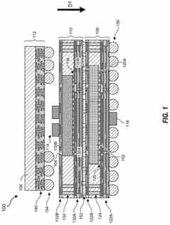
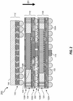
3D chiplet integration using fan-out wafer-level packaging
PatentPendingUS20240274587A1
Innovation
- The use of fan-out wafer-level packaging and three-dimensional packaging techniques for combining semiconductor chips and embedded memory in configurations such as face-to-back, back-to-back, and face-to-face orientations, enabling direct connections between chiplets and reducing assembly package sizes and manufacturing complexity.
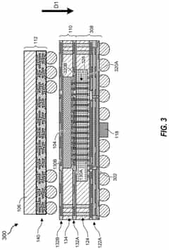
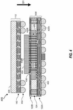
Integrated structure and integration method suitable for wafer-scale heterogeneous chiplet
PatentWO2024011880A1
Innovation
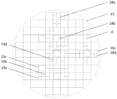
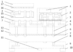
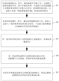
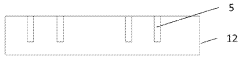
- By setting a through silicon via array and repeated standard integration areas on the wafer substrate, and preparing a silicon transfer board with heterogeneous transfer board micro-bumps and micro-pads, a standard integrated part is formed to realize heterogeneous cores. The die is bonded to the wafer substrate, and multi-layer rewiring layers are used to realize the interconnection between the die.
Interoperability Testing Methodologies for Chiplet Integration
Interoperability testing for chiplet integration represents a critical component in ensuring that diverse chiplet components from multiple vendors can function cohesively within a single package. The methodology for such testing must be comprehensive, addressing both physical and logical interfaces between chiplets, as well as performance characteristics under various operating conditions.
Standard compliance testing methodologies typically begin with interface validation, where electrical parameters such as signal integrity, timing margins, and power delivery are rigorously measured against established specifications like UCIe (Universal Chiplet Interconnect Express), AIB (Advanced Interface Bus), or BoW (Bunch of Wires). These tests utilize specialized equipment including high-speed oscilloscopes, vector network analyzers, and automated test equipment (ATE) platforms configured for chiplet-specific testing scenarios.
Protocol-level testing forms the second layer of interoperability assessment, focusing on the communication protocols between chiplets. This involves verification of handshaking procedures, data packet formation and transmission, error detection and correction mechanisms, and flow control capabilities. Protocol analyzers and FPGA-based test platforms are commonly employed to simulate various traffic patterns and stress conditions.
System-level interoperability testing examines how chiplets function collectively within the complete package. This includes thermal management testing under various workloads, power state transitions, and system recovery from fault conditions. Advanced thermal imaging equipment and power analyzers are utilized to monitor system behavior during these tests.
Regression testing methodologies ensure that chiplet integration remains robust across firmware updates and design iterations. Automated test suites that can be repeatedly executed provide consistency in verification across product development cycles and help identify any regressions in functionality or performance.
Compliance certification processes typically involve third-party validation laboratories that can independently verify adherence to industry standards. These laboratories maintain reference implementations and "golden" test vectors that serve as benchmarks for chiplet interoperability. The certification process often includes documentation review, physical testing, and interoperability demonstrations with reference designs.
Cross-vendor validation represents perhaps the most challenging aspect of chiplet interoperability testing. This requires coordinated test plans between multiple semiconductor companies, often facilitated through industry consortia or standards bodies. Plug-fests and interoperability workshops provide venues for vendors to test their chiplets against implementations from other manufacturers in controlled environments.
Regulatory Implications for Chiplet-Based System Design
The regulatory landscape for chiplet-based system design is becoming increasingly complex as this technology gains prominence in the semiconductor industry. Compliance with international standards such as IEEE 2401 (Standard for Design and Verification of Chiplet Interconnects) and JEDEC JEP30 (Guidelines for Chiplet Integration) is now essential for manufacturers seeking global market access. These standards establish baseline requirements for signal integrity, power management, and thermal performance that directly impact system reliability and certification processes.
Regulatory bodies across different regions have begun implementing specific requirements for chiplet-based systems. In the United States, the Federal Communications Commission (FCC) has updated its electromagnetic compatibility (EMC) testing protocols to address the unique interference patterns that can emerge from multi-die packages. Similarly, the European Union's CE marking process now includes additional verification steps for chiplet-based products, particularly focusing on power efficiency metrics under the Ecodesign Directive.
Security and data protection regulations present another significant compliance challenge. The heterogeneous nature of chiplet designs, often incorporating components from multiple vendors, creates potential security vulnerabilities that must be addressed to meet regulations such as the EU's Cyber Resilience Act and the U.S. Executive Order on Improving the Nation's Cybersecurity. Manufacturers must implement robust security measures at the die-to-die interfaces and demonstrate compliance through comprehensive documentation.
Supply chain regulations are evolving to address the distributed manufacturing model common in chiplet production. The CHIPS Act in the United States and similar initiatives in Europe and Asia have introduced new reporting requirements regarding component sourcing and manufacturing processes. Companies must maintain detailed records of chiplet origins and integration methods to satisfy these regulations, particularly for applications in critical infrastructure or defense systems.
Environmental regulations are also impacting chiplet design practices. RoHS and WEEE directives in Europe, along with similar regulations worldwide, require careful material selection and end-of-life planning. The modular nature of chiplet designs offers potential advantages for recyclability and component reuse, but manufacturers must document compliance with substance restrictions and develop appropriate disposal protocols.
Looking forward, regulatory frameworks are likely to evolve toward performance-based standards rather than prescriptive requirements, allowing greater flexibility in chiplet implementation while maintaining necessary safeguards. Industry consortia such as the Universal Chiplet Interconnect Express (UCIe) are working with regulatory bodies to develop standardized compliance testing methodologies that can streamline certification processes while ensuring system safety and reliability.
Unlock deeper insights with Patsnap Eureka Quick Research — get a full tech report to explore trends and direct your research. Try now!
Generate Your Research Report Instantly with AI Agent
Supercharge your innovation with Patsnap Eureka AI Agent Platform!