

What Factors Influence Chiplet Integration in Electronics Design
OCT 15, 20259 MIN READ
Generate Your Research Report Instantly with AI Agent
Patsnap Eureka helps you evaluate technical feasibility & market potential.
Chiplet Integration Background and Objectives
Chiplet integration represents a paradigm shift in semiconductor design and manufacturing, emerging as a response to the slowing of Moore's Law and the increasing challenges in traditional monolithic chip scaling. This approach involves disaggregating complex system-on-chip (SoC) designs into smaller functional blocks called chiplets, which are then integrated using advanced packaging technologies. The evolution of chiplet technology can be traced back to the early 2010s, with significant acceleration in development over the past five years as semiconductor manufacturers sought alternatives to traditional scaling methods.
The technological trajectory of chiplet integration has been shaped by several key factors, including the physical limitations of silicon scaling, increasing design complexity, and rising manufacturing costs for advanced process nodes. As transistor dimensions approach atomic scales, the benefits of traditional node shrinking have diminished while costs have escalated exponentially. Chiplet architecture offers a compelling alternative by allowing different components to be manufactured using optimal process technologies and then combined into a single package.
Industry momentum behind chiplet integration has grown substantially, with major semiconductor companies including Intel, AMD, TSMC, and Samsung all investing heavily in this approach. The formation of industry consortia such as the Universal Chiplet Interconnect Express (UCIe) in 2022 marked a significant milestone in establishing standards for chiplet-to-chiplet communication, signaling the industry's commitment to this architectural paradigm.
The primary technical objectives of chiplet integration include achieving performance comparable to monolithic designs while offering greater flexibility, improved yield, and potentially lower costs. Specific goals encompass developing high-bandwidth, low-latency die-to-die interconnects; establishing standardized interfaces for interoperability; creating efficient thermal management solutions for multi-die packages; and developing advanced packaging technologies that can accommodate increasingly complex chiplet arrangements.
Looking forward, chiplet integration aims to enable more specialized and heterogeneous computing architectures, where different types of processing elements (CPUs, GPUs, AI accelerators, etc.) can be optimally combined within a single package. This approach is particularly relevant for emerging applications in artificial intelligence, high-performance computing, and edge computing, where specialized processing capabilities and energy efficiency are paramount.
The ultimate vision for chiplet technology extends beyond current implementations toward a "plug-and-play" ecosystem where chiplets from different vendors can be seamlessly integrated, potentially revolutionizing the semiconductor industry's business models and supply chains while enabling unprecedented levels of customization and optimization for specific applications.
Market Demand Analysis for Chiplet Technology
The global chiplet market is experiencing unprecedented growth, driven by the increasing demand for high-performance computing solutions across various industries. Current market projections indicate that the chiplet technology market is expected to grow at a compound annual growth rate of over 40% from 2023 to 2030, potentially reaching a market value of tens of billions of dollars by the end of the decade. This remarkable growth trajectory is primarily fueled by the semiconductor industry's shift away from traditional monolithic designs toward more modular and efficient chiplet-based architectures.
The demand for chiplet technology is particularly strong in data centers and cloud computing environments, where the need for processing power continues to escalate due to artificial intelligence, machine learning, and big data applications. These computational workloads require increasingly powerful processors that traditional monolithic designs struggle to deliver cost-effectively. Chiplet-based solutions offer a compelling alternative by enabling higher performance, improved power efficiency, and better yield management.
Consumer electronics represents another significant market segment driving chiplet adoption. As smartphones, tablets, and other personal devices incorporate more advanced features such as AI processing, augmented reality, and computational photography, the demand for more powerful yet energy-efficient processors grows. Chiplet technology allows device manufacturers to customize their silicon solutions while maintaining competitive pricing and performance characteristics.
The automotive industry is emerging as a rapidly growing market for chiplet technology, particularly with the advancement of autonomous driving systems and electric vehicles. These applications require sophisticated computing platforms that can process vast amounts of sensor data in real-time while operating within strict power and thermal constraints. Chiplet-based designs offer the flexibility and performance needed for these demanding automotive applications.
Telecommunications infrastructure, particularly with the ongoing deployment of 5G networks and the future development of 6G, represents another significant market opportunity for chiplet technology. The need for high-bandwidth, low-latency communication systems drives demand for advanced processing capabilities that chiplets can efficiently deliver.
From a geographical perspective, North America and Asia-Pacific currently dominate the chiplet market, with major semiconductor companies and foundries investing heavily in chiplet research and manufacturing capabilities. Europe is also increasing its investments in chiplet technology as part of broader initiatives to strengthen its semiconductor ecosystem and reduce dependence on external suppliers.
The market demand for chiplet technology is further accelerated by industry-wide efforts to establish standards for chiplet interfaces and integration methodologies, which will facilitate broader adoption across different market segments and applications.
Current Challenges in Chiplet Integration
Despite the promising potential of chiplet technology, several significant challenges impede its widespread adoption and integration into mainstream electronics design. The foremost challenge lies in the standardization of interfaces between chiplets. Currently, the industry lacks universally accepted protocols and physical interfaces, resulting in compatibility issues when integrating chiplets from different manufacturers. This fragmentation creates significant barriers to the development of a robust chiplet ecosystem.
Thermal management presents another critical challenge in chiplet integration. As multiple dies are packed closely together, heat dissipation becomes increasingly complex. The thermal interface materials between chiplets and heat spreaders often create bottlenecks in heat transfer, potentially leading to performance degradation or reliability issues. Advanced cooling solutions specifically designed for chiplet architectures are still in early development stages.
Testing and validation methodologies for chiplet-based systems remain underdeveloped. Traditional testing approaches designed for monolithic chips are insufficient for multi-die configurations. Known-good-die testing becomes particularly challenging as chiplets may exhibit different behaviors when integrated into a system compared to when tested individually. This increases manufacturing complexity and potentially impacts yield rates.
The physical integration of chiplets introduces mechanical stress concerns. Different thermal expansion coefficients between materials can lead to warpage and connection failures over time. Additionally, the miniaturization of interconnects between chiplets increases susceptibility to electromigration and other reliability issues, particularly in high-performance applications.
Supply chain complexity represents a significant operational challenge. Chiplet-based designs often involve multiple vendors supplying different components, requiring sophisticated coordination and quality control processes. This multi-vendor approach introduces potential bottlenecks in production and complicates failure analysis when issues arise.
Economic factors also present obstacles to chiplet adoption. The initial investment required for chiplet design and manufacturing infrastructure is substantial. While chiplet approaches may reduce costs in high-volume production, the break-even point can be challenging to achieve for smaller production runs. Furthermore, intellectual property protection and licensing models for chiplet designs remain complex and potentially restrictive.
Design tools and methodologies specifically optimized for chiplet-based systems are still evolving. Current electronic design automation (EDA) tools often lack comprehensive support for multi-die optimization, particularly for power, thermal, and signal integrity analyses across chiplet boundaries. This gap in design infrastructure increases development time and engineering costs.
Current Chiplet Integration Methodologies
01 Interconnect technologies for chiplet integration
Various interconnect technologies are crucial for effective chiplet integration, enabling high-bandwidth, low-latency communication between different chiplets. These technologies include advanced packaging methods such as silicon interposers, organic substrates, and through-silicon vias (TSVs). The interconnect architecture significantly impacts the overall performance, power efficiency, and reliability of multi-chiplet systems, with different approaches optimized for specific applications and performance requirements.- Interconnect technologies for chiplet integration: Various interconnect technologies are crucial for effective chiplet integration, enabling high-bandwidth, low-latency communication between different chiplets. These technologies include advanced packaging methods such as silicon interposers, organic substrates, and through-silicon vias (TSVs). The interconnect architecture significantly impacts the overall performance, power efficiency, and thermal characteristics of multi-chiplet systems, with different approaches optimized for specific applications and performance requirements.
- Thermal management in chiplet designs: Thermal management is a critical integration factor in chiplet-based architectures. As multiple chiplets are integrated into a single package, heat dissipation becomes more complex and challenging. Advanced cooling solutions, thermal interface materials, and strategic placement of chiplets based on their thermal profiles are essential considerations. Effective thermal management techniques include the use of heat spreaders, integrated liquid cooling channels, and thermally-aware floorplanning to ensure optimal performance and reliability of the integrated system.
- Power delivery network optimization: Optimizing power delivery networks is essential for chiplet integration, as it ensures stable and efficient power distribution across multiple chiplets. This involves careful design of power planes, decoupling capacitors, and voltage regulators to minimize power noise and ensure voltage stability. Advanced power delivery techniques include integrated voltage regulators, point-of-load power conversion, and heterogeneous power domains tailored to the specific requirements of different chiplets, enabling improved energy efficiency and performance in complex multi-chiplet systems.
- Testing and yield management strategies: Testing and yield management are crucial factors in chiplet integration, affecting both manufacturing costs and product reliability. Known-good-die testing before integration, built-in self-test mechanisms, and post-integration validation methodologies are essential to ensure functionality. Advanced approaches include hierarchical testing strategies, partial reconfiguration capabilities to bypass defective components, and yield-aware chiplet placement. These strategies help maximize overall system yield and reliability while minimizing manufacturing costs in complex multi-chiplet architectures.
- Heterogeneous integration and process technology compatibility: Heterogeneous integration enables combining chiplets manufactured using different process technologies, allowing optimization of each component for its specific function. This approach presents challenges in managing different material properties, thermal expansion coefficients, and electrical characteristics. Solutions include advanced interface standards, die-to-die communication protocols, and adaptive compensation techniques. Successful heterogeneous integration enables combining high-performance logic, memory, analog, and RF components in a single package, offering significant advantages in performance, power efficiency, and system flexibility.
02 Thermal management considerations in chiplet designs
Thermal management is a critical factor in chiplet integration, as the dense packaging of multiple chiplets can lead to significant heat generation and potential hotspots. Advanced cooling solutions, including integrated heat spreaders, microchannel cooling, and thermal interface materials, are employed to maintain optimal operating temperatures. Effective thermal design must account for power density variations across different chiplets and ensure uniform heat dissipation to prevent thermal throttling and maintain system reliability.Expand Specific Solutions03 Power delivery network optimization for chiplet systems
Power delivery networks for chiplet-based systems require careful optimization to ensure stable voltage supply across multiple integrated components. This involves designing efficient power distribution architectures, implementing advanced voltage regulation techniques, and managing power domains across chiplet boundaries. Considerations include minimizing IR drop, reducing power noise, and implementing power-saving features while maintaining performance requirements for heterogeneous chiplet configurations.Expand Specific Solutions04 Testing and validation methodologies for multi-chiplet systems
Testing and validation of multi-chiplet systems present unique challenges compared to monolithic designs. Comprehensive methodologies include pre-integration testing of individual chiplets, interface validation between chiplets, and system-level functional testing. Advanced techniques such as built-in self-test (BIST), boundary scan testing, and known-good-die strategies are employed to ensure reliability and yield. Post-packaging testing is also critical to verify the integrity of interconnects and overall system functionality under various operating conditions.Expand Specific Solutions05 Design partitioning strategies for heterogeneous integration
Effective design partitioning is fundamental to successful chiplet integration, particularly for heterogeneous systems combining different process technologies or functional blocks. This involves determining optimal boundaries between chiplets based on factors such as communication bandwidth requirements, manufacturing considerations, and yield optimization. Strategic partitioning decisions must balance performance objectives with practical constraints related to die size, I/O density, and system architecture, while enabling independent optimization of different functional components.Expand Specific Solutions
Key Industry Players in Chiplet Ecosystem
Chiplet integration in electronics design is evolving rapidly, currently transitioning from early adoption to mainstream implementation. The market is experiencing significant growth, projected to reach billions by 2025, driven by demands for higher performance and cost efficiency. Technology maturity varies across players: Intel, AMD, and TSMC lead with advanced packaging technologies like EMIB, Infinity Fabric, and CoWoS; Qualcomm and IBM are advancing heterogeneous integration; while newer entrants like Huawei and Moore Thread are developing competitive solutions. Universities including Xidian and Fudan contribute fundamental research. The ecosystem is expanding as semiconductor manufacturers recognize chiplets as essential for overcoming monolithic design limitations and enabling specialized functionality integration.
Intel Corp.
Technical Solution: Intel has pioneered chiplet integration through its EMIB (Embedded Multi-die Interconnect Bridge) and Foveros 3D packaging technologies. EMIB uses silicon bridges embedded in the package substrate to connect chiplets horizontally with high-bandwidth, short-reach connections. This approach eliminates the need for silicon interposers while maintaining high connection density. Intel's Foveros technology enables true 3D stacking of logic chips, allowing for vertical integration of heterogeneous chiplets. Intel has implemented these technologies in products like Lakefield processors and Ponte Vecchio GPUs, demonstrating up to 2x improvement in interconnect density compared to traditional 2.5D approaches. Intel's Advanced Interface Bus (AIB) protocol facilitates chiplet communication with reported bandwidths of 2 Gbps/pin while consuming 0.85pJ/bit, enabling modular chip design across different process nodes.
Strengths: Mature packaging technologies with proven products in market; comprehensive ecosystem including design tools and manufacturing capabilities; strong IP portfolio in chiplet interconnects. Weaknesses: Higher implementation costs compared to monolithic designs; thermal management challenges in 3D stacked configurations; proprietary interconnect standards may limit industry-wide adoption.
QUALCOMM, Inc.
Technical Solution: Qualcomm has developed advanced chiplet integration strategies focusing on mobile and edge computing applications. Their approach leverages System-in-Package (SiP) technology that combines multiple chiplets in a single package to optimize performance, power efficiency, and form factor. Qualcomm's chiplet architecture employs high-density interconnects with reported bandwidths exceeding 1 Tbps between dies while maintaining power efficiency below 1 pJ/bit. Their RF-SOI (Radio Frequency Silicon-on-Insulator) technology enables integration of RF components with digital processing chiplets, critical for 5G applications. Qualcomm has implemented heterogeneous integration in their Snapdragon platforms, combining application processors, modems, and specialized accelerators as separate chiplets. Their approach emphasizes die-to-die interfaces that minimize latency (under 2ns) and power overhead while maximizing bandwidth for mobile applications where power constraints are paramount.
Strengths: Expertise in low-power chiplet designs optimized for mobile applications; strong integration capabilities for RF and mixed-signal components; established manufacturing partnerships for advanced packaging. Weaknesses: Solutions primarily optimized for mobile ecosystem rather than broader computing markets; reliance on external foundry partners for advanced manufacturing processes; thermal constraints in compact mobile form factors.
Critical Patents and Technical Innovations
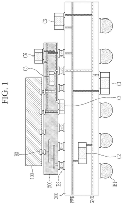
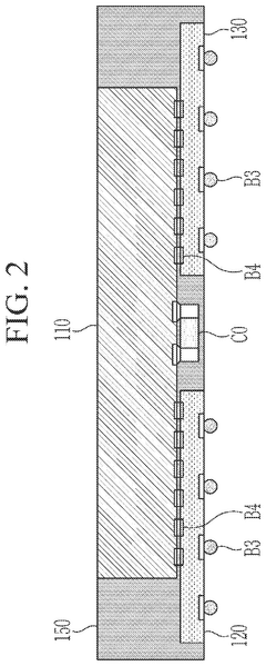
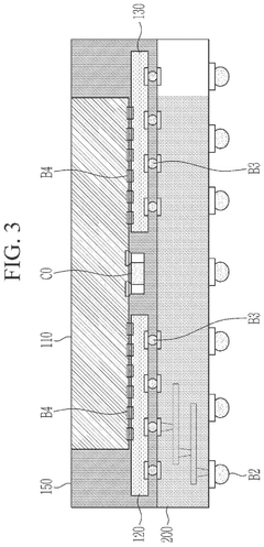
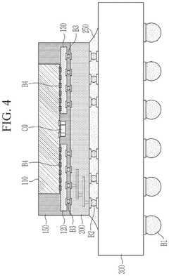
Semiconductor package with decoupling capacitor and method for manufacturing the same
PatentPendingUS20240332270A1
Innovation
- The implementation of chiplet technology to divide the semiconductor die into multiple dies, allowing for the placement of decoupling capacitors between these dies, ensuring they are closer to the active elements without reducing the number of input/output paths, and using hybrid bonding or solder bumps for connections.
Integrated circuit device including a multi-chip package
PatentPendingUS20250293204A1
Innovation
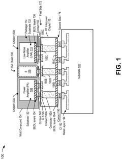
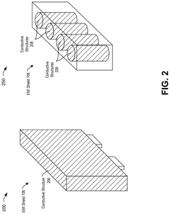
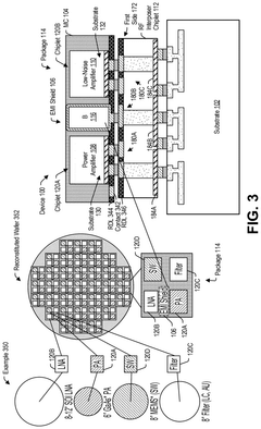
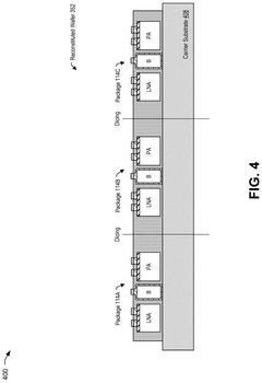
- A multi-chip package design incorporating a first chiplet with power amplifier circuitry, a second chiplet with low-noise amplifier circuitry, and an electromagnetic interference (EMI) shield between them, along with a radio frequency interposer chiplet, all encapsulated in a mold compound, to facilitate efficient electrical connections and reduce electromagnetic interference.
Standardization Efforts in Chiplet Interfaces
The standardization of chiplet interfaces represents a critical foundation for the broader adoption of chiplet technology across the semiconductor industry. Currently, several major standardization initiatives are driving the development of common interfaces that enable interoperability between chiplets from different vendors.
The Universal Chiplet Interconnect Express (UCIe) consortium, formed in 2022, has emerged as a leading force in chiplet interface standardization. Backed by industry giants including Intel, AMD, Arm, TSMC, and Samsung, UCIe aims to establish an open ecosystem for die-to-die interconnection. The standard defines both the physical layer and protocol stack for chiplet communication, supporting both package substrate and silicon interposer implementations.
Complementing UCIe, the Open Compute Project's Bunch of Wires (BoW) interface provides a simpler, lower-cost alternative focused on package substrate implementations. BoW offers scalable bandwidth from 16 Gbps to 112 Gbps per mm of die edge, making it suitable for a wide range of applications from cost-sensitive to high-performance computing.
Advanced Interface Bus (AIB) by Intel represents another significant standardization effort. Now in its third generation, AIB has been contributed to the CHIPS Alliance for broader industry adoption. It provides a die-to-die PHY-level interface specification that enables high-bandwidth, low-power connectivity between chiplets.
The High Bandwidth Memory (HBM) interface standard, while primarily focused on memory integration, has established important precedents for chiplet-based designs. Its through-silicon via (TSV) approach has influenced broader chiplet integration methodologies.
These standardization efforts face several challenges, including balancing performance requirements with implementation complexity, ensuring backward compatibility while enabling innovation, and addressing intellectual property concerns across competitive companies.
The economic implications of interface standardization are substantial. McKinsey research indicates that standardized interfaces could reduce chiplet integration costs by 25-40% and accelerate time-to-market by up to 30%. This cost reduction is critical for making chiplet technology economically viable across more market segments.
Looking forward, emerging standards are beginning to address not just electrical interfaces but also thermal management, mechanical specifications, and testing methodologies for chiplets. The JEDEC JC-70 committee is developing standards for known-good-die testing and handling, which will further facilitate chiplet adoption across the industry.
Thermal Management Considerations for Chiplet Systems
Thermal management has emerged as a critical factor in chiplet integration, directly impacting system performance, reliability, and longevity. As chiplet architectures pack more computing power into smaller spaces, heat dissipation challenges intensify significantly. The thermal density of chiplet-based systems often exceeds that of monolithic designs due to the concentration of active components and the thermal resistance introduced at integration interfaces.
The heterogeneous nature of chiplet systems creates complex thermal profiles, with different chiplets potentially operating at varying power levels and temperature thresholds. This non-uniform heat distribution necessitates sophisticated thermal management strategies beyond traditional cooling methods. Thermal interface materials (TIMs) between chiplets and heat spreaders play a crucial role, with research showing that TIM performance can impact overall system temperature by 10-15°C under load conditions.
Interposer materials significantly influence thermal conductivity pathways. Silicon interposers offer thermal conductivity around 150 W/mK, while organic substrates typically provide only 0.3-0.5 W/mK. This substantial difference affects how heat distributes throughout the package and ultimately reaches cooling solutions. Advanced packaging technologies like embedded silicon bridges or through-silicon vias (TSVs) can be leveraged as thermal conduits, serving dual purposes for electrical connectivity and heat transfer.
Dynamic thermal management (DTM) techniques have become essential for chiplet systems, with adaptive algorithms that monitor temperature across different chiplets and adjust workloads or clock frequencies accordingly. These systems must respond to thermal emergencies within microseconds to prevent damage while maximizing performance during normal operation. Research indicates that effective DTM implementations can maintain performance within 5% of theoretical maximums while keeping temperatures below critical thresholds.
Cooling solution design for chiplet systems requires careful consideration of the entire thermal stack. Direct liquid cooling approaches are gaining traction, with targeted cooling of high-power chiplets showing 30-40% improved thermal performance compared to traditional air cooling. Computational fluid dynamics (CFD) modeling has become an indispensable tool in the design process, allowing engineers to predict hotspots and optimize cooling solutions before physical prototyping.
The industry is witnessing innovation in specialized cooling solutions for chiplet architectures, including microchannel liquid cooling integrated directly into interposers and vapor chambers designed to spread heat from concentrated sources. These technologies aim to address the fundamental thermal challenges of chiplet integration while enabling continued scaling of performance and functionality in next-generation electronic systems.
Unlock deeper insights with Patsnap Eureka Quick Research — get a full tech report to explore trends and direct your research. Try now!
Generate Your Research Report Instantly with AI Agent
Supercharge your innovation with Patsnap Eureka AI Agent Platform!