How Chiplet Integration Advances Market Standards in Technology
OCT 15, 20259 MIN READ
Generate Your Research Report Instantly with AI Agent
Patsnap Eureka helps you evaluate technical feasibility & market potential.
Chiplet Technology Evolution and Objectives
Chiplet technology represents a paradigm shift in semiconductor design and manufacturing, evolving from traditional monolithic integrated circuits to a more modular approach. This evolution began in the early 2010s when semiconductor manufacturers faced increasing challenges with Moore's Law, as the physical limitations of silicon-based transistor miniaturization became apparent. The industry's response was to decompose complex system-on-chip (SoC) designs into smaller, more manageable chiplets that could be manufactured separately and then integrated using advanced packaging technologies.
The evolution of chiplet technology has been marked by several key milestones. Initially, companies like AMD pioneered the commercial use of chiplets with their Zen architecture in 2017, demonstrating significant improvements in manufacturing yield and cost efficiency. Subsequently, Intel introduced its Embedded Multi-die Interconnect Bridge (EMIB) and Foveros technologies, while TSMC developed its Integrated Fan-Out (InFO) and System on Integrated Chips (SoIC) solutions, all aimed at enhancing chiplet integration capabilities.
The primary objective of chiplet technology is to overcome the economic and technical barriers associated with monolithic chip designs. As process nodes shrink below 7nm, the cost and complexity of manufacturing large, monolithic chips increase exponentially. Chiplets allow manufacturers to optimize different components of a system using the most appropriate process node for each function, thereby maximizing performance while minimizing costs.
Another critical objective is to enable greater design flexibility and reusability. By standardizing chiplet interfaces and packaging technologies, semiconductor companies can mix and match pre-designed chiplets from different vendors, accelerating time-to-market and reducing development costs. This modular approach also facilitates more efficient product updates, as individual chiplets can be upgraded without redesigning the entire system.
Looking forward, the chiplet ecosystem aims to establish industry-wide standards for chiplet interfaces, packaging, and testing methodologies. Organizations like the Universal Chiplet Interconnect Express (UCIe) consortium are working to create open specifications that will enable interoperability between chiplets from different manufacturers. The ultimate goal is to foster a more collaborative semiconductor industry where specialized chiplets can be sourced from various vendors and seamlessly integrated into high-performance computing systems.
The evolution of chiplet technology also aligns with broader industry trends toward heterogeneous computing and specialized accelerators. As artificial intelligence, high-performance computing, and edge computing continue to drive demand for more powerful and energy-efficient systems, chiplets offer a pathway to combine diverse computing architectures (CPUs, GPUs, FPGAs, ASICs) within a single package, optimized for specific workloads.
Market Demand Analysis for Chiplet Solutions
The global chiplet market is experiencing unprecedented growth, driven by the increasing demand for high-performance computing solutions across multiple industries. Current market projections indicate that the chiplet market will reach approximately $5.8 billion by 2024, with a compound annual growth rate (CAGR) of 40.9% from 2022 to 2027. This remarkable growth trajectory reflects the industry's recognition of chiplets as a viable solution to the limitations of traditional monolithic chip designs.
The primary market demand for chiplet solutions stems from data centers and cloud service providers seeking to optimize computational efficiency while managing power consumption. These sectors require increasingly powerful processors to handle complex workloads such as artificial intelligence, machine learning, and big data analytics. Traditional monolithic designs have reached physical limitations in terms of manufacturing yield and performance scaling, creating a significant market gap that chiplet technology effectively addresses.
Consumer electronics represents another substantial market segment driving chiplet adoption. Smartphone manufacturers, gaming console producers, and personal computing companies are all exploring chiplet integration to deliver enhanced performance within constrained form factors and thermal envelopes. Market research indicates that approximately 35% of high-end consumer electronics will incorporate some form of chiplet technology by 2025.
The automotive industry is emerging as a rapidly growing market for chiplet solutions, particularly with the advancement of autonomous driving technologies and in-vehicle infotainment systems. The need for high-performance, energy-efficient computing in vehicles has created a demand for specialized chiplet designs that can withstand harsh environmental conditions while delivering reliable performance.
Telecommunications infrastructure, particularly with the ongoing global 5G rollout and future 6G development, represents another significant market opportunity. Network equipment providers require increasingly sophisticated processing capabilities to handle the massive data throughput and low-latency requirements of modern communication networks.
Market analysis reveals regional variations in chiplet demand, with North America and Asia-Pacific leading adoption rates. North America dominates in terms of research and development investment, while Asia-Pacific leads in manufacturing capacity and implementation. Europe shows growing interest, particularly in automotive and industrial applications of chiplet technology.
The market is also witnessing increased demand for standardization across chiplet interfaces and integration methodologies. Industry consortia such as the Universal Chiplet Interconnect Express (UCIe) are gaining significant traction, with membership growing by 78% in 2022 alone, highlighting the industry's recognition that standardization is crucial for broader market adoption and ecosystem development.
Current Chiplet Integration Challenges
Despite the promising advancements in chiplet technology, significant technical challenges persist that impede widespread adoption and standardization. Integration complexity represents the foremost obstacle, as connecting multiple chiplets requires sophisticated packaging technologies and precise alignment mechanisms. The current approaches—including silicon interposers, organic substrates, and advanced bridge technologies—each present unique manufacturing difficulties and yield concerns when implemented at scale.
Thermal management emerges as another critical challenge, particularly as chiplet designs become more complex. The concentration of multiple dies in close proximity creates thermal hotspots that can compromise performance and reliability. Existing cooling solutions designed for monolithic chips often prove inadequate for the three-dimensional thermal profiles of chiplet architectures.
Interconnect bandwidth limitations continue to constrain chiplet integration potential. While technologies like EMIB (Embedded Multi-die Interconnect Bridge) and CoWoS (Chip-on-Wafer-on-Substrate) have improved die-to-die communication, they still face challenges in meeting the exponentially growing bandwidth requirements of advanced computing applications. The power consumption associated with these high-speed interconnects further complicates system design.
Testing methodologies represent another significant hurdle. Traditional testing approaches designed for monolithic chips are insufficient for chiplet-based systems, where individual components may function correctly in isolation but fail when integrated. Known-good-die testing becomes exponentially more complex as the number of chiplets increases, driving up manufacturing costs and reducing yield rates.
The lack of universal standards remains perhaps the most significant market barrier. Despite efforts from consortia like UCIe (Universal Chiplet Interconnect Express) and ODSA (Open Domain-Specific Architecture), the industry continues to struggle with fragmented approaches to chiplet interfaces, protocols, and physical specifications. This fragmentation inhibits interoperability between chiplets from different manufacturers and limits the development of a robust chiplet ecosystem.
Power delivery challenges also persist across chiplet designs. The distribution of power across multiple dies with varying voltage requirements demands sophisticated power delivery networks that can maintain signal integrity while minimizing power loss. Current solutions often involve complex trade-offs between performance, power efficiency, and manufacturing feasibility.
Design tool limitations further complicate chiplet integration. Existing EDA (Electronic Design Automation) tools were primarily developed for monolithic chip design and lack comprehensive capabilities for multi-die optimization, particularly for heterogeneous integration scenarios involving different process nodes and IP blocks from various vendors.
Current Chiplet Integration Methodologies
01 Standardized Interfaces for Chiplet Integration
Standardized interfaces are crucial for chiplet integration, enabling seamless communication between different chiplets from various manufacturers. These standards define protocols, physical connections, and electrical specifications that allow chiplets to work together in a heterogeneous system. Standardization efforts focus on creating universal interfaces that support high-bandwidth, low-latency communication while ensuring interoperability across different chiplet designs.- Standardization of chiplet interfaces: The development of standardized interfaces for chiplet integration is crucial for the growth of the chiplet market. These standards enable interoperability between chiplets from different manufacturers, allowing for more flexible and cost-effective system designs. Standardized interfaces include protocols for data transfer, power management, and physical connections between chiplets, facilitating seamless integration across various platforms and applications.
- Advanced packaging technologies for chiplet integration: Advanced packaging technologies are essential for effective chiplet integration, enabling high-density interconnects between multiple chiplets. These technologies include 2.5D and 3D integration methods, silicon interposers, and through-silicon vias (TSVs) that facilitate communication between stacked chiplets. Such packaging innovations address thermal management challenges, improve signal integrity, and enhance overall system performance while reducing form factors for complex multi-chiplet designs.
- Chiplet-based system-on-chip (SoC) architectures: Chiplet-based SoC architectures represent a paradigm shift in semiconductor design, allowing for modular integration of specialized functional blocks. This approach enables mixing and matching of chiplets with different process technologies, optimizing performance, power efficiency, and cost. The architecture includes considerations for die-to-die communication protocols, power distribution networks, and testing methodologies that ensure reliable operation of heterogeneous chiplet assemblies.
- Testing and validation frameworks for chiplet ecosystems: Comprehensive testing and validation frameworks are critical for ensuring the reliability and performance of chiplet-based systems. These frameworks include pre-integration testing of individual chiplets, interface compliance verification, and post-integration system-level validation. Standardized testing methodologies help identify integration issues early in the development cycle, reduce time-to-market, and ensure interoperability across the chiplet ecosystem.
- Industry consortia and collaborative initiatives for chiplet standards: Industry consortia and collaborative initiatives play a vital role in developing and promoting chiplet integration standards. These organizations bring together semiconductor manufacturers, equipment suppliers, and system integrators to establish common specifications, design rules, and best practices. Their efforts focus on creating open standards that foster innovation, expand the chiplet ecosystem, and accelerate market adoption of chiplet-based technologies across various industry segments.
02 Advanced Packaging Technologies for Chiplet Integration
Advanced packaging technologies are essential for effective chiplet integration, including 2.5D and 3D integration methods. These technologies involve the use of interposers, through-silicon vias (TSVs), and micro-bumps to connect multiple chiplets within a single package. The packaging approaches address thermal management, power delivery, and signal integrity challenges while enabling higher performance and smaller form factors for chiplet-based systems.Expand Specific Solutions03 Testing and Validation Standards for Chiplet-based Systems
Testing and validation standards are being developed specifically for chiplet-based systems to ensure reliability and performance. These standards define methodologies for pre-integration testing of individual chiplets, as well as post-integration validation of complete systems. The testing frameworks address unique challenges in chiplet architectures, including die-to-die interfaces, power distribution, and thermal characteristics, to maintain quality and reliability in increasingly complex heterogeneous systems.Expand Specific Solutions04 Industry Consortia and Collaborative Standardization Efforts
Industry consortia and collaborative initiatives are driving the development of chiplet integration standards. Organizations comprising semiconductor manufacturers, equipment suppliers, and system integrators are working together to establish common specifications and protocols. These collaborative efforts aim to create an ecosystem where chiplets from different vendors can be seamlessly integrated, fostering innovation and reducing time-to-market for chiplet-based products.Expand Specific Solutions05 Design Tools and Methodologies for Chiplet-based Systems
Specialized design tools and methodologies are emerging to support chiplet-based system development. These tools address the unique challenges of designing with heterogeneous chiplets, including system partitioning, interface optimization, and power/thermal analysis. Advanced EDA (Electronic Design Automation) solutions provide integrated workflows for chiplet selection, placement, routing, and verification, enabling designers to efficiently create optimized chiplet-based systems that meet performance, power, and cost requirements.Expand Specific Solutions
Leading Semiconductor Companies in Chiplet Space
Chiplet integration is transforming semiconductor manufacturing, currently in a growth phase characterized by rapid technological advancement and expanding market applications. The global chiplet market is experiencing significant expansion, driven by demands for higher performance and energy efficiency in computing systems. Leading players like TSMC, Intel, and Qualcomm are pioneering advanced integration technologies, while Samsung and Micron focus on memory-centric chiplet solutions. Apple is leveraging chiplets for its custom silicon strategy, and GlobalFoundries is developing specialized manufacturing processes. Chinese companies including Goodix and Shanghai IC R&D Center are emerging as regional competitors, working to establish domestic chiplet ecosystems and standards to reduce dependency on foreign technologies.
Taiwan Semiconductor Manufacturing Co., Ltd.
Technical Solution: TSMC has developed advanced chiplet integration technologies through its 3DFabric platform, which includes several key technologies: TSMC-SoIC (System on Integrated Chips) for chip stacking with micron-level bumps, CoWoS (Chip on Wafer on Substrate) for high-bandwidth memory integration, and InFO (Integrated Fan-Out) packaging for mobile applications. TSMC's approach enables heterogeneous integration of chiplets manufactured on different process nodes, allowing customers to mix high-performance computing cores with specialized accelerators and I/O components[3]. The company has demonstrated chiplet-based designs achieving up to 50% power reduction compared to monolithic approaches while maintaining performance targets. TSMC has also collaborated with major customers like AMD and Apple to implement chiplet designs in commercial products, with AMD's EPYC processors being a prominent example utilizing TSMC's packaging technologies to connect multiple CPU dies[4].
Strengths: TSMC's advanced manufacturing processes (down to 3nm) provide the foundation for cutting-edge chiplet designs. Their established ecosystem and partnerships with major semiconductor companies create a network effect. Weaknesses: As a pure-play foundry, TSMC depends on customers' chiplet design expertise. Their packaging technologies, while advanced, must compete with specialized packaging companies.
QUALCOMM, Inc.
Technical Solution: Qualcomm has implemented chiplet integration in its Snapdragon platforms, particularly for mobile and edge computing applications. Their approach focuses on heterogeneous integration of specialized processing elements including CPU clusters, GPUs, DSPs, and AI accelerators. Qualcomm's chiplet strategy emphasizes power efficiency and thermal management, critical for mobile devices. Their Snapdragon X Elite platform utilizes chiplet architecture to integrate custom Oryon CPU cores with Adreno GPUs and Hexagon processors for AI workloads[5]. Qualcomm has developed proprietary die-to-die interconnect technologies that minimize latency and power consumption between chiplets. The company has also joined the UCIe consortium to help establish industry standards for chiplet interfaces. Qualcomm's implementation allows for flexible product differentiation by mixing and matching chiplets based on market requirements, enabling faster time-to-market for specialized variants[6].
Strengths: Qualcomm excels in power-efficient designs crucial for mobile applications. Their expertise in wireless connectivity integration provides unique advantages for connected chiplet systems. Weaknesses: Qualcomm faces competition from vertically integrated companies like Apple that design both silicon and end products. Their focus on mobile may limit expertise in high-performance computing chiplet applications.
Key Patents and Innovations in Chiplet Technology
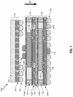
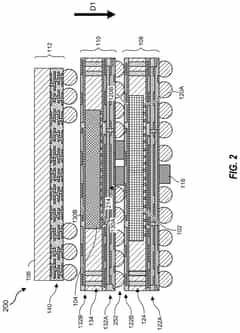
Chiplet arrangement
PatentActiveEP4451135A1
Innovation
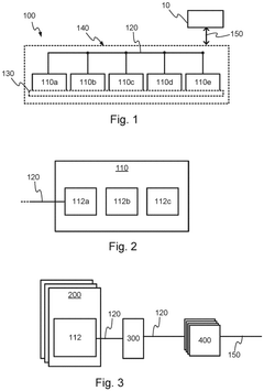
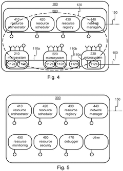
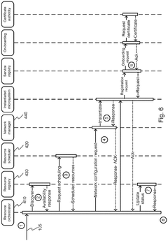
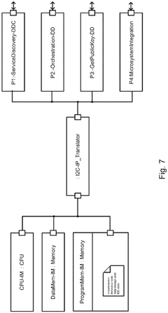
- A chiplet arrangement with a control plane that orchestrates microsystems and microservices, allowing for dynamic instantiation based on hardware resource availability and utilization, featuring a resource orchestrator, network manager, and resource scheduler to optimize resource utilization, scalability, and power management.
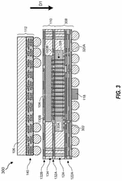
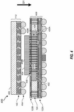
3D chiplet integration using fan-out wafer-level packaging
PatentPendingUS20240274587A1
Innovation
- The use of fan-out wafer-level packaging and three-dimensional packaging techniques for combining semiconductor chips and embedded memory in configurations such as face-to-back, back-to-back, and face-to-face orientations, enabling direct connections between chiplets and reducing assembly package sizes and manufacturing complexity.
Industry Standards and Interoperability Frameworks
The evolution of chiplet technology has necessitated the development of robust industry standards and interoperability frameworks to ensure seamless integration across different vendors and technologies. The Universal Chiplet Interconnect Express (UCIe) has emerged as a pivotal standard, establishing specifications for die-to-die interconnects that enable chiplets from various manufacturers to communicate effectively. This consortium-backed standard addresses physical layer, protocol layer, and software stack requirements, creating a foundation for a truly open chiplet ecosystem.
Beyond UCIe, the Advanced Interface Bus (AIB) developed by Intel provides another standardized approach for chiplet communication, focusing on high-bandwidth, low-latency connections between dies. Similarly, TSMC's Integrated Fan-Out (InFO) and Intel's Embedded Multi-die Interconnect Bridge (EMIB) represent packaging technologies that have established de facto standards in the industry for chiplet integration.
The Open Compute Project (OCP) has also contributed significantly to standardization efforts through its Open Domain-Specific Architecture (ODSA) subproject, which aims to create an open chiplet marketplace with standardized interfaces. This initiative promotes vendor-neutral specifications that enable mix-and-match capabilities across different chiplet providers.
Interoperability testing frameworks have become increasingly important as the chiplet ecosystem expands. Organizations like JEDEC and IEEE have developed testing methodologies and compliance programs to ensure that chiplets from different vendors can work together reliably. These frameworks include electrical validation, thermal performance verification, and system-level integration testing protocols.
The Common Hardware for Interfaces, Processors and Systems (CHIPS) Alliance, backed by the Linux Foundation, represents another collaborative effort to create open-source building blocks for chiplet designs. This initiative focuses on developing standardized IP blocks, interconnect protocols, and verification tools that facilitate chiplet-based system development.
Standardization efforts extend beyond hardware to include software abstraction layers that manage chiplet-based systems. The Heterogeneous System Architecture (HSA) Foundation has developed specifications for unified programming models that can address diverse computing elements within chiplet architectures, enabling software developers to efficiently utilize heterogeneous computing resources without needing to understand the underlying hardware complexity.
These evolving standards and frameworks collectively drive the chiplet ecosystem toward greater maturity, reducing integration risks and enabling broader adoption across the semiconductor industry. As these standards continue to develop, they will likely accelerate innovation by allowing companies to focus on their core competencies while leveraging the broader chiplet ecosystem.
Supply Chain Implications for Chiplet Ecosystem
The chiplet ecosystem represents a fundamental shift in semiconductor manufacturing, creating complex interdependencies across the global supply chain. The transition from monolithic designs to disaggregated chiplet architectures necessitates a reconfiguration of traditional semiconductor supply chains, introducing both challenges and opportunities for industry participants.
Material sourcing for chiplet production requires greater coordination among multiple suppliers, as different chiplets may utilize varying process nodes and manufacturing techniques. This diversification can reduce dependency on single-source suppliers but simultaneously increases supply chain complexity. Companies must develop sophisticated supplier management systems to track component compatibility and ensure consistent quality across multiple vendors.
Manufacturing logistics become particularly critical in chiplet integration, as production delays in any single component can disrupt the entire assembly process. The need for precise timing in component availability has driven the adoption of just-in-time manufacturing practices specifically tailored to chiplet production schedules. Industry leaders are establishing regional manufacturing clusters to minimize transportation delays and reduce geopolitical risks.
Testing and validation processes within the supply chain require significant enhancement for chiplet-based designs. Each chiplet must undergo individual testing before integration, followed by comprehensive system-level testing post-assembly. This multi-stage quality assurance process demands new equipment investments and specialized expertise throughout the supply chain.
Intellectual property management presents another supply chain consideration, as chiplet designs often incorporate IP from multiple sources. Clear licensing frameworks and standardized interfaces are becoming essential to facilitate seamless collaboration among ecosystem participants while protecting proprietary technologies.
Inventory management strategies are evolving to accommodate the modular nature of chiplet designs. Companies are developing flexible stocking approaches that balance the benefits of component reusability across multiple products against the costs of maintaining diverse chiplet inventories. This balance becomes particularly important as chiplet standards continue to evolve.
Geopolitical factors increasingly influence chiplet supply chain decisions, with companies pursuing geographic diversification to mitigate regional disruption risks. The establishment of parallel supply chains across different regions represents a strategic response to trade tensions and national security concerns surrounding semiconductor technologies.
Unlock deeper insights with Patsnap Eureka Quick Research — get a full tech report to explore trends and direct your research. Try now!
Generate Your Research Report Instantly with AI Agent
Supercharge your innovation with Patsnap Eureka AI Agent Platform!