Exploring the Synergy of Chiplet Integration and Industry Standards
OCT 15, 20259 MIN READ
Generate Your Research Report Instantly with AI Agent
Patsnap Eureka helps you evaluate technical feasibility & market potential.
Chiplet Technology Evolution and Integration Goals
The evolution of chiplet technology represents a paradigm shift in semiconductor design and manufacturing, moving away from monolithic system-on-chip (SoC) approaches toward modular integration of specialized silicon dies. This transition began in the early 2010s as semiconductor scaling challenges became increasingly apparent, with Moore's Law facing physical and economic limitations. The industry recognized that continuing to integrate more functionality onto a single die was becoming prohibitively expensive and technically challenging, particularly at advanced nodes below 7nm.
Chiplet architecture emerged as a strategic response to these challenges, allowing semiconductor companies to decompose complex systems into smaller functional blocks that could be manufactured using optimal process technologies for each component. This approach enables mixing of mature and cutting-edge process nodes on a single package, optimizing for performance, power, and cost considerations.
The evolution trajectory has progressed from simple multi-chip modules (MCMs) to sophisticated 2.5D and 3D integration schemes utilizing advanced packaging technologies such as silicon interposers, fan-out wafer-level packaging (FOWLP), and through-silicon vias (TSVs). Each advancement has enabled higher bandwidth, lower latency, and more efficient power delivery between chiplets, progressively removing the performance penalties associated with disaggregation.
Key technological milestones include AMD's introduction of Infinity Fabric in 2017, Intel's EMIB (Embedded Multi-die Interconnect Bridge) and Foveros technologies, and TSMC's CoWoS (Chip on Wafer on Substrate) platform. These innovations have demonstrated the commercial viability of chiplet-based designs in high-performance computing applications.
The primary integration goals for chiplet technology center around establishing standardized interfaces and protocols that enable interoperability between chiplets from different vendors. This includes developing unified die-to-die interconnect standards, common physical and logical interfaces, and standardized testing methodologies. The ultimate objective is to create a robust chiplet ecosystem where specialized components can be sourced from multiple suppliers and integrated seamlessly, similar to how printed circuit boards allow for component-level integration today.
Additional integration goals include reducing the design complexity associated with heterogeneous integration, improving thermal management across multiple dies, enhancing yield through known-good-die testing, and developing sophisticated design tools that can optimize system-level performance across chiplet boundaries. The industry also aims to establish supply chain models that support this disaggregated approach to semiconductor design and manufacturing.
Market Demand Analysis for Chiplet-Based Solutions
The global chiplet market is experiencing unprecedented growth, driven by the increasing demand for high-performance computing solutions across various industries. According to recent market analyses, the chiplet technology market is projected to grow at a CAGR of 40% from 2023 to 2030, reaching significant market valuation as computing demands continue to escalate. This remarkable growth trajectory is primarily fueled by the limitations of traditional monolithic chip designs in meeting the performance requirements of emerging applications.
Data centers and cloud service providers represent the largest market segment for chiplet-based solutions, accounting for approximately 45% of the current demand. These entities require increasingly powerful processing capabilities to handle massive data workloads, AI training, and inference operations. The ability of chiplet technology to deliver higher performance while managing power consumption and thermal issues makes it particularly attractive for hyperscale deployments.
The telecommunications sector, especially with the ongoing global 5G rollout and preparation for 6G technologies, constitutes the second-largest market segment. Network infrastructure providers are actively seeking chiplet-based solutions to address the computational demands of next-generation communication systems while maintaining energy efficiency and physical space constraints.
Consumer electronics manufacturers are rapidly adopting chiplet technology for high-end products, particularly in gaming consoles, premium smartphones, and AR/VR devices. Market research indicates that consumer awareness of processing power as a differentiating factor has increased by 35% over the past three years, creating pull-through demand for advanced semiconductor solutions.
The automotive industry represents an emerging but rapidly growing market for chiplet technology. Advanced driver-assistance systems (ADAS), autonomous driving capabilities, and in-vehicle infotainment systems require substantial computing power in constrained environments. Industry forecasts suggest that the automotive chiplet market segment will grow at nearly 50% annually through 2028, outpacing most other sectors.
Industrial automation and IoT applications are creating additional demand vectors for chiplet-based solutions. The need for edge computing capabilities in industrial settings, combined with stringent requirements for reliability and longevity, makes chiplet technology particularly suitable for these applications. Market penetration in this segment is expected to triple over the next five years.
A critical market driver is the industry-wide push toward standardization of chiplet interfaces and integration methodologies. Organizations adopting open standards like UCIe (Universal Chiplet Interconnect Express) are experiencing 30% faster time-to-market for new products compared to those using proprietary interfaces, creating strong economic incentives for standardization across the ecosystem.
Current Challenges in Chiplet Integration Standards
Despite significant advancements in chiplet integration technologies, the industry faces several critical challenges in standardization that impede broader adoption and interoperability. The fragmentation of existing standards represents a primary obstacle, with multiple competing frameworks such as UCIe (Universal Chiplet Interconnect Express), AIB (Advanced Interface Bus), and BoW (Bunch of Wires) creating a complex landscape for manufacturers and designers. This fragmentation forces companies to make strategic bets on which standards will prevail, potentially leading to stranded investments if market adoption shifts unexpectedly.
Interoperability between chiplets from different vendors remains problematic due to inconsistent implementation of interface protocols. While UCIe has emerged as a promising standard with backing from major industry players including Intel, AMD, and TSMC, full compatibility across the ecosystem has not yet been achieved. The technical specifications for physical layer connections, power management, and thermal considerations still vary significantly between implementations, creating integration challenges for system designers.
Testing and validation methodologies present another significant hurdle. Unlike traditional monolithic chips with established testing procedures, chiplet-based designs require new approaches to verify functionality across die boundaries. The industry lacks standardized testing protocols that can effectively validate the performance and reliability of inter-chiplet connections, particularly when components come from different manufacturers with varying quality assurance practices.
Intellectual property (IP) protection and licensing frameworks remain underdeveloped for chiplet ecosystems. The business models for sharing and licensing chiplet designs across companies are still evolving, creating uncertainty around how IP rights are managed when multiple vendors contribute to a single package. This uncertainty discourages some potential market participants from fully embracing chiplet-based approaches.
Supply chain coordination represents a complex challenge that extends beyond technical considerations. Chiplet integration requires precise alignment of manufacturing processes, packaging technologies, and delivery timelines across multiple suppliers. Without standardized approaches to supply chain management specific to chiplet ecosystems, companies face increased risks of production delays and quality inconsistencies.
Security considerations for chiplet-based systems remain inadequately addressed in current standards. The increased number of interfaces between components creates potential new attack vectors that traditional security models may not fully account for. Standards bodies are only beginning to develop comprehensive security frameworks that address the unique vulnerabilities of disaggregated chip architectures.
Thermal management across chiplet interfaces presents technical challenges that current standards do not fully resolve. The heat dissipation characteristics at die boundaries can significantly impact overall system performance, yet standardized approaches to thermal design for multi-die packages are still evolving, creating uncertainty for system integrators.
Existing Chiplet Integration Methodologies
01 Standardized Chiplet Interfaces and Protocols
Standardized interfaces and protocols are essential for enabling interoperability between chiplets from different manufacturers. These standards define the physical and logical connections between chiplets, including signal integrity, power delivery, and communication protocols. By adhering to industry standards, chiplet designs can be more easily integrated into complex systems, reducing development time and costs while ensuring compatibility across different platforms.- Standardized Chiplet Interfaces and Protocols: Standardized interfaces and protocols are essential for successful chiplet integration across the industry. These standards enable different chiplets from various manufacturers to communicate effectively, ensuring interoperability. The development of common electrical and physical interfaces allows for modular design approaches where chiplets can be mixed and matched regardless of their origin. These standards typically define signal integrity requirements, power delivery specifications, and communication protocols that facilitate seamless integration.
- Advanced Packaging Technologies for Chiplet Integration: Advanced packaging technologies are crucial for effective chiplet integration, enabling high-density interconnects between different chiplet components. These technologies include 2.5D and 3D integration methods, silicon interposers, and through-silicon vias (TSVs) that facilitate the close coupling of multiple chiplets in a single package. The packaging solutions address thermal management challenges, signal integrity issues, and power distribution concerns that arise when integrating multiple chiplets with different functionalities and from different process nodes.
- Collaborative Industry Ecosystems for Chiplet Development: Collaborative industry ecosystems are forming to accelerate chiplet technology development and standardization. These collaborations involve semiconductor manufacturers, equipment suppliers, design tool vendors, and end-users working together to establish common frameworks for chiplet design, manufacturing, and integration. Industry consortia are developing shared intellectual property, design methodologies, and verification procedures to reduce barriers to chiplet adoption and enable a more diverse and competitive chiplet marketplace.
- Design Automation and Verification Tools for Chiplet Systems: Specialized design automation and verification tools are being developed to address the unique challenges of chiplet-based system design. These tools support the modeling and simulation of multi-chiplet systems, including the analysis of thermal, electrical, and mechanical interactions between chiplets. Advanced verification methodologies ensure that chiplets from different sources will function correctly when integrated. The tools also facilitate the optimization of chiplet placement and routing to maximize performance while minimizing power consumption and latency.
- Heterogeneous Integration and Optimization Techniques: Heterogeneous integration techniques enable the combination of chiplets manufactured using different process technologies, optimizing each component for its specific function. This approach allows for the integration of analog, RF, memory, and digital processing chiplets in a single package, each fabricated using the most appropriate technology node. Advanced optimization techniques balance performance, power, and cost considerations across the entire chiplet-based system, enabling customized solutions for specific application requirements while maintaining manufacturing efficiency.
02 Advanced Packaging Technologies for Chiplet Integration
Advanced packaging technologies play a crucial role in chiplet integration by providing the physical infrastructure for connecting multiple chiplets. These technologies include 2.5D and 3D integration methods, interposers, and through-silicon vias (TSVs). The packaging solutions must address thermal management, signal integrity, and power delivery challenges while maintaining high performance and reliability. Innovations in this area focus on reducing the physical footprint while increasing the density of interconnections between chiplets.Expand Specific Solutions03 System-Level Design and Verification for Chiplet-Based Architectures
System-level design and verification methodologies are critical for ensuring the proper functioning of chiplet-based architectures. These methodologies include simulation, emulation, and formal verification techniques that validate the interaction between chiplets before physical implementation. Design tools and frameworks that support chiplet integration must account for the unique challenges of multi-die systems, including timing closure, power management, and testing strategies across chiplet boundaries.Expand Specific Solutions04 Chiplet-Based Computing Architectures and Performance Optimization
Chiplet-based computing architectures offer new approaches to system design by disaggregating traditional monolithic chips into specialized functional blocks. These architectures enable mixing and matching of chiplets with different process technologies, optimizing for performance, power, and cost. Innovations in this area include memory-compute integration, accelerator chiplets for specific workloads, and novel interconnect topologies that minimize latency and maximize bandwidth between chiplets.Expand Specific Solutions05 Industry Collaboration and Ecosystem Development for Chiplet Standards
Industry collaboration and ecosystem development are fundamental to the success of chiplet integration. This includes the formation of industry consortia, development of reference designs, and creation of testing and certification processes. By working together, semiconductor companies, foundries, and system integrators can establish common standards that enable a robust chiplet marketplace. These collaborative efforts focus on defining technical specifications, business models, and intellectual property frameworks that support the chiplet ecosystem.Expand Specific Solutions
Key Industry Players in Chiplet Ecosystem
The chiplet integration market is currently in a growth phase, characterized by increasing adoption across the semiconductor industry. The market size is expanding rapidly as chiplet technology addresses scaling challenges in traditional monolithic designs. Leading players include Intel, AMD, and TSMC, who have established strong positions through advanced packaging technologies and industry standards development. Qualcomm and Micron are leveraging chiplet integration for mobile and memory applications, while SMIC and GlobalFoundries are building capabilities to compete in this space. Technical maturity varies significantly, with Intel's EMIB and Foveros, AMD's Infinity Fabric, and TSMC's CoWoS and InFO technologies representing the most advanced implementations. The industry is moving toward standardization through initiatives like UCIe, with Huawei and Bosch also contributing to ecosystem development.
Taiwan Semiconductor Manufacturing Co., Ltd.
Technical Solution: TSMC has developed advanced packaging technologies specifically designed for chiplet integration, including their CoWoS (Chip-on-Wafer-on-Substrate), InFO (Integrated Fan-Out), and SoIC (System on Integrated Chips) platforms. Their CoWoS technology enables the integration of multiple chiplets on a silicon interposer with high-density interconnects, widely used for high-performance computing applications. SoIC represents TSMC's most advanced 3D integration technology, allowing for chip stacking with extremely fine pitch connections. TSMC has established their 3DFabric platform as a comprehensive integration architecture that combines front-end and back-end technologies to enable various chiplet designs. As a founding member of the UCIe consortium, TSMC is actively working to ensure their manufacturing processes align with emerging industry standards while offering customers specialized integration options[5]. Their Advanced Backend Factory (ABF) focuses specifically on advanced packaging technologies, demonstrating their commitment to chiplet-based architectures as a strategic direction.
Strengths: As the world's leading semiconductor foundry, TSMC offers unmatched manufacturing capabilities and process technologies that enable cutting-edge chiplet designs. Their neutral position as a manufacturer allows them to support multiple competing standards and architectures. Weaknesses: They must balance the interests of numerous customers who may have competing chiplet strategies, and their role is primarily as an enabler rather than defining the standards themselves.
QUALCOMM, Inc.
Technical Solution: Qualcomm has embraced chiplet architecture in their mobile and edge computing platforms through their Snapdragon system-on-chip designs. Their approach focuses on heterogeneous integration, combining specialized processing elements (CPU, GPU, DSP, NPU) as separate chiplets optimized for mobile power constraints. Qualcomm's chiplet strategy emphasizes their proprietary NoC (Network-on-Chip) interconnect technology that provides high-bandwidth, low-latency communication between chiplets while minimizing power consumption. Their recent Snapdragon X Elite platform demonstrates advanced chiplet integration by combining their custom Oryon CPU cores with dedicated neural processing units and graphics processors. Qualcomm has joined the UCIe consortium while continuing to develop their own interconnect technologies optimized for mobile applications[6]. Their acquisition of NUVIA has accelerated their custom CPU development, allowing for more specialized chiplet designs targeting specific performance and power envelopes across mobile, automotive, and edge computing applications.
Strengths: Qualcomm's expertise in power-efficient designs gives them advantages in implementing chiplet architectures for mobile and battery-powered applications. Their vertical integration of design and IP allows for highly optimized interconnect solutions. Weaknesses: Their focus on mobile applications may limit their influence on broader data center and high-performance computing standards, and they face increasing competition from custom silicon designs from companies like Apple.
Core Patents and Technical Innovations in Chiplet Design
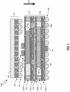
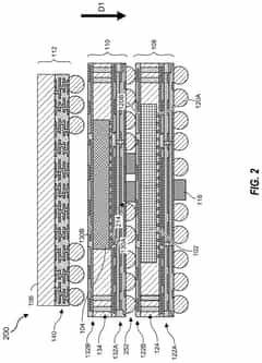
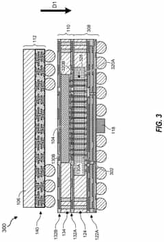
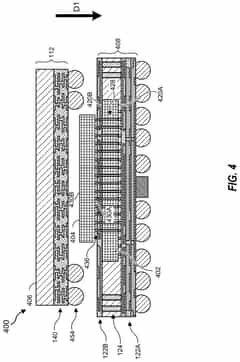
3D chiplet integration using fan-out wafer-level packaging
PatentPendingUS20240274587A1
Innovation
- The use of fan-out wafer-level packaging and three-dimensional packaging techniques for combining semiconductor chips and embedded memory in configurations such as face-to-back, back-to-back, and face-to-face orientations, enabling direct connections between chiplets and reducing assembly package sizes and manufacturing complexity.
Integrated Artificial Intelligence Based Material Selection for Industrial Assets
PatentPendingUS20250244752A1
Innovation
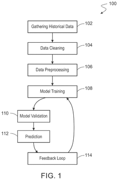
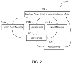
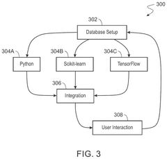
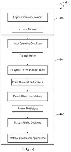
- An AI-driven method that integrates historical data with industry standards to train machine learning models, predicting material performance and ensuring compliance with safety and durability criteria, using supervised learning techniques like Support Vector Machines and Decision Trees, and incorporating feedback loops for continuous improvement.
Interoperability Framework for Cross-Vendor Chiplets
The establishment of an interoperability framework for cross-vendor chiplets represents a critical milestone in the evolution of chiplet technology. This framework aims to create standardized interfaces, protocols, and methodologies that enable chiplets from different manufacturers to seamlessly integrate and function together within a single package. The foundation of such a framework rests on three key pillars: physical interconnect standardization, protocol compatibility, and power/thermal management coordination.
Physical interconnect standardization focuses on defining uniform die-to-die interfaces that ensure mechanical and electrical compatibility across different vendors' chiplets. This includes standardizing bump pitches, pad layouts, and signal integrity requirements to facilitate reliable connections between heterogeneous components. Organizations like the Universal Chiplet Interconnect Express (UCIe) consortium have made significant progress in this area, establishing specifications for both die-to-die and package-to-package interconnects.
Protocol compatibility addresses the need for common communication protocols that enable efficient data exchange between chiplets regardless of their origin. This involves standardizing transaction layers, data encoding schemes, and flow control mechanisms. The Advanced Interface Bus (AIB), Bunch of Wires (BoW), and OpenHBI are emerging as potential industry standards in this domain, each offering different trade-offs between performance, power efficiency, and implementation complexity.
Power and thermal management coordination ensures that chiplets from different vendors can operate within a unified power delivery network and thermal solution. This requires standardized approaches to power state transitions, thermal monitoring, and dynamic thermal management. The framework must define clear interfaces for communicating power and thermal information between chiplets and the system controller.
Testing and validation methodologies constitute another crucial aspect of the interoperability framework. Standardized test procedures and compliance verification methods are essential to ensure that chiplets from different vendors can be certified as compatible with the framework. This includes both pre-integration validation and post-integration system-level testing protocols.
The governance model for maintaining and evolving the interoperability framework presents significant challenges. Industry consortia like CHIPS Alliance, OCP, and UCIe are working to establish collaborative governance structures that balance innovation with stability. The framework must be flexible enough to incorporate technological advancements while maintaining backward compatibility with existing chiplet designs.
Intellectual property considerations also play a vital role in the framework's development. Clear licensing models and IP protection mechanisms are necessary to encourage widespread adoption while respecting proprietary technologies. The industry is moving toward a combination of open standards for basic interconnect specifications and licensed technologies for advanced features.
Economic Impact of Standardized Chiplet Adoption
The standardization of chiplet interfaces and integration methodologies represents a significant economic inflection point for the semiconductor industry. As chiplet technology matures from proprietary implementations to industry-wide standards, the economic implications extend far beyond individual manufacturers to reshape the entire semiconductor value chain.
The adoption of standardized chiplet interfaces such as UCIe (Universal Chiplet Interconnect Express) is projected to reduce development costs by 25-40% compared to monolithic SoC designs. This cost reduction stems primarily from the ability to mix and match pre-validated chiplet components, eliminating redundant design efforts and leveraging economies of scale across multiple product lines.
Manufacturing economics also transform substantially under standardized chiplet paradigms. The ability to produce smaller dies on optimal process nodes increases yield rates by an estimated 15-30%, particularly for cutting-edge processes where defect density significantly impacts production economics. This yield improvement translates directly to lower per-unit costs and higher margins for semiconductor companies.
The chiplet ecosystem further democratizes access to advanced semiconductor capabilities. Smaller design houses and specialized IP vendors can now participate in high-performance computing markets previously dominated by vertically integrated giants. Market analysis indicates this ecosystem expansion could generate $25-35 billion in new semiconductor revenue by 2028, representing approximately 5% of the projected total semiconductor market.
Supply chain resilience improves markedly with standardized chiplets. The modular nature of chiplet-based designs allows manufacturers to diversify production across multiple foundries and geographies, reducing dependency on single sources. Economic modeling suggests this could reduce supply disruption risks by 30-45%, a critical consideration given recent global supply chain vulnerabilities.
Time-to-market acceleration represents another substantial economic benefit. Products utilizing standardized chiplet interfaces demonstrate 40-60% faster development cycles compared to traditional approaches. This acceleration creates significant competitive advantages and allows companies to capture premium pricing during early market windows.
The standardization of chiplets also drives significant capital efficiency improvements. Rather than investing in comprehensive capabilities across all semiconductor processes, companies can focus capital expenditures on their areas of differentiation while sourcing complementary capabilities through the chiplet ecosystem. Industry analysts project this could reduce capital requirements by 30-50% for new semiconductor product lines.
Unlock deeper insights with Patsnap Eureka Quick Research — get a full tech report to explore trends and direct your research. Try now!
Generate Your Research Report Instantly with AI Agent
Supercharge your innovation with Patsnap Eureka AI Agent Platform!