

How Is Chiplet Integration Affecting Product Compliance Standards
OCT 15, 20259 MIN READ
Generate Your Research Report Instantly with AI Agent
PatSnap Eureka helps you evaluate technical feasibility & market potential.
Chiplet Integration Background and Objectives
Chiplet integration represents a paradigm shift in semiconductor design and manufacturing, evolving from the traditional monolithic system-on-chip (SoC) approach to a more modular architecture. This evolution began in the early 2010s as semiconductor manufacturers faced increasing challenges with Moore's Law, where the economic and technical feasibility of shrinking transistors became progressively more difficult. The concept of disaggregating large silicon dies into smaller, specialized chiplets emerged as a strategic response to these challenges.
The historical trajectory of chiplet technology can be traced through several key milestones. AMD's introduction of their Infinity Fabric interconnect in 2017 marked one of the first commercial implementations, allowing the company to connect multiple silicon dies within a single package. Intel followed with their Embedded Multi-die Interconnect Bridge (EMIB) and later Foveros technology, while TSMC developed their Integrated Fan-Out (InFO) and System on Integrated Chips (SoIC) technologies.
The primary objective of chiplet integration is to overcome the limitations of monolithic chip design while maintaining performance improvements. By separating a complex system into smaller, specialized dies manufactured using optimal process nodes, companies can achieve better yields, reduced costs, and enhanced flexibility in product development. This approach allows for mixing and matching different process technologies within a single package, optimizing each component for its specific function.
From a compliance perspective, the objectives include establishing standardized interfaces between chiplets to ensure interoperability across different manufacturers. Organizations such as the Universal Chiplet Interconnect Express (UCIe) consortium are working to develop open specifications for die-to-die interconnects, which is crucial for the broader adoption of chiplet technology across the industry.
The technology trend clearly points toward increasing heterogeneous integration, with chiplets becoming smaller, more specialized, and interconnected through increasingly sophisticated packaging technologies. This trend is driven by the need for continued performance scaling despite the slowing of traditional node shrinking, as well as the economic benefits of improved yields and reduced development costs.
Looking forward, the chiplet approach aims to enable a more diverse ecosystem where specialized manufacturers can focus on their core competencies while still participating in the creation of complex integrated systems. This represents a fundamental shift in how semiconductor products are designed, manufactured, and brought to market, with significant implications for product compliance standards across the industry.
Market Demand Analysis for Chiplet-Based Products
The chiplet market is experiencing unprecedented growth, driven by the increasing demand for high-performance computing solutions across multiple industries. Current market analysis indicates that the global chiplet market is projected to grow at a compound annual growth rate of 40% between 2023 and 2028, reaching approximately 50 billion dollars by the end of this period. This remarkable growth trajectory is primarily fueled by the semiconductor industry's shift away from traditional monolithic designs toward more modular and efficient architectures.
Data center operators represent the largest market segment for chiplet-based products, as they continuously seek solutions that offer improved performance, reduced power consumption, and enhanced thermal management. The demand from this sector is expected to grow by 35% annually as hyperscalers and cloud service providers upgrade their infrastructure to meet escalating computational requirements while managing operational costs.
Consumer electronics manufacturers constitute the second-largest market segment, with particular interest in chiplet solutions that enable more powerful yet energy-efficient mobile devices, laptops, and gaming systems. Market research indicates that approximately 30% of premium consumer electronics will incorporate chiplet-based processors by 2025, up from less than 10% in 2022.
The automotive industry is emerging as a rapidly growing market for chiplet technology, particularly for advanced driver-assistance systems (ADAS) and autonomous driving platforms. Industry forecasts suggest that chiplet adoption in automotive applications will grow by 45% annually over the next five years, as manufacturers seek to integrate more computing power into vehicles while meeting stringent reliability and safety standards.
Telecommunications equipment manufacturers are increasingly turning to chiplet-based solutions for 5G and future 6G infrastructure, with market penetration expected to reach 25% by 2026. This sector values the scalability and performance advantages that chiplet architectures offer for network processing units and base station equipment.
From a geographical perspective, North America currently leads in chiplet adoption, accounting for approximately 40% of the global market, followed by Asia-Pacific at 35% and Europe at 20%. However, the Asia-Pacific region is expected to show the highest growth rate over the next five years, potentially overtaking North America as the largest market by 2027.
Customer surveys indicate that while performance improvements remain the primary driver for chiplet adoption, concerns about compliance with evolving standards and interoperability between different vendors' chiplets are significant factors influencing purchasing decisions. Approximately 65% of potential enterprise customers cite standardization concerns as a major consideration in their technology roadmap planning.
Current Compliance Challenges in Chiplet Technology
The integration of chiplet technology into semiconductor manufacturing has introduced unprecedented compliance challenges that extend beyond traditional monolithic chip designs. As chiplets represent disaggregated components from potentially different manufacturers, ensuring uniform compliance across the entire system becomes exponentially more complex. Current regulatory frameworks were largely developed for single-die architectures, creating significant gaps in addressing multi-die implementations.
Interoperability standards represent one of the most pressing compliance challenges. With chiplets from various vendors needing to communicate seamlessly, the industry faces difficulties in establishing universal protocols for die-to-die interfaces. The lack of standardized testing methodologies for these interfaces further complicates compliance verification, as traditional boundary scan techniques prove insufficient for chiplet-based architectures.
Thermal management compliance has emerged as another critical concern. The dense packaging of multiple chiplets creates thermal hotspots and complex heat dissipation patterns that existing thermal compliance standards fail to adequately address. Current thermal testing protocols typically assume uniform heat distribution across a single die, whereas chiplet designs exhibit highly variable thermal profiles depending on the specific arrangement and operational states of individual dies.
Security compliance frameworks face significant challenges with chiplet integration. The increased number of physical interfaces between dies creates additional attack vectors that traditional security compliance testing may not detect. Moreover, when chiplets from different vendors are combined, establishing end-to-end security compliance becomes problematic due to varying security implementations and potential incompatibilities between security protocols.
Electromagnetic compatibility (EMC) standards are also struggling to keep pace with chiplet technology. The multiple high-speed interfaces between chiplets generate complex electromagnetic interference patterns that can affect both internal system operation and external devices. Current EMC testing methodologies often fail to accurately characterize these interactions, leading to potential compliance gaps.
Supply chain compliance represents another significant hurdle. With components potentially sourced from multiple global vendors, ensuring consistent compliance with various regional regulations becomes increasingly difficult. This is particularly challenging for industries with strict traceability requirements, such as automotive, medical, and aerospace sectors, where component-level certification is often mandatory.
The fragmented nature of compliance responsibilities between chiplet suppliers and system integrators creates additional complexity. Questions regarding which party bears ultimate responsibility for system-level compliance remain largely unresolved, creating potential liability issues and market uncertainties that could impede broader chiplet adoption.
Current Compliance Standards and Testing Methodologies
01 Chiplet integration compliance frameworks
Compliance frameworks for chiplet integration establish standardized protocols and requirements that ensure interoperability between different chiplet components. These frameworks define electrical, physical, and logical interfaces that chiplets must adhere to for successful integration. By following these standards, manufacturers can ensure that chiplets from different vendors can work together seamlessly in a single package, reducing integration challenges and improving time-to-market.- Standardization frameworks for chiplet integration: Standardization frameworks establish common protocols and interfaces for chiplet integration, ensuring interoperability between different chiplet components. These frameworks define electrical, physical, and logical interfaces that chiplets must adhere to for successful integration. By following these standards, manufacturers can ensure that chiplets from different vendors can work together seamlessly in a single package, reducing integration challenges and improving time-to-market.
- Compliance testing methodologies for chiplet interfaces: Compliance testing methodologies are essential for verifying that chiplet interfaces meet the required standards. These methodologies include automated testing procedures, validation protocols, and certification processes that ensure chiplets conform to industry standards. Testing covers signal integrity, power delivery, thermal performance, and functional verification to guarantee reliable operation when chiplets are integrated into a system.
- Regulatory compliance for chiplet-based products: Chiplet-based products must comply with various regulatory requirements across different markets. This includes electromagnetic compatibility standards, safety regulations, and environmental compliance such as RoHS and REACH. Manufacturers need to implement processes to track and document compliance throughout the product lifecycle, from design and manufacturing to distribution and disposal, ensuring that integrated chiplet products meet all applicable legal requirements.
- Quality management systems for chiplet integration: Quality management systems provide structured approaches to ensure consistent quality in chiplet integration processes. These systems include documentation requirements, process controls, and continuous improvement methodologies specific to chiplet manufacturing and integration. By implementing robust quality management systems, manufacturers can minimize defects, improve yield rates, and ensure that integrated chiplet products meet performance and reliability standards.
- Intellectual property management for chiplet ecosystems: Intellectual property management is crucial in the chiplet ecosystem where multiple vendors may contribute different components. This includes licensing frameworks, patent pools, and IP compliance verification systems that enable collaboration while protecting proprietary technologies. Effective IP management ensures that all chiplet components in an integrated product have proper licensing and that potential patent infringement risks are mitigated before products reach the market.
02 Testing and validation standards for chiplet-based systems
Testing and validation standards specific to chiplet-based systems ensure that integrated chiplets meet performance, reliability, and compatibility requirements. These standards define test methodologies, validation procedures, and quality metrics that must be applied during development and manufacturing. Comprehensive testing frameworks help identify integration issues early in the development cycle and ensure that chiplet-based products comply with industry standards before market release.Expand Specific Solutions03 Intellectual property management for chiplet ecosystems
Standards for intellectual property management in chiplet ecosystems address the complex IP landscape when integrating components from multiple vendors. These standards establish protocols for IP protection, licensing frameworks, and compliance verification mechanisms. By providing clear guidelines for IP handling, these standards facilitate collaboration between chiplet providers while protecting proprietary technologies and ensuring that integrated products comply with all relevant IP agreements.Expand Specific Solutions04 Security compliance standards for chiplet integration
Security compliance standards for chiplet integration focus on ensuring that integrated chiplet systems maintain data integrity, confidentiality, and protection against security threats. These standards define security requirements for inter-chiplet communication, authentication mechanisms, and secure boot processes. Compliance with these security standards is critical for chiplet-based products in sensitive applications such as financial services, healthcare, and government systems.Expand Specific Solutions05 Regulatory compliance for chiplet-based products
Regulatory compliance standards for chiplet-based products ensure that integrated systems meet regional and international regulations regarding electromagnetic compatibility, power consumption, environmental impact, and other regulatory requirements. These standards provide guidelines for documentation, certification processes, and compliance testing that manufacturers must follow. Adhering to these regulatory standards is essential for global market access and avoiding legal issues related to non-compliance.Expand Specific Solutions
Key Industry Players in Chiplet Integration Ecosystem
Chiplet integration is reshaping product compliance standards in a rapidly evolving semiconductor landscape. The industry is transitioning from traditional monolithic designs to modular chiplet architectures, with market growth projected to reach $57 billion by 2035. While still in early maturity stages, major players are advancing at different rates. TSMC, Intel, and AMD lead with established chiplet technologies, while Samsung, SMIC, and Micron are accelerating investments. Qualcomm and IBM focus on standardization efforts through UCIe consortium. Compliance challenges center around interoperability, thermal management, and signal integrity across heterogeneous integration, requiring new testing methodologies and standards harmonization across global markets.
Taiwan Semiconductor Manufacturing Co., Ltd.
Technical Solution: TSMC has developed its Integrated Fan-Out (InFO) and System on Integrated Chips (SoIC) technologies to address chiplet integration challenges. Their approach emphasizes 3D integration with through-silicon vias (TSVs) and chip-on-wafer-on-substrate (CoWoS) packaging. For compliance standards, TSMC has implemented a comprehensive chiplet validation methodology that includes advanced signal integrity testing across die-to-die interfaces. Their compliance framework addresses thermal challenges through innovative heat dissipation solutions specifically designed for densely packed chiplet configurations. TSMC has also developed specialized reliability testing protocols for their 3D stacking technologies, focusing on mechanical stress testing and thermal cycling to ensure long-term reliability. Their 3DFabric platform provides an integrated solution for chiplet-based designs, with standardized interfaces and validation methodologies that help customers meet regulatory requirements more efficiently. TSMC collaborates with customers to develop custom compliance testing procedures tailored to specific chiplet configurations.
Strengths: TSMC's advanced packaging technologies and manufacturing excellence provide superior integration capabilities. Their close partnerships with major semiconductor companies allow for collaborative compliance solutions. Weaknesses: Their proprietary interconnect technologies may face challenges as the industry moves toward open standards like UCIe, potentially requiring significant adaptation of compliance testing methodologies.
Intel Corp.
Technical Solution: Intel has pioneered chiplet integration through its Advanced Interface Bus (AIB) and Embedded Multi-die Interconnect Bridge (EMIB) technologies. Their approach focuses on disaggregating complex SoCs into smaller chiplets manufactured using optimal process nodes. Intel's Ponte Vecchio GPU exemplifies this strategy, incorporating over 40 chiplets using different process technologies. For compliance standards, Intel has implemented a comprehensive validation framework that addresses thermal management challenges through advanced cooling solutions and package-level thermal modeling. Their compliance strategy includes extensive electromagnetic interference (EMI) testing protocols specifically designed for multi-chiplet configurations, as the increased number of high-speed interconnects between chiplets can create new EMI challenges. Intel also leads industry standardization efforts through the Universal Chiplet Interconnect Express (UCIe) consortium, which aims to establish open standards for die-to-die interconnects.
Strengths: Intel's established manufacturing infrastructure and extensive experience with heterogeneous integration provide significant advantages in meeting compliance standards. Their leadership in UCIe standardization efforts positions them favorably in the ecosystem. Weaknesses: The complexity of their multi-chiplet designs increases validation time and costs, potentially slowing time-to-market compared to monolithic approaches.
Critical Patents and Technical Literature on Chiplet Compliance
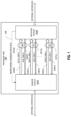
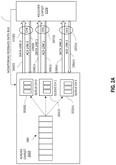
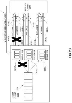
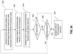
Techniques for resiliency in automotive-grade chiplets
PatentActiveUS20240166147A1
Innovation
- The implementation of a monitoring feedback data bus between chiplets for continuous health monitoring, error detection, and automatic switching to backup channels, along with sequence numbers and cyclic redundancy checks, enables efficient error handling and data transmission across multiple channels, ensuring reliable communication and resilience.
Low-latency register error correction
PatentActiveUS20230101219A1
Innovation
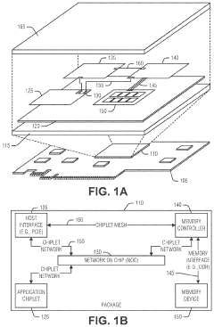
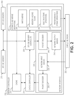
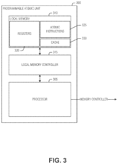
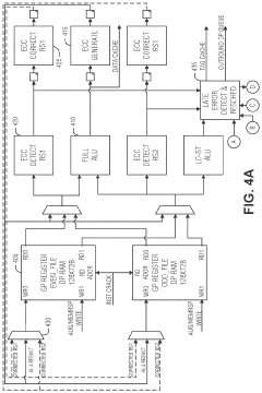
- The implementation of a programmable atomic unit (PAU) within the memory controller chiplet that performs low-latency register error correction by changing the current instruction into a register update instruction when an error is detected, and using a credit-based flow control technique in the Chiplet Protocol Interface (CPI) to minimize latency and energy consumption in chiplet interconnects.
Regulatory Framework Evolution for Heterogeneous Integration
The regulatory landscape for heterogeneous integration technologies is undergoing significant transformation as chiplet-based designs become increasingly prevalent. Traditional compliance frameworks were developed for monolithic integrated circuits, creating a regulatory gap for multi-die packages that combine different process nodes, IP blocks, and potentially components from multiple vendors.
International standards bodies including IEEE, JEDEC, and ISO have begun developing specialized standards addressing the unique challenges of chiplet integration. The IEEE 2851 standard, focused on inter-chiplet interfaces, represents a critical step toward establishing uniform compliance requirements for heterogeneous systems. Similarly, JEDEC has expanded its JEP174 guidelines to incorporate testing methodologies specific to multi-die packages.
Regulatory agencies worldwide are adapting their certification processes to accommodate the complexity of chiplet-based products. The European Union's updated EMC Directive now includes specific provisions for heterogeneous integrated systems, recognizing that electromagnetic compatibility characteristics differ significantly from traditional monolithic designs. In the United States, the FCC has initiated a review of its certification requirements to better address the unique electromagnetic emission profiles of chiplet-based products.
Security and data protection regulations present particular challenges for chiplet integration. The distributed nature of processing in heterogeneous systems creates new attack vectors that existing regulatory frameworks may not adequately address. The EU's Cyber Resilience Act and similar initiatives in other jurisdictions are evolving to incorporate security requirements specific to multi-die architectures, including secure die-to-die communication channels and protection against side-channel attacks unique to chiplet implementations.
Supply chain regulations are also adapting to the chiplet paradigm. The CHIPS Act in the United States and similar initiatives globally now include provisions specifically addressing heterogeneous integration technologies, recognizing their strategic importance to semiconductor sovereignty. These frameworks increasingly require traceability and verification mechanisms for individual chiplets within integrated packages.
Thermal management and power efficiency standards are being revised to account for the unique thermal characteristics of chiplet-based designs. Energy efficiency regulations like Energy Star are developing new testing methodologies that consider the distributed power profiles of heterogeneous systems rather than applying monolithic benchmarking approaches.
As the regulatory framework continues to evolve, industry consortia like the Universal Chiplet Interconnect Express (UCIe) are working closely with regulatory bodies to develop standards that balance innovation with compliance requirements, ensuring that heterogeneous integration can advance while meeting increasingly complex regulatory demands across global markets.
Cross-Industry Standardization Efforts and Initiatives
The chiplet revolution has catalyzed unprecedented cross-industry collaboration, with multiple standardization bodies working to establish unified frameworks for this emerging technology. The Universal Chiplet Interconnect Express (UCIe) consortium represents one of the most significant standardization efforts, bringing together semiconductor giants like Intel, AMD, Arm, TSMC, and Samsung. UCIe focuses on establishing die-to-die interconnect standards that enable chiplets from different vendors to communicate seamlessly, addressing a critical interoperability challenge.
Parallel to UCIe, the JEDEC Solid State Technology Association has expanded its memory interface standards to accommodate chiplet-based architectures. Their JC-70 committee specifically addresses computing architectures that incorporate heterogeneous integration, ensuring memory subsystems can properly interface with diverse chiplet configurations while maintaining compliance with established reliability standards.
The Open Compute Project (OCP) has also launched initiatives focused on chiplet integration, particularly through its Open Domain-Specific Architecture (ODSA) subproject. ODSA aims to develop open architectures and standards for chiplet-based systems, with particular emphasis on marketplace enablement and business models that support multi-vendor chiplet ecosystems.
From a compliance perspective, the IEEE has established working groups addressing test methodologies for chiplet-based systems. The IEEE P2851 standard focuses on test access architectures for advanced packaging, while IEEE P3147 addresses known-good-die testing methodologies critical for ensuring chiplet reliability before integration into multi-die packages.
International standards organizations like ISO and IEC have begun incorporating chiplet considerations into their broader semiconductor standards frameworks. The IEC Technical Committee 47 has specifically expanded its scope to address reliability testing and qualification procedures for heterogeneous integrated circuits, recognizing the unique challenges posed by multi-die packages.
Regional standardization bodies are also contributing to the ecosystem. The European Telecommunications Standards Institute (ETSI) has established a specialized industry specification group focused on compliance testing for chiplet-based communication systems. Similarly, China's National Integrated Circuit Standardization Technical Committee has launched initiatives to develop chiplet interface standards aligned with their national semiconductor strategy.
These cross-industry efforts collectively demonstrate the recognition that chiplet technology requires new approaches to standardization that transcend traditional company and even industry boundaries. The emerging standards landscape reflects a delicate balance between enabling innovation through flexibility while ensuring sufficient standardization to support interoperability, reliability, and compliance verification across global supply chains.
Unlock deeper insights with PatSnap Eureka Quick Research — get a full tech report to explore trends and direct your research. Try now!
Generate Your Research Report Instantly with AI Agent
Supercharge your innovation with PatSnap Eureka AI Agent Platform!