Chiplet Integration and Its Influence on Regulatory Standards
OCT 15, 20259 MIN READ
Generate Your Research Report Instantly with AI Agent
Patsnap Eureka helps you evaluate technical feasibility & market potential.
Chiplet Technology Evolution and Objectives
The evolution of chiplet technology represents a paradigm shift in semiconductor design and manufacturing, moving away from monolithic system-on-chip (SoC) approaches toward modular integration of smaller silicon dies. This transition began in the early 2010s as semiconductor manufacturers faced increasing challenges with traditional Moore's Law scaling. The fundamental concept involves disaggregating complex SoC designs into smaller functional blocks that can be manufactured separately and then integrated using advanced packaging technologies.
The historical trajectory of chiplet development can be traced through several key milestones. Initially, multi-chip modules (MCMs) in the 1990s provided the conceptual foundation. However, modern chiplet architecture emerged around 2016-2017 when AMD introduced its Infinity Fabric interconnect technology in Ryzen processors, demonstrating the commercial viability of chiplet-based designs. Intel followed with its EMIB (Embedded Multi-die Interconnect Bridge) and later Foveros technologies, while TSMC developed its InFO (Integrated Fan-Out) and CoWoS (Chip on Wafer on Substrate) packaging platforms.
The primary technical objectives driving chiplet adoption include overcoming the physical limitations of monolithic die manufacturing, particularly as process nodes shrink below 7nm. Yield improvement represents another critical goal, as producing smaller dies significantly increases production efficiency compared to large monolithic chips. Cost optimization is achieved through the ability to mix and match process nodes, using advanced processes only where necessary while implementing less critical functions on mature, cost-effective nodes.
Performance enhancement objectives include reduced latency through optimized die placement, improved thermal management by distributing heat sources, and enhanced power efficiency. The modular approach also enables unprecedented design flexibility, allowing semiconductor companies to create product variants more rapidly by recombining existing chiplet designs rather than developing entirely new SoCs.
Looking forward, the evolution of chiplet technology aims to establish standardized interfaces and protocols to enable a more open ecosystem where chiplets from different vendors can interoperate seamlessly. Organizations like the Universal Chiplet Interconnect Express (UCIe) consortium are working toward this goal. The regulatory implications of this evolution are significant, as standards bodies must adapt existing frameworks to address new challenges in testing, verification, and certification of multi-die products.
Market Demand Analysis for Chiplet Solutions
The global chiplet market is experiencing unprecedented growth, driven by the increasing demand for high-performance computing solutions across various industries. Current market projections indicate that the chiplet market is expected to grow at a compound annual growth rate of 40% from 2023 to 2028, reaching a market value of 25 billion USD by 2028. This remarkable growth trajectory is primarily fueled by the limitations of traditional monolithic chip designs in meeting the escalating performance requirements of modern applications.
Data center operators represent the largest market segment for chiplet solutions, as they continuously seek more efficient and powerful computing architectures to handle the exponential growth in data processing demands. The hyperscale cloud service providers are particularly aggressive in adopting chiplet-based solutions to optimize their infrastructure costs while enhancing computational capabilities. Market research indicates that approximately 65% of new high-performance server deployments are expected to incorporate chiplet-based processors by 2025.
Consumer electronics manufacturers constitute another significant market segment, with smartphone and laptop producers exploring chiplet integration to deliver enhanced performance within constrained power and thermal envelopes. The automotive industry is also emerging as a promising market for chiplet solutions, particularly for advanced driver-assistance systems and autonomous driving platforms that require substantial computing power in space-constrained environments.
Geographically, North America currently dominates the chiplet market with approximately 45% market share, followed by Asia-Pacific at 35% and Europe at 15%. However, the Asia-Pacific region is projected to exhibit the highest growth rate over the next five years, driven by substantial investments in semiconductor manufacturing capabilities and the presence of major consumer electronics manufacturers.
From an industry perspective, the demand for chiplet solutions is being shaped by several key trends. First, the increasing complexity of artificial intelligence and machine learning workloads necessitates more specialized and heterogeneous computing architectures that chiplets can efficiently deliver. Second, the growing emphasis on energy efficiency across all computing platforms favors the chiplet approach, which can optimize performance-per-watt metrics through specialized die integration. Third, supply chain resilience concerns are driving interest in more modular semiconductor designs that can mitigate manufacturing risks.
The market demand for standardized interfaces between chiplets is particularly strong, as evidenced by industry consortia like the Universal Chiplet Interconnect Express (UCIe) gaining significant traction. This standardization effort is critical for enabling a more diverse ecosystem of chiplet suppliers and accelerating market adoption across different application domains.
Current Chiplet Integration Challenges
Chiplet integration faces several significant technical challenges that impede its widespread adoption and standardization. The primary obstacle remains the development of efficient and reliable interconnect technologies between chiplets. Current approaches like silicon interposers and organic substrates each present trade-offs between performance, cost, and manufacturing complexity. Silicon interposers offer superior electrical performance but at significantly higher costs, while organic substrates are more economical but suffer from lower bandwidth and increased signal integrity issues.
Die-to-die interfaces represent another critical challenge, with competing standards such as UCIe (Universal Chiplet Interconnect Express), AIB (Advanced Interface Bus), and BoW (Bunch of Wires) each offering different advantages but creating market fragmentation. This lack of unified standards complicates interoperability between chiplets from different manufacturers, limiting the potential for a truly open chiplet ecosystem.
Thermal management presents increasingly complex challenges as chiplet designs become more sophisticated. The concentration of high-performance components in close proximity creates thermal hotspots that are difficult to dissipate effectively. Current cooling solutions often struggle to address the uneven heat distribution across multi-chiplet packages, potentially leading to reliability issues and performance throttling.
Testing methodologies for chiplet-based systems remain underdeveloped compared to traditional monolithic designs. Known-good-die testing becomes more complex when considering the interactions between multiple chiplets, and current testing infrastructure is not fully optimized for high-volume chiplet production. This gap increases manufacturing costs and potentially impacts quality control.
Power delivery networks face significant design challenges in chiplet architectures. The need to distribute power efficiently across multiple dies with varying voltage and current requirements demands sophisticated power management solutions. Current approaches often result in increased power integrity issues and voltage droop that can affect system stability.
Manufacturing yield considerations also present obstacles, as chiplet integration requires extremely precise alignment and bonding processes. Current manufacturing equipment and methodologies still struggle with the micron-level precision required for advanced chiplet packaging, particularly at high volumes. This challenge is exacerbated by the need for consistent quality across different manufacturing facilities.
Supply chain complexity represents a growing challenge as chiplet ecosystems expand. The coordination required between multiple suppliers for different chiplets, packaging technologies, and testing services introduces additional logistics hurdles and potential points of failure. This complexity is further amplified when considering international regulatory requirements and trade restrictions affecting semiconductor technologies.
Current Chiplet Integration Methodologies
01 Advanced Interconnect Technologies for Chiplet Integration
Various interconnect technologies are being developed to enable efficient chiplet integration. These include high-bandwidth die-to-die interfaces, through-silicon vias (TSVs), and advanced packaging techniques that allow for high-density connections between chiplets. These technologies aim to minimize latency and power consumption while maximizing data transfer rates between integrated chiplets, which is crucial for maintaining system performance in multi-die architectures.- Advanced Packaging Technologies for Chiplet Integration: Various packaging technologies are employed to integrate chiplets, including 2.5D and 3D integration methods. These technologies enable the connection of multiple chiplets on a common substrate or interposer, allowing for high-bandwidth communication between different functional blocks. Advanced packaging solutions address challenges related to thermal management, signal integrity, and power delivery in multi-chiplet systems.
- Interconnect Architectures for Chiplet-to-Chiplet Communication: Specialized interconnect architectures facilitate communication between chiplets in integrated systems. These include die-to-die interfaces, through-silicon vias (TSVs), and advanced interposer technologies that enable high-speed, low-latency data transfer. The interconnect solutions are designed to minimize signal degradation, reduce power consumption, and support the increasing bandwidth requirements of modern computing applications.
- Design and Manufacturing Methodologies for Heterogeneous Integration: Specific design and manufacturing methodologies have been developed to support heterogeneous integration of chiplets from different process nodes or technologies. These approaches include standardized interfaces, design-for-test strategies, and novel manufacturing processes that enable the combination of disparate semiconductor technologies into a single package. The methodologies address challenges related to yield management, testing, and verification of multi-chiplet systems.
- Thermal Management and Power Distribution Solutions: Innovative thermal management and power distribution solutions are critical for chiplet-based systems. These include advanced cooling techniques, integrated heat spreaders, and sophisticated power delivery networks that ensure reliable operation of densely packed chiplets. The solutions address challenges related to hotspots, thermal gradients, and power integrity in multi-die packages, enabling higher performance and reliability.
- System-Level Integration and Optimization Techniques: System-level integration and optimization techniques focus on maximizing the performance, efficiency, and reliability of chiplet-based designs. These include partitioning strategies, system-level design tools, and optimization algorithms that determine the optimal distribution of functionality across multiple chiplets. The techniques enable designers to leverage the benefits of chiplet integration while managing complexity, cost, and performance trade-offs.
02 Thermal Management Solutions for Chiplet Designs
Thermal management is a critical aspect of chiplet integration as heat dissipation becomes more challenging with multiple dies in close proximity. Solutions include integrated heat spreaders, advanced thermal interface materials, and novel cooling techniques specifically designed for chiplet architectures. These approaches help maintain optimal operating temperatures across all chiplets, preventing thermal throttling and ensuring reliable performance of the integrated system.Expand Specific Solutions03 Power Delivery and Distribution for Chiplet Systems
Efficient power delivery is essential for chiplet-based designs, requiring innovative approaches to distribute power across multiple integrated dies. This includes advanced power delivery networks, integrated voltage regulators, and power management techniques that can dynamically adjust power distribution based on workload requirements. These solutions help maintain stable voltage levels across all chiplets while minimizing power loss and electromagnetic interference.Expand Specific Solutions04 Design and Testing Methodologies for Chiplet Integration
Specialized design and testing methodologies are being developed to address the unique challenges of chiplet-based systems. These include pre-integration testing protocols, known-good-die verification, and design-for-test features specific to multi-die architectures. Advanced simulation tools and testing frameworks help ensure compatibility between chiplets from different sources and validate the performance of the integrated system before final assembly.Expand Specific Solutions05 Heterogeneous Integration of Chiplets with Different Process Technologies
Heterogeneous integration enables combining chiplets manufactured using different process technologies, allowing each component to be optimized for its specific function. This approach facilitates the integration of logic, memory, analog, and RF components on a single package, even when these components require different manufacturing processes. Advanced packaging platforms and interface standards are being developed to support this heterogeneous integration while ensuring interoperability between diverse chiplets.Expand Specific Solutions
Key Industry Players in Chiplet Ecosystem
Chiplet integration is currently in a growth phase, with the market expanding rapidly due to increasing demand for heterogeneous computing solutions. The global chiplet market is projected to grow significantly as semiconductor companies seek more efficient alternatives to traditional monolithic designs. Technologically, industry leaders like TSMC, Intel, and AMD have made substantial advancements in chiplet architecture, with TSMC's advanced packaging technologies and AMD's successful implementation in commercial products demonstrating high maturity. Companies like Qualcomm and NXP are also investing heavily in this space, while SMIC and other Chinese manufacturers are working to close the technological gap. Regulatory standards remain in development, with industry consortiums forming to establish interoperability frameworks that will be crucial for wider adoption.
Taiwan Semiconductor Manufacturing Co., Ltd.
Technical Solution: TSMC has pioneered advanced chiplet integration through their 3D Fabric technology, which includes their Chip-on-Wafer-on-Substrate (CoWoS) and System-on-Integrated-Chips (SoIC) platforms. Their CoWoS technology enables the integration of multiple chiplets on a silicon interposer, providing high-bandwidth, low-latency interconnects between dies. TSMC's SoIC technology takes this further by enabling true 3D stacking with micron-level bonding pitches. Their latest advancements include their 3DFabric platform that combines front-end and back-end technologies to create a comprehensive chiplet ecosystem. TSMC has also developed specific design rules and manufacturing protocols to ensure regulatory compliance across different markets, working closely with standards bodies like JEDEC and IEEE to establish industry-wide specifications for chiplet interfaces and testing methodologies.
Strengths: Industry-leading process technology enabling the most advanced chiplet integration; established ecosystem with comprehensive design tools and IP; strong partnerships with major semiconductor companies. Weaknesses: Higher manufacturing costs compared to traditional monolithic designs; complex supply chain coordination required; potential intellectual property challenges when integrating third-party chiplets.
Advanced Micro Devices, Inc.
Technical Solution: AMD has been at the forefront of chiplet architecture implementation with their AMD Infinity Architecture, which debuted in their EPYC server processors and Ryzen desktop CPUs. Their approach uses multiple smaller silicon dies (chiplets) manufactured on advanced nodes for core processing functions, connected to I/O dies produced on more mature process nodes. This heterogeneous integration strategy allows AMD to optimize performance, yield, and cost. Their Infinity Fabric serves as the interconnect technology that enables high-bandwidth, low-latency communication between chiplets. AMD has also been actively involved in the development of the Universal Chiplet Interconnect Express (UCIe) standard, which aims to establish an open ecosystem for chiplet integration across the industry. Their regulatory approach includes comprehensive validation testing to ensure compliance with international standards for electromagnetic compatibility, thermal management, and reliability across different jurisdictions.
Strengths: Proven commercial success with chiplet-based products; cost-effective manufacturing approach by mixing advanced and mature process nodes; scalable architecture allowing product differentiation across market segments. Weaknesses: Potential latency penalties compared to monolithic designs; complex thermal management requirements; challenges in standardizing interfaces with other manufacturers' chiplets.
Core Patents and Technical Innovations
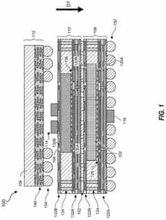
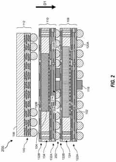
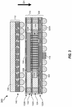
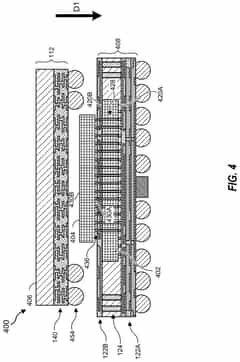
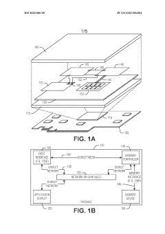
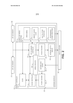
3D chiplet integration using fan-out wafer-level packaging
PatentPendingUS20240274587A1
Innovation
- The use of fan-out wafer-level packaging and three-dimensional packaging techniques for combining semiconductor chips and embedded memory in configurations such as face-to-back, back-to-back, and face-to-face orientations, enabling direct connections between chiplets and reducing assembly package sizes and manufacturing complexity.
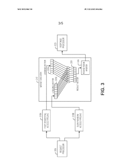
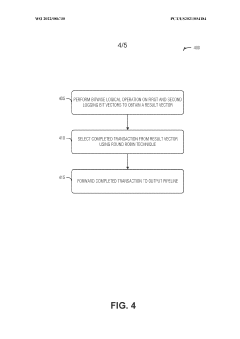
Asynchronous pipeline merging using long vector arbitration
PatentWO2022086730A1
Innovation
- The implementation of long vector arbitration using bitwise operations to represent transactions across parallel paths, allowing for asynchronous and independent completion logging, and a round-robin arbiter to ensure fair handling of completed transactions, thereby maintaining pipeline integrity and throughput.
Regulatory Framework Impact Assessment
The evolving landscape of chiplet integration necessitates a comprehensive assessment of its impact on existing regulatory frameworks. Current semiconductor regulations were primarily designed for monolithic chip architectures, creating significant gaps when applied to multi-die chiplet systems. These regulatory disparities manifest across multiple domains including safety certification, electromagnetic compatibility standards, and international trade regulations.
Regulatory bodies worldwide are struggling to adapt their frameworks to accommodate the distributed nature of chiplet designs. The European Union's Electronic Components and Systems Strategic Research Agenda has recently acknowledged the need for updated standards specifically addressing heterogeneous integration technologies. Similarly, the U.S. Department of Commerce has initiated a review of export control regulations to address the unique challenges posed by chiplet-based systems crossing international borders.
Testing and certification protocols face particular challenges as traditional boundary scan methodologies prove insufficient for inter-chiplet connections. The IEEE P2851 working group has begun developing new standards for chiplet-to-chiplet interfaces, but full regulatory adoption remains years away. This regulatory lag creates uncertainty for manufacturers and potentially slows market adoption of advanced chiplet solutions.
Security and data protection regulations present another critical dimension requiring assessment. The distributed processing nature of chiplet systems creates novel attack vectors not addressed in current cybersecurity frameworks. The fragmentation of processing across multiple dies from potentially different vendors introduces complex questions of security responsibility and liability that remain unresolved in current regulatory structures.
Energy efficiency standards also require recalibration for chiplet architectures. While chiplets often deliver superior performance-per-watt metrics compared to monolithic designs, existing energy certification programs lack appropriate measurement methodologies for heterogeneous systems. The EU's Ecodesign Directive and Energy Star program are currently evaluating modifications to accommodate these architectural differences.
Intellectual property protection frameworks face particular strain from chiplet integration. The collaborative nature of chiplet ecosystems, where multiple vendors contribute different dies to a single package, creates complex IP ownership scenarios not well-addressed by current patent and trade secret laws. Industry consortia like CHIPS Alliance are developing open interface standards, but regulatory frameworks for IP protection in chiplet contexts remain underdeveloped.
Standardization Efforts in Chiplet Industry
The standardization landscape for chiplet technology is rapidly evolving as industry stakeholders recognize the critical need for common frameworks to enable multi-vendor interoperability. The Universal Chiplet Interconnect Express (UCIe) consortium, formed in 2022, represents a significant milestone in these efforts, bringing together major players including Intel, AMD, Arm, TSMC, and Samsung. UCIe aims to establish an open industry standard for die-to-die interconnects, focusing on physical layer, protocol stack, and software specifications that enable chiplets from different vendors to work seamlessly together.
Parallel to UCIe, the Open Compute Project (OCP) has developed the Bunch of Wires (BoW) specification, which offers a simpler, more cost-effective approach to chiplet interconnection. This standard targets applications where ultimate performance may be less critical than implementation simplicity and cost efficiency, providing an alternative path for chiplet integration.
JEDEC, a long-established standards organization in the semiconductor industry, has also entered the chiplet standardization arena with its JC70.1 committee focusing on computational RAM for heterogeneous processing. Their work complements other standardization efforts by addressing memory integration aspects of chiplet-based systems.
The IEEE, meanwhile, has launched the P2851 standard initiative for heterogeneous integration interconnect testing, addressing the critical need for standardized testing methodologies in multi-die systems. This standard aims to ensure reliability and performance consistency across different chiplet implementations.
Industry consortia like the Heterogeneous Integration Roadmap (HIR) team are working to create technology roadmaps that guide future chiplet development, while the CHIPS Alliance focuses on open-source hardware designs and tools that support chiplet-based architectures. These collaborative efforts are essential for establishing a comprehensive ecosystem that supports chiplet innovation.
The standardization landscape also includes regional initiatives, with the European Chips Act and similar programs in Asia promoting local standards development that aligns with global frameworks while addressing specific regional requirements. These efforts reflect the strategic importance of chiplet technology in semiconductor sovereignty initiatives worldwide.
Despite significant progress, challenges remain in harmonizing competing standards and addressing gaps in areas such as thermal management, security protocols, and software abstraction layers. The industry continues to work toward a more unified approach that balances innovation with interoperability, recognizing that robust standards are essential for chiplet technology to reach its full potential in transforming semiconductor design and manufacturing.
Unlock deeper insights with Patsnap Eureka Quick Research — get a full tech report to explore trends and direct your research. Try now!
Generate Your Research Report Instantly with AI Agent
Supercharge your innovation with Patsnap Eureka AI Agent Platform!