

Chiplet Integration: Enhancing Patented Electronics Technologies
OCT 15, 20259 MIN READ
Generate Your Research Report Instantly with AI Agent
PatSnap Eureka helps you evaluate technical feasibility & market potential.
Chiplet Technology Evolution and Integration Goals
The evolution of chiplet technology represents a paradigm shift in semiconductor design and manufacturing, moving away from monolithic system-on-chip (SoC) architectures toward modular, disaggregated approaches. This transition began in the early 2010s as semiconductor manufacturers encountered increasing challenges with traditional Moore's Law scaling. The physical limitations of silicon, rising manufacturing costs, and diminishing returns on transistor shrinkage necessitated innovative solutions to continue advancing computational capabilities.
Chiplets emerged as a revolutionary concept allowing complex systems to be built from smaller, specialized silicon dies manufactured using optimal process nodes for each function. This approach enables the integration of heterogeneous technologies—logic, memory, analog, RF components—each fabricated using the most suitable manufacturing process, then interconnected on a common substrate or interposer.
The historical trajectory shows three distinct phases: early experimentation (2010-2015), commercial adoption (2016-2020), and the current acceleration phase (2021-present). Early implementations focused primarily on multi-chip modules with relatively simple interconnects. The technology has since evolved toward sophisticated 2.5D and 3D integration schemes with advanced packaging technologies like silicon interposers, through-silicon vias (TSVs), and direct copper-to-copper bonding.
Current technical goals for chiplet integration center on standardization of interfaces, improved thermal management, and enhanced yield optimization. The Universal Chiplet Interconnect Express (UCIe) consortium, formed in 2022, represents a significant industry effort to establish common protocols for chiplet-to-chiplet communication, potentially enabling a true chiplet ecosystem with interoperable components from multiple vendors.
Power efficiency remains a critical objective, with research focused on minimizing the energy cost of data movement between chiplets. This includes development of advanced interconnect technologies with reduced parasitic capacitance and resistance, as well as optimized signaling protocols that minimize active power consumption.
Manufacturing scalability constitutes another key goal, with efforts directed toward reducing the complexity and cost of advanced packaging processes. This includes innovations in handling, alignment, and bonding technologies to enable high-volume production of chiplet-based systems with yields comparable to traditional monolithic designs.
The ultimate vision for chiplet technology is to enable a modular, mix-and-match approach to system design, where specialized functional blocks can be rapidly integrated to create customized solutions for specific applications, dramatically reducing development time and cost while maximizing performance and energy efficiency.
Market Demand Analysis for Chiplet-Based Electronics
The chiplet integration market is experiencing unprecedented growth, driven by the increasing demand for high-performance computing solutions across various industries. As traditional monolithic chip designs reach their physical and economic limits, chiplet-based architectures have emerged as a viable alternative, offering enhanced performance, improved yield, and cost efficiency. Market research indicates that the global chiplet market is projected to grow at a compound annual growth rate of 40% from 2023 to 2028, reaching substantial market valuation by the end of the forecast period.
The primary demand drivers for chiplet technology stem from data centers and cloud service providers seeking more efficient computing solutions to handle exponentially growing workloads. These entities require processors with higher transistor counts and specialized accelerators that can be economically manufactured and easily upgraded. Chiplet architecture addresses these needs by allowing the integration of heterogeneous dies manufactured using different process nodes, optimizing both performance and cost.
Consumer electronics represents another significant market segment, with smartphone manufacturers exploring chiplet integration to overcome space constraints while enhancing device capabilities. The automotive industry is also rapidly adopting advanced semiconductor solutions for autonomous driving systems, creating additional demand for chiplet-based electronics that offer high reliability and performance in compact form factors.
Geographically, North America currently leads the chiplet market due to the presence of major semiconductor companies and technology giants. However, Asia-Pacific is expected to witness the fastest growth, supported by expanding manufacturing capabilities in Taiwan, South Korea, and China, along with increasing investments in semiconductor research and development.
From a supply chain perspective, the market shows interesting dynamics. The complexity of chiplet integration requires advanced packaging technologies, creating new opportunities for outsourced semiconductor assembly and test (OSAT) providers. This has led to strategic partnerships between traditional integrated device manufacturers (IDMs), fabless companies, and packaging specialists to develop comprehensive chiplet ecosystems.
Industry surveys reveal that over 70% of semiconductor professionals believe chiplet technology will become the dominant architecture for high-performance computing applications within the next five years. This sentiment is reflected in the increasing number of patent filings related to chiplet integration technologies, which have grown by approximately 35% annually since 2020.
The market is also witnessing the emergence of standardization efforts, such as the Universal Chiplet Interconnect Express (UCIe) consortium, which aims to establish industry-wide interfaces for chiplet integration. These initiatives are expected to accelerate market adoption by enabling interoperability between chiplets from different vendors, potentially transforming the semiconductor industry's business model toward more specialized and collaborative approaches.
Current Challenges in Chiplet Integration Technologies
Despite significant advancements in chiplet integration technologies, several critical challenges continue to impede broader implementation and optimization. The most pressing issue remains the interconnect bottleneck, where the communication interfaces between chiplets still struggle with bandwidth limitations, signal integrity degradation, and power efficiency concerns. Current die-to-die interconnect solutions often face trade-offs between performance, power consumption, and manufacturing complexity that have not been fully resolved.
Thermal management presents another substantial hurdle as heterogeneous integration brings together components with different thermal characteristics and power densities. The resulting hotspots and thermal gradients can significantly impact system reliability and performance, while conventional cooling solutions prove inadequate for these complex three-dimensional structures.
Testing and validation methodologies have not kept pace with chiplet advancement. Known-good-die testing remains challenging, particularly when chiplets originate from different vendors with varying test protocols. The industry lacks standardized testing frameworks that can effectively evaluate integrated chiplet systems while maintaining economic viability in production environments.
Manufacturing yield and cost considerations continue to challenge widespread adoption. While chiplet approaches theoretically improve yield by using smaller dies, the complexity of integration processes introduces new failure modes. Advanced packaging technologies required for high-performance chiplet integration, such as silicon interposers and bridge technologies, remain expensive and technically demanding.
Design tool ecosystems present significant limitations, as existing EDA platforms were primarily developed for monolithic chip design rather than multi-chiplet systems. The tools struggle with cross-domain optimization spanning electrical, thermal, and mechanical considerations across chiplet boundaries. This gap hampers designers' ability to fully exploit chiplet architecture advantages.
Standardization efforts, while progressing through initiatives like UCIe (Universal Chiplet Interconnect Express), remain fragmented. The industry continues to grapple with competing interface protocols, physical specifications, and business models for chiplet exchange. This fragmentation creates market uncertainty and slows adoption across the semiconductor ecosystem.
Intellectual property protection and business model evolution represent emerging challenges as chiplet marketplaces develop. Questions regarding chiplet compatibility verification, responsibility for system-level performance, and fair value distribution across the supply chain remain largely unresolved, creating barriers to the formation of robust chiplet supply chains.
Current Patented Chiplet Integration Solutions
01 Advanced Interconnect Technologies for Chiplet Integration
Various interconnect technologies are being developed to enhance chiplet integration, including advanced packaging methods, high-density interconnects, and novel bonding techniques. These technologies aim to improve the communication bandwidth between chiplets while reducing latency and power consumption. Innovations in this area focus on creating seamless connections between different chiplets to enable high-performance computing systems with modular architectures.- Advanced Interconnect Technologies for Chiplet Integration: Various interconnect technologies are being developed to enhance chiplet integration, including advanced packaging methods that allow for high-density connections between chiplets. These technologies focus on improving signal integrity, reducing latency, and increasing bandwidth between chiplets. Innovations in this area include through-silicon vias (TSVs), microbumps, and hybrid bonding techniques that enable more efficient communication between chiplets in a multi-die system.
- Thermal Management Solutions for Chiplet Architectures: Effective thermal management is crucial for chiplet integration as heat dissipation becomes more challenging with increased component density. Innovations in this area include advanced cooling solutions, thermal interface materials, and heat spreading techniques specifically designed for chiplet-based systems. These solutions help maintain optimal operating temperatures across multiple chiplets, preventing thermal throttling and ensuring reliable performance of the integrated system.
- Power Delivery Network Optimization for Chiplet Systems: Power delivery network (PDN) optimization is essential for chiplet integration to ensure stable and efficient power distribution across multiple dies. Innovations focus on reducing power loss, minimizing voltage droop, and improving power integrity in chiplet-based systems. Advanced PDN designs incorporate novel power delivery architectures, integrated voltage regulators, and optimized power routing strategies to meet the unique power requirements of heterogeneous chiplet integration.
- Heterogeneous Integration and Die-to-Die Communication Protocols: Heterogeneous integration enables combining chiplets manufactured using different process technologies into a single package. This approach requires specialized die-to-die communication protocols and interfaces to ensure seamless operation between diverse chiplets. Innovations in this area include standardized communication interfaces, high-speed serializer/deserializer (SerDes) circuits, and optimized signaling techniques that facilitate efficient data transfer between chiplets with different functionalities and manufacturing processes.
- Design Automation and Testing Methodologies for Chiplet Systems: Design automation tools and testing methodologies specifically tailored for chiplet-based systems are being developed to address the unique challenges of multi-die integration. These innovations include advanced electronic design automation (EDA) tools for chiplet-aware design, pre-silicon validation techniques, and post-assembly testing methods. Such tools and methodologies help optimize chiplet placement, routing, and verification, while ensuring manufacturability and reliability of the integrated system.
02 Thermal Management Solutions for Chiplet Designs
Effective thermal management is crucial for chiplet integration as it directly impacts system performance and reliability. Various approaches include integrated heat spreaders, advanced thermal interface materials, and active cooling solutions specifically designed for multi-chiplet packages. These solutions help dissipate heat efficiently across the entire package, preventing hotspots and thermal throttling while enabling higher performance and improved reliability in densely packed chiplet architectures.Expand Specific Solutions03 Power Delivery Network Optimization for Chiplet Systems
Optimizing power delivery networks is essential for chiplet-based systems to ensure stable and efficient power distribution across multiple integrated dies. Innovations include advanced power delivery architectures, integrated voltage regulators, and novel power distribution techniques that minimize power loss and voltage droop. These optimizations help maintain performance consistency across chiplets while reducing overall power consumption and improving energy efficiency in complex multi-die packages.Expand Specific Solutions04 Heterogeneous Integration of Chiplets
Heterogeneous integration enables combining chiplets manufactured using different process technologies or having different functionalities into a single package. This approach allows for optimizing each component separately while achieving overall system performance improvements. Techniques include die-to-die interfaces designed for compatibility between different process nodes, bridge chips that facilitate communication between heterogeneous chiplets, and specialized packaging solutions that accommodate different chiplet types and sizes.Expand Specific Solutions05 Testing and Yield Improvement for Chiplet-Based Systems
Testing methodologies and yield improvement techniques specifically designed for chiplet-based systems are crucial for commercial viability. These include pre-integration testing protocols, known-good-die selection strategies, and built-in self-test capabilities for individual chiplets and their interconnections. Advanced testing approaches help identify defects early in the manufacturing process, improving overall yield and reducing costs while ensuring reliability of the final integrated system.Expand Specific Solutions
Key Industry Players in Chiplet Ecosystem
Chiplet integration is currently in a growth phase within the semiconductor industry, with the market expected to expand significantly due to increasing demand for advanced computing solutions. The technology has reached moderate maturity, with key players like TSMC, Intel, AMD, and Samsung leading development efforts. These companies are leveraging chiplet architectures to overcome monolithic chip scaling limitations while improving performance and reducing costs. Micron and SK hynix are advancing memory integration within chiplet designs, while Huawei and IBM are developing innovative packaging technologies. The ecosystem is expanding with specialized players like Renesas and Infineon contributing domain-specific solutions, creating a competitive landscape that balances collaboration and proprietary development as the technology continues to evolve toward standardization.
Taiwan Semiconductor Manufacturing Co., Ltd.
Technical Solution: TSMC's chiplet integration strategy centers around their advanced packaging technologies, particularly their Integrated Fan-Out (InFO) and System on Integrated Chips (SoIC) platforms. Their CoWoS (Chip on Wafer on Substrate) technology provides high-density interconnects between chiplets using silicon interposers, enabling thousands of connections between dies. TSMC's 3DFabric architecture combines frontend and backend technologies to create a comprehensive 3D IC solution platform. Their SoIC technology uses wafer-on-wafer and chip-on-wafer bonding with microbump-free hybrid bonding, achieving sub-2μm interconnect pitch between chiplets. This enables ultra-high-density die-to-die connections with significantly lower parasitic capacitance and resistance compared to traditional microbump approaches. TSMC has demonstrated their technology in collaboration with customers like AMD and Apple, achieving interconnect pitches below 9μm in production systems. Their latest developments include their LIPINCON (Low-voltage-In-Package-INterCONnect) technology, which reduces the energy consumption of die-to-die links by approximately 96% compared to conventional SerDes approaches.
Strengths: TSMC's position as the leading semiconductor foundry gives them unparalleled process technology advantages and customer relationships. Their hybrid bonding technology achieves industry-leading interconnect density. Weaknesses: As a foundry, TSMC depends on customers' chiplet designs and must support multiple interconnect standards rather than driving a single proprietary solution.
Advanced Micro Devices, Inc.
Technical Solution: AMD pioneered commercial chiplet implementation with their Infinity Fabric interconnect technology, which enables high-bandwidth, low-latency communication between multiple dies within a package. Their approach divides processor designs into smaller chiplets manufactured on optimized process nodes - compute dies on advanced nodes and I/O dies on mature nodes. This strategy is exemplified in their EPYC server processors and Ryzen desktop processors, where multiple Core Complex Dies (CCDs) connect to a central I/O die. AMD's 3D V-Cache technology further extends their chiplet capabilities by vertically stacking cache memory directly on top of processor dies using through-silicon vias (TSVs), significantly increasing cache capacity without expanding the processor's footprint. Their latest implementations use their 4th generation Infinity Architecture with improved coherency and reduced latency between chiplets, supporting both organic and silicon interposer substrates for different performance tiers.
Strengths: AMD's chiplet approach enables cost-effective scaling of processor cores while maintaining high yields. Their design allows mixing of process nodes to optimize performance/cost. Weaknesses: Inter-chiplet communication introduces some latency penalties compared to monolithic designs, and their implementation has historically been more limited to homogeneous compute tiles rather than highly heterogeneous integration.
Core IP Analysis for Chiplet Interconnect Technologies
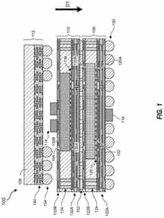
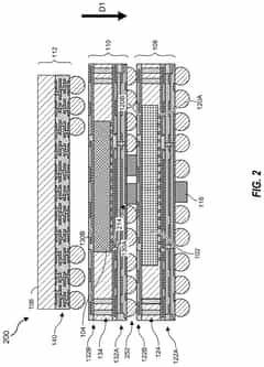
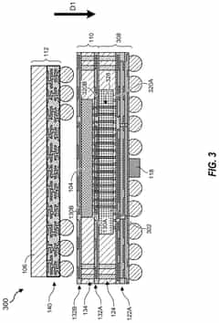
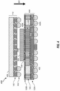
3D chiplet integration using fan-out wafer-level packaging
PatentPendingUS20240274587A1
Innovation
- The use of fan-out wafer-level packaging and three-dimensional packaging techniques for combining semiconductor chips and embedded memory in configurations such as face-to-back, back-to-back, and face-to-face orientations, enabling direct connections between chiplets and reducing assembly package sizes and manufacturing complexity.
Edge interface placements to enable chiplet rotation into multi-chiplet cluster
PatentWO2022119635A2
Innovation
- The placement of I/O pads at the edges of chiplets in a symmetrical arrangement relative to the centerline, allowing for rotation to achieve proper alignment and close-coupled interconnects, thereby facilitating dense packaging and minimizing the system footprint.
Standardization Efforts in Chiplet Interfaces
The standardization of chiplet interfaces represents a critical evolutionary step in the semiconductor industry's transition toward disaggregated chip designs. Industry consortia such as the Universal Chiplet Interconnect Express (UCIe) have emerged as pivotal forces in establishing common protocols for die-to-die communication. UCIe's founding members, including Intel, AMD, Arm, TSMC, and Samsung Electronics, have collaboratively developed specifications covering both the physical layer and protocol stack to ensure interoperability across different vendors' chiplets.
Parallel to UCIe, other significant standardization initiatives include JEDEC's Chiplet PHY Express (CPX) and the Open Compute Project's Bunch of Wires (BoW) specification. These competing standards address varying technical requirements and market segments, with CPX focusing on memory-centric applications while BoW targets cost-sensitive implementations with moderate bandwidth requirements.
The IEEE has also entered the standardization landscape with the P3172 working group, which aims to establish testing and verification methodologies specifically for chiplet-based systems. This effort addresses the critical need for consistent quality assurance protocols in multi-vendor chiplet ecosystems.
Standardization efforts extend beyond electrical interfaces to encompass thermal management, mechanical form factors, and testing methodologies. The Advanced Semiconductor Test Interface Specification (ASTI) consortium has been developing standards for chiplet testing that enable efficient known-good-die verification before integration into multi-chiplet packages.
Patent analysis reveals increasing activity around standardized interfaces, with major semiconductor companies filing strategic patents that both contribute to and leverage these emerging standards. Companies are carefully positioning their intellectual property portfolios to influence standard development while ensuring freedom to operate within the standardized ecosystem.
The economic implications of successful chiplet interface standardization are substantial, potentially reducing design costs by 20-30% through reusable IP blocks and enabling a more diverse supplier ecosystem. Market research indicates that standardized chiplets could accelerate time-to-market for new products by up to 40% compared to traditional monolithic approaches.
Despite progress, challenges remain in achieving full interoperability across different process nodes and packaging technologies. Current standards primarily address electrical connectivity, while more comprehensive specifications for power delivery, thermal management, and security features are still evolving. The industry continues to balance the need for standardization against competitive differentiation in this rapidly developing technological domain.
Supply Chain Resilience Through Chiplet Design
The chiplet architecture represents a paradigm shift in semiconductor manufacturing, offering unprecedented supply chain resilience in an era of geopolitical tensions and market volatility. By disaggregating monolithic system-on-chip designs into smaller functional blocks, organizations can diversify their manufacturing partnerships across multiple geographical regions, effectively mitigating regional supply disruptions.
This approach enables companies to strategically source different chiplets from various foundries based on their specialized manufacturing capabilities, creating redundancy in the supply network. When one region experiences production constraints due to natural disasters, political sanctions, or pandemic-related shutdowns, production can be rapidly shifted to alternative suppliers with minimal redesign efforts.
The modular nature of chiplet design also accelerates time-to-market by allowing parallel development tracks. Companies can update specific functional blocks without redesigning the entire system, resulting in more agile product development cycles that can quickly respond to supply chain disruptions or component shortages.
From a manufacturing perspective, chiplet designs typically achieve higher yields compared to monolithic approaches. Smaller die sizes inherently have better yield rates, reducing waste and improving production efficiency. This yield advantage becomes particularly valuable during supply constraints when maximizing output from limited manufacturing capacity is essential.
The standardization efforts around chiplet interfaces, such as UCIe (Universal Chiplet Interconnect Express), are further enhancing supply chain flexibility. As these standards mature, the industry moves closer to a true "chiplet marketplace" where functional blocks become interchangeable commodities that can be sourced from multiple vendors, dramatically reducing single-source dependencies.
Additionally, chiplet architecture enables more efficient use of leading-edge process nodes only where absolutely necessary, while utilizing mature nodes for less performance-critical components. This "right-node-for-right-function" approach reduces reliance on the most constrained manufacturing capabilities, which are typically concentrated in geopolitically sensitive regions.
For organizations implementing patented electronics technologies, chiplet integration offers a strategic advantage in protecting intellectual property while maintaining manufacturing flexibility. Critical proprietary circuits can be isolated in specific chiplets manufactured under tightly controlled conditions, while standard components can be sourced through broader supply channels.
Unlock deeper insights with PatSnap Eureka Quick Research — get a full tech report to explore trends and direct your research. Try now!
Generate Your Research Report Instantly with AI Agent
Supercharge your innovation with PatSnap Eureka AI Agent Platform!