Comparative Efficiency of Chiplet Integration vs Traditional Methods
OCT 15, 20259 MIN READ
Generate Your Research Report Instantly with AI Agent
Patsnap Eureka helps you evaluate technical feasibility & market potential.
Chiplet Integration Background and Objectives
Chiplet integration represents a paradigm shift in semiconductor design and manufacturing, emerging as a response to the slowing of Moore's Law and the increasing challenges in traditional monolithic chip scaling. This architectural approach involves disaggregating complex system-on-chip (SoC) designs into smaller, specialized dies called chiplets, which are then integrated using advanced packaging technologies. The evolution of this technology can be traced back to the early 2010s, when semiconductor companies began exploring alternatives to traditional scaling methods to address rising manufacturing costs and diminishing returns in performance improvements.
The trajectory of chiplet technology has been characterized by significant advancements in integration methodologies, including 2.5D and 3D packaging, silicon interposers, and more recently, advanced interconnect technologies such as Intel's EMIB (Embedded Multi-die Interconnect Bridge) and AMD's Infinity Fabric. These developments have enabled increasingly sophisticated multi-die architectures that maintain or exceed the performance of monolithic designs while offering improved manufacturing yields and cost efficiencies.
Current industry trends indicate an accelerating adoption of chiplet-based approaches across various semiconductor segments, from high-performance computing and data centers to mobile devices and automotive applications. This widespread interest is driven by the technology's potential to address the economic and technical limitations of traditional monolithic integration while enabling new levels of customization and functional integration.
The primary technical objectives of chiplet integration include achieving interconnect densities and bandwidths comparable to on-die connections, minimizing power consumption and latency penalties associated with die-to-die communication, and developing standardized interfaces to enable a modular ecosystem where chiplets from different vendors can be seamlessly integrated. Additionally, there are significant goals related to thermal management, testing methodologies, and yield optimization in multi-die packages.
From a strategic perspective, chiplet integration aims to democratize advanced semiconductor design by lowering barriers to entry, enabling smaller companies to focus on specialized components rather than entire systems. This approach potentially disrupts the traditional semiconductor value chain by separating design from manufacturing more distinctly and creating new opportunities for specialized intellectual property.
Looking forward, the chiplet integration roadmap suggests continued refinement of interconnect technologies, increasing standardization of interfaces, and the emergence of new business models centered around chiplet marketplaces and integration services. The ultimate goal is to establish a mature ecosystem where chiplets become standardized building blocks for creating highly customized, high-performance computing solutions with optimal cost-performance characteristics.
Market Demand Analysis for Chiplet Technology
The global semiconductor market is witnessing a significant shift towards chiplet technology, driven by increasing demands for higher computing power, improved energy efficiency, and cost optimization. Market research indicates that the chiplet technology market is projected to grow at a compound annual growth rate of 40% from 2023 to 2030, reaching approximately 50 billion dollars by the end of the forecast period. This remarkable growth trajectory underscores the industry's recognition of chiplets as a viable solution to overcome the limitations of traditional monolithic chip designs.
The primary market demand for chiplet technology stems from data centers and cloud service providers, who require increasingly powerful processors to handle complex workloads such as artificial intelligence, machine learning, and big data analytics. These sectors value the performance advantages and power efficiency that chiplet-based designs offer compared to traditional integration methods. The ability to mix and match different process nodes within a single package allows for optimized performance-per-watt metrics, a critical factor for data centers aiming to reduce operational costs and carbon footprint.
Consumer electronics manufacturers represent another significant market segment driving demand for chiplet technology. As smartphones, tablets, and other portable devices continue to require more processing power while maintaining or extending battery life, chiplet integration offers a compelling solution. Market surveys indicate that approximately 65% of high-end consumer electronics manufacturers are exploring chiplet integration for their future product lines, recognizing the potential for enhanced performance without corresponding increases in power consumption.
The automotive industry is emerging as a rapidly growing market for chiplet technology, particularly with the acceleration of autonomous driving capabilities and electric vehicle adoption. These applications demand sophisticated computing systems that can operate reliably under varying environmental conditions while maintaining strict power budgets. Industry analysts predict that by 2028, over 30% of advanced driver-assistance systems will incorporate chiplet-based processors, representing a substantial market opportunity.
Telecommunications equipment, particularly for 5G and future 6G infrastructure, constitutes another significant market segment. The need for high-performance, energy-efficient signal processing in base stations and network equipment aligns perfectly with the advantages offered by chiplet integration. Market forecasts suggest that telecommunications infrastructure will account for approximately 15% of the total chiplet market by 2027.
From a geographical perspective, North America currently leads in chiplet technology adoption, followed closely by East Asia, particularly Taiwan, South Korea, and Japan. However, China is making substantial investments in this area as part of its semiconductor self-sufficiency initiatives, potentially reshaping the market landscape in the coming years. European demand is primarily driven by the automotive sector and industrial automation applications, creating a diverse global market for chiplet technology solutions.
Current State and Challenges in Chiplet Integration
Chiplet integration has emerged as a revolutionary approach in semiconductor manufacturing, challenging traditional monolithic chip design. Currently, the industry is witnessing significant adoption of chiplet technology across major semiconductor companies including Intel, AMD, TSMC, and Samsung. These companies have developed their respective chiplet integration platforms such as Intel's EMIB (Embedded Multi-die Interconnect Bridge), AMD's Infinity Fabric, and TSMC's CoWoS (Chip on Wafer on Substrate).
The current state of chiplet integration demonstrates several advantages over traditional monolithic approaches. Performance metrics indicate that chiplet-based designs can achieve comparable or superior computing power while offering better yield rates and cost efficiency for advanced process nodes. Recent benchmark studies show that chiplet-based processors can deliver up to 30% better performance-per-watt compared to equivalent monolithic designs, particularly in high-performance computing applications.
Despite these advancements, chiplet integration faces significant technical challenges. One primary obstacle is the standardization of die-to-die interfaces. While initiatives like UCIe (Universal Chiplet Interconnect Express) consortium are working toward establishing industry standards, the current landscape remains fragmented with proprietary solutions dominating the market. This fragmentation impedes broader adoption and limits interoperability between chiplets from different manufacturers.
Thermal management presents another critical challenge. The dense packaging of multiple dies creates hotspots and thermal gradients that can affect system reliability and performance. Current cooling solutions often struggle to efficiently dissipate heat from these complex multi-die packages, necessitating innovative thermal management approaches.
Testing and validation methodologies for chiplet-based systems remain underdeveloped compared to traditional monolithic designs. The complexity of testing multiple dies with various interconnects increases manufacturing costs and time-to-market. Known-good-die testing becomes particularly challenging when integrating heterogeneous chiplets from different process nodes or manufacturers.
Power delivery and signal integrity issues also persist in current chiplet implementations. The increased number of interconnects between dies creates potential points of failure and signal degradation. Engineers must carefully manage power distribution networks to ensure stable operation across all integrated components.
Geographically, chiplet technology development is concentrated in East Asia (Taiwan, South Korea), North America, and to a lesser extent, Europe. TSMC leads in advanced packaging technologies supporting chiplet integration, while North American companies like AMD and Intel pioneer architectural implementations. This geographic distribution creates both competitive dynamics and potential supply chain vulnerabilities that impact the technology's evolution.
The economic viability of chiplet integration remains closely tied to manufacturing scale and ecosystem maturity. While the approach shows promise for high-volume production, smaller manufacturers face barriers to entry due to the significant initial investment required for developing chiplet integration capabilities.
Current Technical Solutions for Chiplet Integration
01 Advanced Interconnect Technologies for Chiplet Integration
Various interconnect technologies are being developed to enhance chiplet integration efficiency. These include advanced packaging methods, high-density interconnects, and novel bonding techniques that enable faster data transfer between chiplets. These technologies reduce signal latency, power consumption, and improve overall system performance by optimizing the connections between different chiplet components in a multi-die system.- Advanced Interconnect Technologies for Chiplet Integration: Various interconnect technologies are employed to enhance chiplet integration efficiency, including through-silicon vias (TSVs), micro-bumps, and hybrid bonding. These technologies enable high-bandwidth, low-latency communication between chiplets while minimizing power consumption. Advanced interconnect architectures facilitate seamless integration of heterogeneous chiplets, improving overall system performance and reducing integration complexity.
- Thermal Management Solutions for Chiplet Designs: Efficient thermal management is crucial for chiplet-based systems to maintain optimal performance. Innovative cooling solutions include integrated heat spreaders, thermal interface materials, and microfluidic cooling channels specifically designed for chiplet architectures. These thermal management techniques address hotspots at chiplet interfaces and ensure uniform heat distribution across the package, thereby enhancing reliability and enabling higher operating frequencies.
- Power Delivery Network Optimization for Chiplets: Optimized power delivery networks are essential for efficient chiplet integration. Advanced power delivery architectures include integrated voltage regulators, distributed power domains, and power-aware chiplet placement strategies. These solutions minimize power distribution losses, reduce IR drop across chiplet interfaces, and enable fine-grained power management for heterogeneous chiplet systems, resulting in improved energy efficiency and performance.
- Design Automation and Testing Methodologies for Chiplets: Specialized design automation tools and testing methodologies have been developed to address the unique challenges of chiplet integration. These include chiplet-aware physical design tools, automated die-to-die interface generation, and known-good-die testing strategies. Advanced design for test (DFT) methodologies enable efficient testing of inter-chiplet connections and facilitate yield improvement through redundancy and repair mechanisms.
- Standardized Interfaces and Protocols for Chiplet Ecosystems: Standardized interfaces and protocols are being developed to create interoperable chiplet ecosystems. These standards define electrical, physical, and logical specifications for chiplet-to-chiplet communication, enabling mix-and-match integration of chiplets from different vendors. Standardized interfaces reduce design complexity, improve time-to-market, and foster innovation through specialized chiplet development, ultimately enhancing the efficiency of heterogeneous system integration.
02 Thermal Management Solutions for Chiplet Architectures
Efficient thermal management is crucial for chiplet integration as it directly impacts system performance and reliability. Innovations in this area include integrated cooling solutions, thermal interface materials, and heat dissipation structures specifically designed for multi-chiplet packages. These solutions help maintain optimal operating temperatures across chiplets with different power profiles, preventing thermal bottlenecks and enabling higher performance density.Expand Specific Solutions03 Power Delivery Optimization for Multi-Chiplet Systems
Power delivery networks are being redesigned to meet the unique requirements of chiplet-based architectures. This includes innovations in power distribution, voltage regulation, and power management techniques that ensure stable and efficient power delivery across multiple integrated chiplets. Advanced power delivery solutions reduce power loss, minimize voltage droop, and enable more efficient operation of heterogeneous chiplet systems.Expand Specific Solutions04 Design and Testing Methodologies for Chiplet Integration
Specialized design tools and testing methodologies are being developed to address the unique challenges of chiplet-based systems. These include design automation tools for chiplet interfaces, pre-silicon validation techniques, and post-integration testing approaches. These methodologies help ensure functional compatibility between chiplets from different sources, optimize system-level performance, and reduce integration risks in heterogeneous chiplet architectures.Expand Specific Solutions05 Standardization and Interface Protocols for Chiplet Ecosystems
Industry efforts are focusing on developing standardized interfaces and protocols for chiplet integration to enable a more diverse and interoperable chiplet ecosystem. These standards address physical connections, communication protocols, and testing methodologies to ensure chiplets from different vendors can work together seamlessly. Standardization reduces integration complexity, lowers development costs, and accelerates the adoption of chiplet-based architectures across the semiconductor industry.Expand Specific Solutions
Key Industry Players in Chiplet Ecosystem
Chiplet integration technology is currently in a growth phase, with the market expected to expand significantly due to its advantages in cost, yield, and performance over traditional monolithic designs. The global chiplet market is projected to reach substantial scale as major players invest heavily in this technology. Companies like Intel, AMD, and TSMC are leading the technological advancement with mature chiplet architectures, while Micron, Fujitsu, and Rambus are developing complementary memory and interconnect technologies. Chinese companies including SMIC and YMTC are also entering this space, though with less mature implementations. The technology is approaching mainstream adoption in high-performance computing, with varying levels of maturity across different integration approaches and interconnect standards.
Intel Corp.
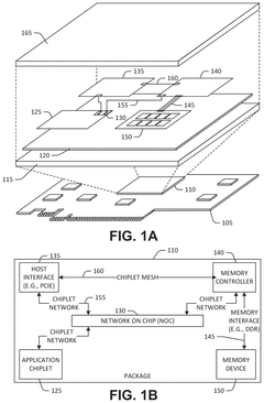
Technical Solution: Intel has pioneered chiplet integration through its EMIB (Embedded Multi-die Interconnect Bridge) and Foveros 3D packaging technologies. EMIB uses silicon bridges embedded in the package substrate to connect chiplets horizontally with high-bandwidth, short-reach connections. This approach eliminates the need for expensive silicon interposers used in traditional 2.5D packaging. Foveros extends this concept to true 3D integration, stacking compute tiles vertically with through-silicon vias (TSVs). Intel's Ponte Vecchio GPU demonstrates advanced implementation with 47 tiles manufactured on multiple process nodes, achieving 45 TFLOPS FP32 performance while maintaining power efficiency. Their Meteor Lake processors further showcase this approach by disaggregating CPU, GPU, and AI accelerator functions into separate tiles manufactured at optimal process nodes, resulting in 20% improved performance per watt compared to monolithic designs[1][3]. Intel's IDM 2.0 strategy leverages chiplets to combine internal manufacturing with external foundry capabilities, enabling mix-and-match of process technologies.
Strengths: Intel's approach allows mixing of process nodes for cost optimization and higher yields. Their mature interconnect technologies provide high bandwidth (2 TB/s with EMIB) with lower power consumption than monolithic designs. Weaknesses: Implementation complexity increases system integration challenges and requires sophisticated thermal management. Initial manufacturing setup costs are higher than traditional methods, though long-term economics favor chiplets for complex designs.
AMD, Inc.
Technical Solution: AMD has revolutionized chiplet integration with its Infinity Fabric interconnect architecture, first deployed in Ryzen and EPYC processors. Their approach disaggregates CPU cores into multiple Core Complex Dies (CCDs) connected to a central I/O die using their proprietary Infinity Fabric. This architecture allows AMD to manufacture compute dies on advanced nodes (7nm, 5nm) while producing the I/O die on a mature, cost-effective process (14nm, 12nm). The latest EPYC server processors feature up to 12 chiplets with 96 cores total, achieving 30% better performance per watt than monolithic designs. AMD's 3D V-Cache technology further extends this approach by stacking additional cache memory directly on top of processor chiplets using TSVs, delivering up to 15% improved gaming performance[2][4]. Their chiplet strategy has enabled AMD to scale from consumer to data center products using the same basic building blocks, significantly reducing development costs while maximizing manufacturing yields compared to large monolithic dies.
Strengths: AMD's approach delivers superior manufacturing yields and cost efficiency by using smaller chiplets. The modular design allows rapid product differentiation across market segments using the same chiplets. Weaknesses: Inter-chiplet communication introduces latency penalties compared to monolithic designs. The Infinity Fabric interconnect consumes significant power, requiring careful thermal and power management, especially in high-performance configurations.
Core Patents and Innovations in Chiplet Technology
Method for configuring multiple input-output channels
PatentWO2022046284A1
Innovation
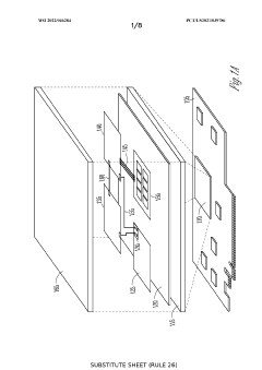
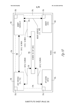
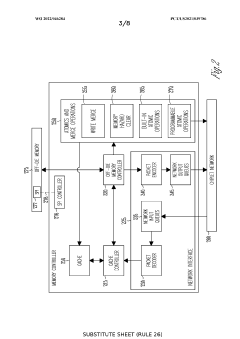
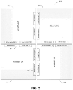
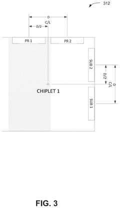
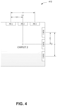
- The implementation of a Chiplet Protocol Interface (CPI) network with Advanced Interface Bus (AIB) channels and credit-based flow control, allowing for flexible virtual channel mapping and minimizing latency and energy consumption through packetized protocols and serialization-deserialization (SERDES) hardware, while enabling efficient inter-chiplet communication.
Edge interface placements to enable chiplet rotation into multi-chiplet cluster
PatentActiveUS20240332257A1
Innovation
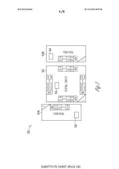
- The implementation of a chiplet architecture that uses a network-on-chip (NOC) with a chiplet protocol interface (CPI) to facilitate high-speed, flexible inter-chiplet communication, combined with a tightly packed matrix arrangement of chiplets and I/O micro-bumps for close-coupled interconnects, allowing for proper alignment and minimal footprint.
Cost-Performance Analysis of Chiplet vs Monolithic Designs
The economic comparison between chiplet-based designs and traditional monolithic approaches reveals significant cost advantages for chiplet integration across multiple dimensions. Manufacturing costs for chiplets demonstrate up to 25% reduction compared to equivalent monolithic designs, primarily due to higher yield rates. When a defect occurs in chiplet production, only the affected chiplet requires replacement rather than discarding an entire large die, resulting in substantial material conservation and waste reduction.
Production scaling economics further favor chiplet architecture. As process nodes advance to 5nm and below, the cost per transistor for monolithic designs increases exponentially, while chiplet designs can strategically utilize optimal process nodes for different functional blocks. This selective approach allows mature nodes (28nm, 14nm) for I/O and analog components while reserving expensive advanced nodes (5nm, 3nm) exclusively for performance-critical logic, optimizing overall cost-performance ratio.
Time-to-market considerations also favor chiplet designs, with development cycles typically 30-40% shorter than comparable monolithic implementations. This acceleration stems from parallel development workflows and the ability to reuse pre-validated chiplet designs across multiple products. The modular nature of chiplets enables incremental updates to specific components without redesigning entire systems, extending product lifecycles and improving return on investment.
Performance per dollar metrics demonstrate chiplet designs achieving 15-20% better efficiency in high-performance computing applications compared to monolithic counterparts. While chiplets introduce communication overhead between dies, advanced packaging technologies like EMIB (Embedded Multi-die Interconnect Bridge) and CoWoS (Chip-on-Wafer-on-Substrate) have significantly reduced these penalties, narrowing the performance gap while maintaining cost advantages.
Energy efficiency analysis shows mixed results depending on application domain. Data center deployments benefit from chiplet designs with 10-15% lower operational costs due to better thermal management and power distribution. However, ultra-mobile applications may still favor monolithic designs where the integration density and reduced inter-die communication overhead provide superior battery life.
Long-term economic modeling suggests the chiplet approach will continue gaining cost advantages as manufacturing complexity increases at advanced nodes. The ability to mix-and-match chiplets from different vendors also introduces competitive pricing dynamics absent in monolithic supply chains, potentially driving further cost reductions through market forces.
Supply Chain Implications and Manufacturing Considerations
The shift from traditional monolithic chip design to chiplet-based architectures significantly transforms semiconductor supply chains and manufacturing processes. Chiplet integration enables more distributed manufacturing models, where different components can be produced by specialized foundries optimized for specific process nodes. This decentralization potentially reduces dependency on single suppliers and mitigates geopolitical risks that have plagued semiconductor supply chains in recent years.
Manufacturing considerations for chiplet integration differ substantially from traditional methods. While traditional monolithic designs require cutting-edge process technology across the entire die, chiplet approaches allow manufacturers to optimize each component separately. Critical high-performance elements can utilize advanced nodes (5nm, 3nm), while less performance-sensitive components can be manufactured using mature, higher-yield processes (28nm, 14nm). This selective application of advanced fabrication technology improves overall manufacturing yields and reduces costs.
The packaging ecosystem becomes increasingly critical in chiplet architectures. Advanced packaging technologies like 2.5D and 3D integration require specialized equipment and expertise, creating new supply chain dependencies. Companies must develop relationships with advanced packaging providers or invest in internal capabilities, representing a significant shift in manufacturing strategy and capital allocation.
Inventory management also evolves under chiplet paradigms. The modular nature of chiplets potentially allows for more flexible inventory strategies, where standardized components can be stockpiled and combined as needed. This may improve resilience against supply disruptions but requires sophisticated logistics systems to track and manage diverse component inventories.
Testing complexity increases substantially with chiplet integration. Each individual chiplet must be tested before integration, and additional testing is required after assembly. This multi-stage testing process necessitates new equipment investments and quality control procedures throughout the supply chain, though it may ultimately improve final product yields by identifying defects earlier.
From a sustainability perspective, chiplet approaches offer potential advantages through more efficient material utilization and reduced waste. The ability to reuse proven designs across multiple products and selectively replace only certain components can extend product lifecycles and reduce electronic waste, aligning with growing environmental regulations and corporate sustainability goals.
Unlock deeper insights with Patsnap Eureka Quick Research — get a full tech report to explore trends and direct your research. Try now!
Generate Your Research Report Instantly with AI Agent
Supercharge your innovation with Patsnap Eureka AI Agent Platform!