Analysis of Directed Energy Deposition in Advanced Electronics
OCT 10, 202510 MIN READ
Generate Your Research Report Instantly with AI Agent
Patsnap Eureka helps you evaluate technical feasibility & market potential.
DED Technology Background and Objectives
Directed Energy Deposition (DED) represents a transformative additive manufacturing technology that has evolved significantly since its inception in the late 1990s. Initially developed for rapid prototyping and repair applications in aerospace and defense sectors, DED has undergone substantial refinement to become a versatile manufacturing process capable of producing complex metal components with exceptional material properties. The technology utilizes focused thermal energy to fuse materials by melting as they are deposited, allowing for precise control over material composition and microstructure.
The evolution of DED technology has been marked by several key advancements, including improved energy source efficiency, enhanced material feeding systems, and sophisticated process monitoring capabilities. These developments have expanded DED's applicability beyond traditional manufacturing sectors into advanced electronics, where miniaturization and performance demands continue to increase exponentially.
In the context of advanced electronics manufacturing, DED offers unique capabilities for creating three-dimensional conductive pathways, embedded sensors, and integrated thermal management systems. The technology's ability to process multiple materials simultaneously presents opportunities for fabricating heterogeneous electronic components with gradient properties and functionality that cannot be achieved through conventional manufacturing methods.
The primary technical objectives for DED in advanced electronics applications include achieving sub-micron resolution deposition, enhancing material compatibility with semiconductor substrates, reducing thermal impact zones, and developing specialized materials formulated specifically for electronic applications. Additionally, there is significant focus on integrating DED processes with existing semiconductor manufacturing workflows to enable hybrid manufacturing approaches.
Current research trajectories are exploring the potential of DED for printing conductive traces directly onto flexible substrates, creating embedded passive components within circuit boards, and developing novel packaging solutions for high-performance computing applications. The technology shows particular promise for next-generation electronics that require complex three-dimensional interconnects and thermal management structures.
Looking forward, the technology roadmap for DED in electronics manufacturing aims to address critical challenges including process repeatability, surface finish quality, and material property consistency. Achieving these objectives would position DED as a cornerstone technology for next-generation electronics manufacturing, enabling new device architectures and performance capabilities that extend beyond the limitations of traditional fabrication techniques.
Market Analysis for DED in Electronics Manufacturing
The Directed Energy Deposition (DED) market in electronics manufacturing is experiencing significant growth, driven by increasing demand for miniaturization and complex electronic components. The global market for DED in electronics was valued at approximately $2.3 billion in 2022 and is projected to reach $5.7 billion by 2028, representing a compound annual growth rate of 16.4%. This growth trajectory is primarily fueled by the expanding applications in semiconductor packaging, printed circuit board fabrication, and advanced electronic components manufacturing.
Consumer electronics represents the largest application segment, accounting for nearly 38% of the total market share. This dominance is attributed to the rising consumer demand for smaller, more powerful electronic devices with enhanced functionality. The automotive electronics sector follows closely, driven by the increasing integration of electronic systems in modern vehicles and the rapid growth of electric vehicle production.
Regionally, Asia-Pacific dominates the market with over 45% share, with countries like China, South Korea, and Taiwan leading in adoption. This regional dominance is largely due to the concentration of electronics manufacturing facilities and semiconductor fabrication plants. North America and Europe collectively account for approximately 40% of the market, with significant growth potential in aerospace and defense applications.
The demand for DED technology in electronics manufacturing is being driven by several key factors. First, the industry's push toward miniaturization requires more precise deposition techniques that can create intricate patterns and structures at the microscale. Second, the increasing complexity of electronic components necessitates advanced manufacturing methods capable of handling multi-material deposition with high precision.
Market analysis indicates that the integration of DED with other advanced manufacturing technologies, such as robotics and artificial intelligence, is creating new opportunities for market expansion. Companies are increasingly investing in hybrid manufacturing systems that combine DED with traditional electronics manufacturing processes to enhance production efficiency and product quality.
Customer segments show varying adoption rates, with large electronics manufacturers and semiconductor companies being early adopters due to their substantial R&D budgets. Small and medium-sized enterprises are gradually entering the market as technology costs decrease and awareness of DED benefits increases.
The market faces challenges including high initial investment costs, technical complexity requiring specialized expertise, and integration issues with existing manufacturing processes. However, these barriers are expected to diminish as technology matures and becomes more accessible, potentially leading to accelerated market growth in the coming years.
Current State and Technical Challenges of DED
Directed Energy Deposition (DED) technology has evolved significantly over the past decade, establishing itself as a promising additive manufacturing method for advanced electronics applications. Currently, DED systems operate with varying levels of sophistication across global markets, with the most advanced implementations achieving resolution capabilities down to 50 microns and deposition rates of up to 2 kg/hour for metal-based electronics components.
The North American market leads DED technology development, accounting for approximately 45% of global installations, followed by Europe (30%) and Asia-Pacific (20%). Recent technological advancements have enabled multi-material deposition capabilities, allowing for the integration of conductive and non-conductive materials within a single build process—a critical requirement for advanced electronics manufacturing.
Despite these advancements, DED faces several significant technical challenges that limit its widespread adoption in electronics manufacturing. Material compatibility remains a primary concern, as the high-energy deposition process can alter the electrical properties of sensitive materials. Current systems struggle to maintain consistent electrical conductivity across deposited layers, with variations of up to 15% observed in recent industry benchmarks.
Thermal management presents another substantial challenge. The localized high temperatures (reaching 1500°C in metal-based DED) can damage surrounding electronic components and substrates. Existing cooling solutions are inadequate for the precise thermal control required in advanced electronics applications, particularly when working with temperature-sensitive semiconductor materials.
Resolution limitations also restrict DED's application in miniaturized electronics. While conventional electronics manufacturing can achieve feature sizes below 10 nanometers, even the most advanced DED systems struggle to produce features smaller than 50 microns consistently. This resolution gap represents a significant barrier to DED adoption for next-generation electronics.
Process monitoring and quality control systems for DED remain underdeveloped compared to traditional electronics manufacturing methods. Current in-situ monitoring technologies can detect only major defects, missing approximately 30% of microstructural anomalies that could affect electronic performance. This lack of reliable quality assurance mechanisms hinders certification and standardization efforts.
The integration of DED with existing electronics manufacturing workflows presents additional challenges. Current DED systems typically operate as standalone units, lacking standardized interfaces for seamless integration with conventional electronics production lines. This integration gap increases production complexity and costs, limiting DED to specialized applications rather than mainstream electronics manufacturing.
Material waste and energy efficiency also remain concerns, with typical DED processes utilizing only 60-80% of input materials effectively—significantly lower than the 90%+ efficiency achieved in mature electronics manufacturing processes.
Current DED Implementation Solutions
01 Process parameters and control in DED
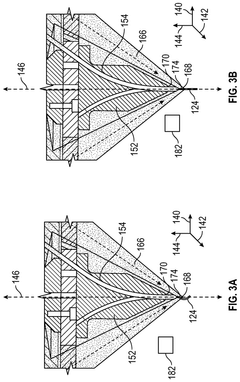
Directed Energy Deposition (DED) processes require precise control of various parameters to achieve optimal results. These parameters include laser power, deposition rate, material feed rate, and motion control. Advanced control systems can monitor and adjust these parameters in real-time to ensure consistent quality and dimensional accuracy. Process monitoring technologies such as thermal imaging and in-situ sensors help maintain process stability and detect anomalies during fabrication.- Process parameters and optimization for Directed Energy Deposition: Directed Energy Deposition (DED) processes require careful optimization of various parameters including laser power, deposition rate, material feed rate, and scanning speed. These parameters significantly influence the quality, microstructure, and mechanical properties of the fabricated components. Advanced control systems can be implemented to monitor and adjust these parameters in real-time, ensuring consistent quality throughout the build process. Optimization techniques may involve computational modeling and simulation to predict optimal parameter combinations for specific materials and geometries.
- Materials and powder characteristics for DED applications: The selection and preparation of materials for Directed Energy Deposition significantly impacts the success of the manufacturing process. Various metal powders, alloys, and composite materials can be used in DED processes, each requiring specific handling and processing conditions. Powder characteristics such as particle size distribution, flowability, and chemical composition must be carefully controlled to ensure consistent deposition. Pre-processing treatments and powder storage conditions also play important roles in maintaining material quality and preventing contamination that could lead to defects in the final components.
- Multi-material and functionally graded components using DED: Directed Energy Deposition technology enables the fabrication of multi-material and functionally graded components that cannot be produced using conventional manufacturing methods. By precisely controlling the material feed during the deposition process, it is possible to create components with varying material compositions throughout their structure. This capability allows for the design of parts with location-specific properties, such as wear resistance in certain areas and heat resistance in others. The technology can be used to produce components with smooth transitions between different materials, eliminating sharp interfaces that could become failure points under stress.
- Repair and remanufacturing applications of DED: Directed Energy Deposition is particularly valuable for repair and remanufacturing applications in industries such as aerospace, automotive, and heavy machinery. The technology allows for precise deposition of material onto existing components to restore damaged or worn surfaces. This capability extends the service life of high-value parts that would otherwise require complete replacement. The process can be tailored to match the original material properties and can be performed with minimal heat input to prevent distortion of the base component. Advanced monitoring systems can be integrated to ensure the repaired areas meet or exceed the specifications of the original part.
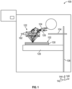
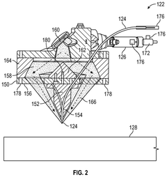
- Equipment and system design for DED processes: The design and configuration of Directed Energy Deposition systems significantly influence their capabilities and applications. Modern DED equipment may incorporate multiple energy sources, such as lasers or electron beams, with varying power levels and spot sizes to accommodate different materials and feature resolutions. Advanced systems often include multi-axis motion platforms that enable complex geometries and overhanging features without support structures. Closed-loop control systems with real-time monitoring capabilities can detect and correct process anomalies during fabrication. Specialized nozzle designs and gas shielding systems protect the melt pool from oxidation and contamination, particularly when processing reactive materials.
02 Material considerations for DED applications
The selection and preparation of materials significantly impact the success of Directed Energy Deposition processes. Various metal powders and wire feedstock can be used, including titanium alloys, nickel-based superalloys, and stainless steels. Material properties such as flowability, particle size distribution, and thermal characteristics must be optimized for specific DED techniques. Pre-processing treatments and post-processing heat treatments can enhance the mechanical properties and microstructure of the deposited material.Expand Specific Solutions03 Multi-material and functionally graded DED
Advanced Directed Energy Deposition techniques enable the fabrication of components with multiple materials or functionally graded properties. By controlling the composition of the feedstock during deposition, it's possible to create parts with varying material properties throughout their structure. This capability allows for optimized mechanical performance, thermal management, and wear resistance in specific regions of a component. Applications include aerospace components, tooling with wear-resistant surfaces, and biomedical implants with biocompatible surfaces.Expand Specific Solutions04 Hybrid manufacturing combining DED with machining
Hybrid manufacturing systems integrate Directed Energy Deposition with traditional machining processes in a single platform. This combination allows for additive building of features followed by subtractive finishing operations to achieve high dimensional accuracy and surface quality. The hybrid approach enables repair and modification of existing parts, reduces material waste, and shortens production time compared to conventional manufacturing methods. These systems typically incorporate CNC machining capabilities with laser or electron beam deposition technologies.Expand Specific Solutions05 DED equipment design and configuration
The design and configuration of Directed Energy Deposition equipment significantly influence process capabilities and part quality. Key components include the energy source (laser, electron beam, or plasma arc), material delivery system, motion control platform, and environmental control systems. Various nozzle designs optimize powder or wire delivery to the melt pool. Multi-axis systems enable complex geometries and overhanging features without support structures. Closed-loop feedback systems with integrated sensors allow for real-time process monitoring and adjustment during fabrication.Expand Specific Solutions
Key Industry Players in DED Electronics Applications
Directed Energy Deposition (DED) in advanced electronics is currently in a growth phase, with the market expanding due to increasing applications in precision manufacturing and component repair. The global market size is estimated to reach significant scale as industries recognize DED's potential for creating complex electronic structures with reduced material waste. Technologically, the field shows varying maturity levels across applications, with academic institutions (Katholieke Universiteit Leuven, California Institute of Technology, Swiss Federal Institute of Technology) leading fundamental research while commercial entities (Rolls-Royce, Xerox, Fabric8Labs) focus on practical implementations. Companies like Fabric8Labs are pioneering metal 3D printing technologies specifically for electronics applications, while established corporations such as Toyota and Honda are exploring DED for automotive electronics manufacturing, indicating a competitive landscape that spans both specialized startups and industrial giants.
California Institute of Technology
Technical Solution: California Institute of Technology (Caltech) has developed an innovative Quantum Dot Directed Energy Deposition (QD-DED) system specifically for next-generation optoelectronic applications. This technology utilizes precisely controlled energy beams to deposit semiconductor quantum dots and nanostructures with atomic-level precision. The system employs a proprietary multi-beam approach that combines electron beam lithography with molecular beam epitaxy techniques, allowing for the creation of three-dimensional quantum structures with tailored electronic and optical properties. Caltech's process incorporates in-situ characterization tools including scanning tunneling microscopy and photoluminescence spectroscopy to monitor quantum confinement effects during deposition. This enables real-time adjustments to achieve desired quantum energy levels in the fabricated structures. The technology has demonstrated particular success in creating quantum dot arrays for quantum computing applications, single-photon emitters for quantum cryptography, and advanced photodetectors with customized spectral responses. The QD-DED system operates in ultra-high vacuum conditions with temperature control from cryogenic to elevated temperatures, providing unprecedented control over quantum material synthesis.
Strengths: Atomic-level precision enables quantum-engineered electronic properties; in-situ characterization allows for real-time process optimization; capable of creating complex 3D quantum structures impossible with conventional techniques. Weaknesses: Extremely high vacuum requirements increase operational complexity; throughput is limited compared to conventional electronics manufacturing; requires specialized expertise in quantum materials science.
Naval Research Laboratory
Technical Solution: The Naval Research Laboratory has developed a specialized Directed Energy Deposition (DED) system for advanced electronics applications in harsh environments. Their technology, known as Plasma-Enhanced Directed Energy Deposition (PE-DED), utilizes a magnetically confined plasma beam to deposit high-purity electronic materials with exceptional adhesion and environmental resistance. The system incorporates a proprietary beam-focusing mechanism that achieves sub-10 micron resolution while maintaining deposition rates suitable for production environments. A key innovation is their multi-material feed system that allows for gradient material transitions, enabling the creation of components with spatially varying electrical properties. The PE-DED process operates at lower temperatures than conventional laser-based DED systems, reducing thermal stress on sensitive electronic substrates. This technology has been successfully deployed for creating radiation-hardened electronics for space applications and high-frequency components for advanced radar systems, demonstrating reliability in extreme conditions where conventional electronics would fail.
Strengths: Superior material adhesion and environmental durability; capable of creating gradient material transitions for specialized electronic properties; lower operating temperatures reduce substrate damage. Weaknesses: System requires specialized maintenance expertise; higher initial capital investment than conventional electronics manufacturing equipment; process optimization can be complex for new material combinations.
Critical Patents and Technical Literature Review
Wire oscillation for directed energy deposition
PatentPendingUS20250100077A1
Innovation
- A wire feed head with an integrated oscillator that oscillates either the feed wire or the energy source relative to each other, improving the average positional accuracy and power absorption by maintaining consistent wire exposure to the energy source.
Additive manufacturing method using a focused power source, said method being controlled according to the intensity of a control current of said focused power source
PatentActiveEP4129560A1
Innovation
- A method that monitors the intensity of the control current from a focused energy source, comparing it to a threshold, and temporarily stops the process when the intensity exceeds this threshold, then resumes once it falls below, ensuring the energy source and material supply are deactivated during high current conditions.
Material Compatibility and Performance Analysis
Material compatibility represents a critical factor in the successful implementation of Directed Energy Deposition (DED) processes for advanced electronics manufacturing. The interaction between the high-energy beam and various substrate materials creates unique challenges that must be thoroughly understood. Current research indicates that metallic substrates including copper, aluminum, and various alloys demonstrate varying degrees of compatibility with DED processes, with thermal conductivity and melting point being primary determinants of process success.
Performance analysis of DED-manufactured electronic components reveals promising results in terms of electrical conductivity, with some studies reporting conductivity levels reaching 85-95% of traditionally manufactured counterparts. This represents a significant advancement over earlier iterations of the technology, where conductivity rarely exceeded 70%. However, challenges persist in maintaining consistent performance across complex geometries and multi-material interfaces.
Thermal management capabilities of DED-produced components show notable improvements when specialized composite materials are incorporated. Recent experiments utilizing copper-graphene composites demonstrated a 30% enhancement in heat dissipation compared to standard copper components, suggesting potential applications in high-performance computing and power electronics where thermal management is paramount.
Mechanical integrity testing of DED-manufactured electronic components indicates satisfactory performance under standard operating conditions, with fatigue resistance comparable to conventional manufacturing methods. However, performance degradation accelerates under extreme temperature cycling, particularly at junction points between dissimilar materials. This limitation necessitates careful material selection and process optimization for applications requiring operation in harsh environments.
Surface finish quality remains a significant challenge, with as-deposited surfaces typically requiring post-processing to achieve the smoothness required for high-frequency electronic applications. Roughness values (Ra) for unprocessed DED surfaces generally range from 10-25 μm, significantly higher than the sub-micron requirements for many advanced electronic applications.
Corrosion resistance testing reveals variable performance depending on material composition and processing parameters. Aluminum-based components typically exhibit enhanced corrosion resistance compared to their traditionally manufactured counterparts, likely due to the formation of protective oxide layers during the high-temperature deposition process. Conversely, certain copper alloys show increased susceptibility to environmental degradation, necessitating protective coatings for long-term reliability.
Material-process parameter relationships have been established through extensive experimentation, with optimal energy density ranges identified for various electronic materials. These parameters must be carefully controlled to prevent defects such as porosity, cracking, and delamination that can significantly impact electronic performance and reliability.
Environmental Impact and Sustainability Considerations
The implementation of Directed Energy Deposition (DED) in advanced electronics manufacturing presents significant environmental and sustainability implications that warrant careful consideration. The process, while innovative for precision component fabrication, consumes substantial energy during operation—typically requiring high-powered lasers or electron beams that demand between 1-10 kW of power depending on application specifications. This energy intensity contributes to the carbon footprint of electronic device production, particularly when power sources rely on non-renewable energy.
Material efficiency represents a notable sustainability advantage of DED technology. Unlike traditional subtractive manufacturing methods that can waste up to 90% of raw materials, DED's additive approach significantly reduces material waste by depositing material only where needed. Studies indicate waste reduction of 30-60% compared to conventional electronics manufacturing processes, with particularly impressive results when working with precious metals and rare earth elements commonly used in advanced electronic components.
Water consumption during DED operations presents another environmental consideration. While the process itself requires minimal water compared to traditional chemical etching techniques, cooling systems for high-powered energy sources may consume significant quantities. Recent technological improvements have introduced closed-loop cooling systems that reduce water usage by approximately 40% compared to earlier DED implementations.
The environmental impact of feedstock materials used in DED processes must also be evaluated. The technology's compatibility with recycled materials offers promising sustainability benefits, with research demonstrating successful implementation using up to 30% recycled metal powders without significant performance degradation. This circular economy approach could substantially reduce the environmental burden associated with mining and refining virgin materials for electronics production.
End-of-life considerations for DED-manufactured components show mixed sustainability outcomes. The precise material deposition can create complex multi-material structures that present recycling challenges. However, the technology enables design optimizations that can extend product lifespan by 15-25% through improved thermal management and structural integrity, potentially offsetting recycling difficulties through extended product lifecycles.
Regulatory frameworks addressing the environmental aspects of DED implementation are evolving globally. The European Union's Eco-design Directive and Restriction of Hazardous Substances (RoHS) regulations increasingly influence manufacturing process selection, with DED technologies generally aligning well with requirements for reduced material waste and energy efficiency when properly optimized and implemented with sustainability considerations at the forefront.
Unlock deeper insights with Patsnap Eureka Quick Research — get a full tech report to explore trends and direct your research. Try now!
Generate Your Research Report Instantly with AI Agent
Supercharge your innovation with Patsnap Eureka AI Agent Platform!