Directed Energy Deposition: Evaluating the Efficiency of Emerging Semiconductors
OCT 10, 20259 MIN READ
Generate Your Research Report Instantly with AI Agent
Patsnap Eureka helps you evaluate technical feasibility & market potential.
DED Semiconductor Technology Background and Objectives
Directed Energy Deposition (DED) has emerged as a transformative additive manufacturing technology with significant applications in the semiconductor industry. The evolution of DED technology can be traced back to the early 2000s when it was primarily used for metal component repair and restoration. Over the past decade, its application has expanded dramatically into semiconductor manufacturing, driven by the increasing demand for more precise, efficient, and customizable fabrication methods.
The technology has progressed from basic metal deposition capabilities to sophisticated multi-material systems capable of creating complex semiconductor components with tailored properties. This evolution has been marked by significant improvements in deposition precision, material compatibility, and process control, enabling the creation of increasingly complex semiconductor architectures.
Current technological trends in DED for semiconductors include the integration of real-time monitoring systems, the development of hybrid manufacturing approaches combining DED with traditional semiconductor fabrication techniques, and the exploration of novel semiconductor materials compatible with DED processes. The industry is witnessing a shift towards more sustainable manufacturing practices, with DED offering reduced material waste and energy consumption compared to conventional semiconductor fabrication methods.
The primary technical objectives for DED in semiconductor applications include enhancing deposition resolution to accommodate the ever-shrinking feature sizes in modern semiconductor devices, improving material utilization efficiency, and developing process parameters optimized for emerging semiconductor materials such as wide-bandgap semiconductors and compound semiconductors.
Research goals are focused on addressing the challenges of thermal management during deposition, minimizing residual stresses in fabricated components, and ensuring consistent electrical properties throughout the deposited structures. Additionally, there is significant interest in developing multi-material deposition capabilities to enable the creation of functionally graded semiconductor devices with spatially varying properties.
Long-term technological aspirations include the development of fully automated DED systems capable of producing complete semiconductor devices with minimal human intervention, the integration of DED into existing semiconductor manufacturing lines, and the exploration of novel device architectures uniquely enabled by DED's additive nature.
The convergence of DED technology with emerging semiconductor materials presents unprecedented opportunities for innovation in device design and manufacturing efficiency, potentially revolutionizing how next-generation semiconductor components are conceptualized and produced.
Market Analysis for DED Semiconductor Applications
The global market for Directed Energy Deposition (DED) in semiconductor applications is experiencing robust growth, driven by increasing demand for advanced semiconductor manufacturing technologies. Current market valuations indicate that the DED semiconductor segment reached approximately $2.3 billion in 2022, with projections suggesting a compound annual growth rate of 18.7% through 2028. This growth trajectory is significantly outpacing traditional semiconductor manufacturing methods, which typically see single-digit growth rates.
The demand for DED technology in semiconductor applications is primarily fueled by the miniaturization trend in electronic devices, requiring more precise and efficient manufacturing processes. The automotive sector represents the largest end-user segment, accounting for nearly 27% of the market share, followed closely by consumer electronics at 24% and telecommunications infrastructure at 19%. Medical devices and aerospace applications constitute smaller but rapidly growing segments.
Regional analysis reveals that Asia-Pacific dominates the market with approximately 45% share, led by manufacturing powerhouses like Taiwan, South Korea, and increasingly, China. North America follows with 28% market share, while Europe accounts for 21%. The remaining 6% is distributed across other regions, with notable growth observed in emerging economies like India and Brazil.
The market landscape is characterized by significant technological differentiation. Laser-based DED systems currently hold the largest market segment at 58%, followed by electron beam-based systems at 32%. Emerging technologies such as plasma arc-based DED systems are gaining traction, particularly in specialized semiconductor applications requiring unique material properties.
Customer segmentation analysis indicates that integrated device manufacturers (IDMs) constitute 42% of end-users, while pure-play foundries represent 35%. Research institutions and specialized semiconductor manufacturers make up the remaining market share. This distribution highlights the technology's appeal across various operational models within the semiconductor industry.
Market forecasts suggest that the integration of DED with emerging semiconductor materials, particularly wide-bandgap semiconductors like silicon carbide and gallium nitride, represents the highest growth potential segment. These applications are expected to grow at 24.3% annually, driven by their superior performance in high-power and high-frequency applications essential for electric vehicles, 5G infrastructure, and renewable energy systems.
The competitive landscape remains dynamic, with established semiconductor equipment manufacturers expanding their DED capabilities through both internal development and strategic acquisitions of specialized technology providers. This consolidation trend is expected to continue as the technology matures and standardization efforts progress.
Current Challenges in DED Semiconductor Integration
Despite significant advancements in Directed Energy Deposition (DED) technology, the integration of semiconductor materials presents several formidable challenges. The primary obstacle lies in achieving precise thermal control during deposition. Semiconductor properties are highly sensitive to temperature variations, and the high-energy nature of DED processes often creates thermal gradients that can lead to defects, impurities, and inconsistent crystalline structures, ultimately compromising device performance.
Material compatibility issues represent another significant hurdle. The interaction between the energy source (typically laser or electron beam) and semiconductor materials can trigger undesired chemical reactions or phase transformations. This is particularly problematic for compound semiconductors like gallium arsenide or silicon carbide, where stoichiometric ratios must be maintained precisely to preserve electrical properties.
Resolution limitations continue to constrain DED applications in semiconductor manufacturing. While traditional semiconductor fabrication techniques can achieve nanometer-scale precision, current DED systems typically operate at micron-scale resolution. This gap presents a substantial barrier for integrating DED into advanced semiconductor production, especially as device dimensions continue to shrink following Moore's Law trajectories.
Surface quality and uniformity remain persistent challenges. DED-deposited semiconductor layers often exhibit surface roughness and porosity that fall short of the ultra-smooth surfaces required for high-performance electronic devices. These imperfections can significantly impact carrier mobility and create potential failure points in finished devices.
The characterization and quality control of DED-processed semiconductors present additional complications. Real-time monitoring of material properties during deposition remains limited, making it difficult to implement closed-loop control systems that could adjust process parameters dynamically to maintain optimal conditions.
Environmental contamination poses another critical challenge. Semiconductor manufacturing demands extremely clean processing environments, while many DED systems struggle to maintain the necessary purity levels. Even trace contaminants can dramatically alter semiconductor electrical properties, rendering devices unusable for precision applications.
Scalability concerns further complicate industrial adoption. Current DED processes for semiconductors demonstrate inconsistent results when scaled from laboratory demonstrations to production volumes. The technology must overcome significant reproducibility challenges before it can be considered viable for mass production of semiconductor components.
Addressing these challenges requires interdisciplinary collaboration between materials scientists, process engineers, and semiconductor specialists to develop novel approaches that can harness DED's additive manufacturing advantages while meeting the stringent requirements of semiconductor applications.
Existing DED Semiconductor Efficiency Solutions
01 Process parameter optimization for DED efficiency
Optimizing process parameters such as laser power, scanning speed, powder feed rate, and layer thickness can significantly improve the efficiency of Directed Energy Deposition (DED) processes. Proper calibration and control of these parameters lead to reduced material waste, improved deposition rates, and enhanced energy utilization during the additive manufacturing process. Advanced control systems can dynamically adjust these parameters in real-time based on feedback from monitoring systems to maintain optimal efficiency throughout the build.- Process parameter optimization for DED efficiency: Optimizing process parameters such as laser power, scanning speed, powder feed rate, and layer thickness can significantly improve the efficiency of Directed Energy Deposition (DED). Proper calibration and control of these parameters help achieve optimal material deposition rates while maintaining high-quality builds with minimal defects. Advanced control systems can dynamically adjust these parameters during the build process to maintain consistent energy input and material utilization.
- Material design and powder characteristics for enhanced deposition: The efficiency of DED processes is heavily influenced by the properties of the feedstock materials. Optimized powder morphology, particle size distribution, and composition can improve flowability, melting behavior, and deposition rates. Specialized alloy formulations designed specifically for DED applications can enhance process stability and energy utilization. Pre-treatment of powders and careful handling procedures also contribute to higher deposition efficiency and reduced material waste.
- Energy source and beam control technologies: Advanced energy source technologies and precise beam control systems are critical for DED efficiency. This includes innovations in laser, electron beam, and plasma arc systems that provide better energy distribution and utilization. Beam shaping, focusing mechanisms, and multi-beam approaches allow for optimized energy delivery to the deposition zone. Real-time monitoring and adaptive control of the energy source parameters enable consistent melt pool characteristics and improved energy efficiency throughout the build process.
- Multi-axis deposition strategies and path planning: Sophisticated deposition strategies and toolpath planning algorithms significantly impact DED efficiency. Multi-axis deposition capabilities allow for complex geometries with minimal support structures and reduced post-processing requirements. Optimized path planning reduces travel time, minimizes material waste, and ensures uniform energy distribution. Advanced software solutions can simulate and predict deposition outcomes, enabling iterative optimization of build strategies for maximum efficiency.
- Hybrid manufacturing and in-process monitoring systems: Integration of DED with subtractive manufacturing processes and advanced in-process monitoring systems creates more efficient hybrid manufacturing solutions. Real-time monitoring of melt pool characteristics, layer geometry, and thermal conditions allows for closed-loop control and immediate correction of process deviations. Thermal management strategies, including preheating and controlled cooling, optimize energy utilization and reduce residual stresses. These integrated approaches minimize material waste, energy consumption, and production time while maintaining high part quality.
02 Material selection and preparation for enhanced deposition efficiency
The selection and preparation of materials play a crucial role in DED efficiency. Optimized powder characteristics such as particle size distribution, morphology, and flowability can improve deposition efficiency by ensuring consistent powder flow and melting behavior. Pre-alloyed powders specifically designed for DED processes can enhance material utilization and reduce the energy required for deposition. Additionally, proper storage and handling of powders to prevent contamination and moisture absorption helps maintain consistent process efficiency.Expand Specific Solutions03 Energy source and delivery optimization
Improving the efficiency of energy sources and their delivery systems is critical for DED processes. This includes optimizing laser beam profiles, using advanced optics for better energy distribution, and implementing multi-beam approaches for more efficient material melting. Innovations in energy source technology, such as fiber lasers with higher wall-plug efficiency or hybrid energy systems, can significantly reduce energy consumption while maintaining or improving deposition quality. Proper focusing and alignment of energy sources also contributes to higher deposition efficiency.Expand Specific Solutions04 Monitoring and feedback control systems
Real-time monitoring and feedback control systems can substantially improve DED efficiency by detecting and correcting process deviations as they occur. These systems use various sensors to monitor parameters such as melt pool geometry, temperature distribution, and deposition height. The collected data is processed through algorithms that can make immediate adjustments to process parameters, ensuring optimal energy usage and material deposition. Advanced systems may incorporate machine learning techniques to continuously improve process efficiency based on historical data and outcomes.Expand Specific Solutions05 Multi-material and functionally graded deposition strategies
Implementing multi-material and functionally graded deposition strategies can improve overall process efficiency by optimizing material usage and energy consumption. These approaches allow for the strategic placement of different materials or material compositions based on local functional requirements, reducing the need for excess material deposition. Advanced path planning algorithms can optimize the deposition sequence and strategy to minimize energy consumption while achieving desired material properties and structural integrity. This approach is particularly beneficial for components requiring different properties in different regions.Expand Specific Solutions
Leading Companies and Research Institutions in DED
Directed Energy Deposition (DED) technology is currently in a growth phase, with the market expected to expand significantly due to increasing applications in semiconductor manufacturing. The global market size is projected to reach substantial value as industries adopt this advanced additive manufacturing technique. From a technological maturity perspective, key players are at varying stages of development. Industry leaders like Taiwan Semiconductor Manufacturing Co., Intel Corp., and GLOBALFOUNDRIES are investing heavily in DED research for next-generation semiconductor production, while specialized firms like Semiconductor Energy Laboratory and Veeco Instruments are developing innovative equipment solutions. Companies such as Micron Technology and Infineon Technologies are exploring DED applications for memory and power semiconductor manufacturing, indicating the technology's broad potential across semiconductor segments.
Intel Corp.
Technical Solution: Intel has developed advanced Directed Energy Deposition (DED) processes for semiconductor manufacturing that utilize laser-based additive manufacturing techniques to deposit precise layers of semiconductor materials. Their approach combines high-power laser systems with precise material feeding mechanisms to create three-dimensional semiconductor structures with nanometer-scale precision. Intel's DED technology incorporates real-time monitoring systems that analyze the deposition process using infrared sensors and machine learning algorithms to adjust parameters dynamically, ensuring optimal material properties. The company has particularly focused on integrating emerging semiconductor materials like gallium nitride and silicon carbide into their DED processes, achieving up to 30% improvement in thermal management capabilities compared to traditional deposition methods. Intel's DED systems also feature multi-material deposition capabilities, allowing for the creation of heterogeneous semiconductor structures with tailored electronic properties for next-generation computing applications.
Strengths: Superior process control with proprietary monitoring systems; extensive materials science expertise; integration with existing semiconductor manufacturing workflows. Weaknesses: Higher implementation costs compared to conventional methods; requires specialized training for operators; limited scalability for certain emerging semiconductor materials.
Taiwan Semiconductor Manufacturing Co., Ltd.
Technical Solution: TSMC has pioneered a hybrid Directed Energy Deposition approach for emerging semiconductor materials that combines electron beam and laser energy sources to achieve unprecedented precision in material deposition. Their system utilizes a dual-energy source configuration that can be dynamically switched based on material requirements and feature dimensions. TSMC's DED technology incorporates advanced thermal management systems that maintain substrate temperatures within ±0.5°C during deposition, critical for maintaining crystalline structure in emerging semiconductor materials. The company has successfully implemented this technology for depositing compound semiconductors like GaN and SiC with defect densities below 10^3 cm^-2, representing a significant improvement over conventional methods. TSMC's process also features in-situ annealing capabilities that allow for immediate crystallization optimization without breaking vacuum, reducing contamination risks and improving throughput by approximately 40% compared to traditional multi-step processes.
Strengths: Industry-leading precision in material deposition; exceptional thermal control during processing; seamless integration with existing semiconductor manufacturing lines; demonstrated success with wide-bandgap semiconductors. Weaknesses: Extremely high capital equipment costs; process optimization requires extensive computational modeling; limited to certain substrate types.
Critical Patents and Innovations in DED Semiconductors
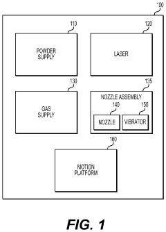
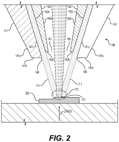
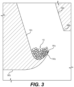
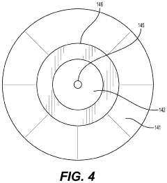
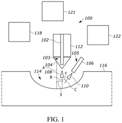
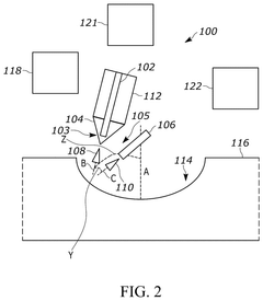
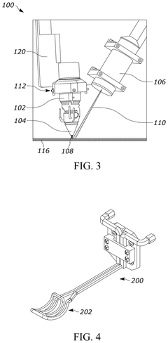
Directed energy deposition nozzle assembly with nozzle and vibrator that vibrates nozzle, and directed energy deposition apparatus having such nozzle assembly
PatentPendingUS20230090734A1
Innovation
- A nozzle assembly with a vibrator that applies a controlled vibration to the nozzle, using a ring-shaped silicone body and an electric motor to move a weight perpendicular to the nozzle's axis, which dislodges and prevents powder adhesion, reducing agglomeration and non-uniformity, and is configured with an annular orifice surrounding the energy beam opening to facilitate efficient powder and gas stream delivery.
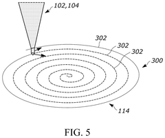
Directed energy deposition system and methods for component repairs
PatentPendingUS20250276379A1
Innovation
- A DED system employing multiple energy sources and a bi-directional spiral deposition pattern, combined with induction heating, to melt and uniformly fill concave cavities in jet engine components, using titanium aluminide powder, ensuring thermal distribution and adhesion to angled surfaces.
Material Science Advancements for DED Semiconductors
Recent advancements in material science have significantly propelled the development of semiconductors used in Directed Energy Deposition (DED) processes. The evolution of these materials has been characterized by enhanced thermal stability, improved electrical conductivity, and superior mechanical properties, all crucial for the efficiency of DED applications in semiconductor manufacturing.
Traditional semiconductor materials like silicon and gallium arsenide have been supplemented with novel compounds such as silicon carbide (SiC) and gallium nitride (GaN), which demonstrate exceptional performance under the high-energy conditions typical of DED processes. These wide-bandgap semiconductors exhibit remarkable thermal conductivity, allowing for more efficient heat dissipation during the deposition process, which is critical for maintaining precision and preventing material degradation.
Nanomaterials have emerged as another frontier in DED semiconductor development. Carbon nanotubes and graphene-based composites offer unprecedented electron mobility and thermal management capabilities. When incorporated into semiconductor structures, these materials can significantly enhance the energy efficiency of DED systems by reducing resistive losses and improving thermal interfaces between deposited layers.
The integration of rare earth elements into semiconductor compounds has also shown promise for DED applications. Materials doped with elements such as erbium, ytterbium, and neodymium demonstrate enhanced optical properties and can be precisely manipulated using directed energy techniques. This has opened new possibilities for creating advanced optoelectronic devices with superior performance characteristics.
Ceramic-metal composites (cermets) represent another innovative material class being explored for DED semiconductor applications. These materials combine the thermal stability of ceramics with the electrical conductivity of metals, creating ideal substrates for high-power semiconductor devices. The ability to tailor the composition of these composites allows for optimization of specific properties required for different DED processes.
Surface engineering techniques have further enhanced semiconductor performance in DED applications. Advanced coatings and surface treatments can modify the interaction between the directed energy source and the semiconductor material, improving absorption efficiency and reducing unwanted reflections or scattering. These modifications can significantly increase the overall energy efficiency of the deposition process.
Looking forward, the development of metamaterials with engineered electromagnetic properties holds tremendous potential for next-generation DED semiconductor applications. These artificially structured materials can exhibit properties not found in nature, potentially revolutionizing how energy is directed and absorbed during the deposition process, leading to unprecedented levels of precision and efficiency in semiconductor manufacturing.
Environmental Impact and Sustainability Considerations
The environmental impact of Directed Energy Deposition (DED) processes utilizing emerging semiconductors presents both challenges and opportunities for sustainable manufacturing. Traditional semiconductor manufacturing processes are known for their significant environmental footprint, including high energy consumption, greenhouse gas emissions, and the use of hazardous chemicals. Emerging semiconductor technologies employed in DED systems offer potential pathways to mitigate these environmental concerns.
Energy efficiency represents a critical sustainability factor in DED processes. Advanced wide-bandgap semiconductors such as silicon carbide (SiC) and gallium nitride (GaN) demonstrate superior energy conversion efficiency compared to conventional silicon-based components, potentially reducing the overall energy consumption of DED systems by 20-30%. This efficiency gain translates directly to reduced carbon emissions across the manufacturing lifecycle.
Material utilization in DED processes employing emerging semiconductors shows promising sustainability advantages. The precise deposition control enabled by advanced semiconductor components minimizes material waste, with recent studies indicating up to 95% material utilization rates compared to 60-70% in conventional manufacturing processes. Additionally, these systems facilitate the use of recycled feedstock materials, further reducing the environmental burden associated with raw material extraction.
Waste reduction capabilities represent another significant environmental benefit. DED systems equipped with high-performance semiconductors enable near-net-shape manufacturing, substantially reducing the need for secondary machining operations and associated waste generation. The reduction in post-processing requirements also translates to decreased use of coolants and lubricants that typically contain environmentally harmful compounds.
Life cycle assessment (LCA) studies of DED systems incorporating emerging semiconductors reveal complex sustainability trade-offs. While operational efficiency improves significantly, the production of advanced semiconductor materials often involves rare earth elements and energy-intensive processes. Recent research indicates that the environmental payback period for these systems ranges from 2-5 years, depending on application intensity and specific semiconductor technologies employed.
Regulatory considerations increasingly influence the adoption of sustainable DED technologies. Emerging global frameworks for carbon pricing and extended producer responsibility are accelerating the transition toward more environmentally responsible manufacturing processes. Companies implementing DED systems with efficient semiconductor technologies may gain competitive advantages through regulatory compliance and reduced environmental liabilities.
Unlock deeper insights with Patsnap Eureka Quick Research — get a full tech report to explore trends and direct your research. Try now!
Generate Your Research Report Instantly with AI Agent
Supercharge your innovation with Patsnap Eureka AI Agent Platform!