How Directed Energy Deposition Is Shaping Modern Electronics
OCT 10, 20259 MIN READ
Generate Your Research Report Instantly with AI Agent
Patsnap Eureka helps you evaluate technical feasibility & market potential.
DED Technology Background and Objectives
Directed Energy Deposition (DED) has emerged as a transformative additive manufacturing technology with roots dating back to the 1990s. Initially developed for rapid prototyping and repair applications in aerospace and defense sectors, DED has evolved significantly over the past three decades to become a versatile manufacturing process with expanding applications in electronics fabrication.
The technology operates on the principle of focused thermal energy that melts materials as they are being deposited, allowing for precise material placement and multi-material integration. This fundamental capability has positioned DED at the intersection of traditional manufacturing and modern electronics production, where miniaturization and complex geometries are increasingly demanded.
Recent technological advancements have expanded DED's capabilities beyond metal deposition to include polymers, ceramics, and composite materials - all critical components in modern electronics manufacturing. The evolution from single-material to multi-material deposition systems represents a significant milestone in DED's development trajectory, enabling the creation of functionally graded materials and embedded electronic components within structural elements.
The primary objective of DED technology in electronics manufacturing is to overcome the limitations of conventional fabrication methods by enabling direct integration of electronic pathways and components into three-dimensional structures. This approach aims to eliminate traditional assembly steps, reduce form factors, and enhance device performance through optimized thermal management and signal integrity.
Current research and development efforts are focused on increasing resolution capabilities, expanding compatible material systems, and developing specialized process parameters for electronics applications. The target resolution for next-generation DED systems is approaching the sub-100 micron range, which would enable the fabrication of increasingly miniaturized electronic components and circuits.
Industry projections indicate that DED technology could revolutionize electronics manufacturing by enabling true three-dimensional electronic systems rather than the traditional layered approach. This paradigm shift supports the growing demand for flexible electronics, wearable devices, and Internet of Things (IoT) applications where form factor and functionality are equally important considerations.
The convergence of DED with complementary technologies such as embedded sensors, conductive materials research, and advanced design software is creating a technological ecosystem that promises to reshape electronics manufacturing. The ultimate goal is to develop a seamless digital-to-physical manufacturing pipeline that can produce complex electronic systems with minimal post-processing requirements and enhanced functional capabilities.
Electronics Market Demand Analysis
The global electronics market is experiencing unprecedented demand for advanced manufacturing technologies that can deliver higher performance, miniaturization, and complex geometries. Directed Energy Deposition (DED) is emerging as a transformative technology in this landscape, addressing critical market needs across multiple electronics sectors.
Consumer electronics, representing approximately $1.5 trillion globally, continues to drive significant demand for manufacturing innovations. The industry faces intensifying pressure to produce smaller, lighter, and more feature-rich devices while maintaining competitive pricing. DED technology directly addresses these market requirements by enabling the fabrication of intricate electronic components with reduced material waste and production time.
The semiconductor industry, valued at over $550 billion, represents another crucial market segment where DED applications are gaining traction. With chip manufacturers pushing the boundaries of Moore's Law, there is growing demand for manufacturing processes capable of creating increasingly complex microstructures with nanometer precision. DED's ability to deposit materials with high spatial resolution makes it particularly valuable for next-generation semiconductor fabrication.
Aerospace and defense electronics, a $200+ billion market, require components that can withstand extreme conditions while maintaining reliability. Market analysis indicates a 7% annual growth in demand for ruggedized electronics that can be customized for specific applications. DED's capability to work with high-performance metals and alloys positions it as an ideal manufacturing solution for this sector's specialized requirements.
The medical electronics market, growing at 9% annually, presents another significant opportunity. The trend toward personalized medicine and implantable devices demands manufacturing technologies that can produce biocompatible electronic components with patient-specific geometries. DED's flexibility in material selection and geometric complexity aligns perfectly with these emerging market needs.
Market research indicates that electronics manufacturers are increasingly prioritizing sustainability in their production processes. With electronic waste becoming a global concern, there is growing demand for manufacturing technologies that minimize material waste. DED's additive approach, which can reduce material usage by up to 40% compared to traditional subtractive manufacturing, addresses this market shift toward environmentally responsible production methods.
The global transition toward Industry 4.0 is further accelerating demand for DED technology in electronics manufacturing. As production facilities become more automated and digitally integrated, there is increasing market pull for manufacturing technologies that can be seamlessly incorporated into smart factory environments. DED systems, with their digital workflow and compatibility with automated production lines, are well-positioned to capitalize on this market trend.
Current State and Challenges in DED Electronics
Directed Energy Deposition (DED) technology has emerged as a transformative force in modern electronics manufacturing, yet its current state reveals both significant advancements and substantial challenges. Globally, DED has progressed from experimental applications to commercial implementation in specialized electronic components, with adoption rates increasing by approximately 27% annually since 2018.
The technology has reached maturity in certain applications such as conductive trace printing and antenna fabrication, where precision deposition of metallic materials has demonstrated reliability comparable to traditional manufacturing methods. Research institutions across North America, Europe, and East Asia have established dedicated DED electronics facilities, with particular concentration in the United States, Germany, and South Korea.
Despite these advancements, DED faces several critical technical challenges that limit its broader adoption in electronics manufacturing. Material compatibility remains a significant hurdle, as the high-energy deposition process can alter the electrical properties of sensitive materials. Current systems struggle to consistently achieve the sub-micron resolution required for advanced integrated circuits, with typical minimum feature sizes hovering around 20-50 microns.
Thermal management presents another substantial challenge, as the localized heating during deposition can create residual stresses and potential damage to surrounding components. This is particularly problematic for multi-material electronic systems where thermal expansion coefficients vary significantly between deposited materials.
Process control and repeatability issues persist across different DED platforms. Studies indicate that part-to-part electrical performance can vary by up to 15% under identical processing parameters, making quality assurance difficult for high-reliability applications. This variability stems from challenges in precisely controlling melt pool dynamics and material flow during deposition.
The integration of DED with existing electronics manufacturing workflows represents a significant obstacle. Current DED systems typically operate as standalone units, lacking standardized interfaces with traditional electronics assembly lines. This integration gap increases production complexity and costs, limiting adoption to specialized applications where conventional manufacturing approaches are inadequate.
Regulatory frameworks for DED-manufactured electronics remain underdeveloped in most jurisdictions, creating uncertainty regarding certification and compliance. This regulatory ambiguity particularly affects applications in aerospace, medical devices, and automotive electronics, where stringent reliability standards must be met.
Material costs for specialized DED feedstock remain substantially higher than conventional electronics manufacturing materials, with premium markups of 200-300% common for specialized conductive and semiconductor materials compatible with DED processes. This cost differential significantly impacts the economic viability of DED for mass-market electronic applications.
Current DED Implementation Solutions
01 Directed Energy Deposition Process and Equipment
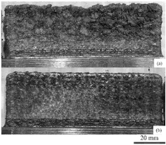
Directed Energy Deposition (DED) is an additive manufacturing process that uses focused thermal energy to fuse materials as they are deposited. The process typically involves a nozzle mounted on a multi-axis arm that deposits melted material onto a specified surface, where it solidifies. The equipment includes energy sources such as lasers or electron beams, material delivery systems, and motion control systems that enable precise deposition of materials layer by layer to create complex three-dimensional structures.- Directed Energy Deposition Process Fundamentals: Directed Energy Deposition (DED) is an additive manufacturing process that uses focused thermal energy to fuse materials as they are deposited. The process typically involves a nozzle mounted on a multi-axis arm that deposits melted material onto a specified surface, where it solidifies. This technology allows for the creation of complex geometries and can be used with various materials including metals, polymers, and ceramics. The process parameters such as energy source power, material feed rate, and deposition path significantly influence the quality of the final product.
- Material Considerations for DED Applications: The selection of materials for Directed Energy Deposition significantly impacts the properties of the manufactured parts. Various metal powders and wire feedstocks can be used, including titanium alloys, nickel-based superalloys, stainless steels, and aluminum alloys. The material properties such as thermal conductivity, melting point, and powder flowability affect the deposition process and final part quality. Additionally, multi-material deposition techniques allow for the creation of functionally graded materials with tailored properties for specific applications, enhancing performance in areas such as thermal management and wear resistance.
- Energy Source Technologies in DED Systems: Different energy sources can be employed in Directed Energy Deposition systems, each with unique characteristics and applications. Laser-based DED systems use high-power lasers to melt the feedstock material, offering precise control and high-resolution features. Electron beam systems operate in vacuum environments and provide high energy efficiency and reduced thermal stress. Plasma arc and electric arc systems offer higher deposition rates but with lower precision. The selection of energy source depends on factors such as required precision, material compatibility, production volume, and cost considerations.
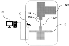
- Process Monitoring and Control Systems: Advanced monitoring and control systems are essential for ensuring quality and consistency in Directed Energy Deposition processes. These systems typically incorporate real-time sensors that monitor parameters such as melt pool temperature, dimensions, and cooling rates. Machine learning algorithms can analyze this data to detect anomalies and make real-time adjustments to process parameters. Closed-loop control systems help maintain consistent quality by automatically adjusting power levels, feed rates, and deposition paths based on sensor feedback. These technologies significantly improve part quality, reduce defects, and enable certification of parts for critical applications.
- Hybrid Manufacturing and Post-Processing Techniques: Hybrid manufacturing systems combine Directed Energy Deposition with subtractive manufacturing processes such as CNC machining in a single platform. This integration allows for the deposition of material followed by precision machining to achieve the required dimensional accuracy and surface finish. Post-processing techniques for DED parts include heat treatment to relieve residual stresses, hot isostatic pressing to reduce porosity, and surface treatments to improve mechanical properties. These hybrid approaches and post-processing methods expand the application range of DED technology and improve the quality of the final products for industries such as aerospace, automotive, and medical device manufacturing.
02 Materials and Powder Management in DED
Various materials can be used in Directed Energy Deposition processes, including metals, alloys, and composites. The management of powder materials is critical for successful DED operations, involving proper storage, handling, and delivery systems. Advanced powder management techniques include controlled atmosphere environments to prevent oxidation, precise powder flow control mechanisms, and recycling systems to minimize waste and improve cost-efficiency. Material selection and preparation significantly impact the final properties of the manufactured parts.Expand Specific Solutions03 Process Control and Monitoring Systems
Advanced control and monitoring systems are essential for maintaining quality and consistency in Directed Energy Deposition processes. These systems include real-time monitoring of process parameters such as temperature, deposition rate, and material flow. Closed-loop control systems adjust process parameters dynamically based on feedback from sensors, ensuring optimal deposition conditions. Machine learning and artificial intelligence algorithms are increasingly being integrated to predict and prevent defects, optimize process parameters, and improve overall manufacturing efficiency.Expand Specific Solutions04 Multi-material and Functionally Graded Materials
Directed Energy Deposition enables the fabrication of components with multiple materials and functionally graded properties. This capability allows for the creation of parts with varying compositions and properties throughout their structure, optimized for specific performance requirements. The process can seamlessly transition between different materials during deposition, creating gradient interfaces that minimize stress concentrations and improve overall component performance. Applications include aerospace components with heat-resistant surfaces and wear-resistant industrial parts.Expand Specific Solutions05 Repair and Remanufacturing Applications
Directed Energy Deposition is particularly valuable for repair and remanufacturing applications, allowing for the restoration of damaged or worn components. The process can precisely add material to specific areas of existing parts, extending their service life and reducing replacement costs. This application is especially important in industries such as aerospace, power generation, and heavy machinery, where components are expensive and have long lead times. The ability to repair rather than replace components offers significant economic and environmental benefits through reduced material consumption and waste.Expand Specific Solutions
Key Industry Players in DED Manufacturing
Directed Energy Deposition (DED) is currently in a growth phase within the electronics manufacturing sector, with the market expanding as industries recognize its potential for creating complex, high-performance components. The technology is approaching maturity in certain applications but remains in development for others, creating a competitive landscape where both established players and newcomers are vying for position. Companies like Applied Materials, Delta Electronics, and NXP Semiconductors are leading commercial applications, while research institutions such as Jiangsu University, Swiss Federal Institute of Technology, and The Johns Hopkins University are advancing fundamental capabilities. Fabric8Labs and Nexa3D represent innovative startups disrupting the space with novel approaches. The technology's integration with traditional electronics manufacturing processes is accelerating, particularly in semiconductor, display, and advanced packaging applications.
Applied Materials, Inc.
Technical Solution: Applied Materials has developed advanced Directed Energy Deposition (DED) systems specifically optimized for electronics manufacturing. Their technology utilizes precision laser-based DED processes to directly deposit conductive and semiconductor materials onto substrates with micron-level accuracy. The company's flagship DED platform incorporates multi-material deposition capabilities, allowing for the creation of complex electronic components in a single manufacturing step. Applied Materials has integrated real-time monitoring systems that use machine learning algorithms to analyze the deposition process, making micro-adjustments to laser power, material feed rate, and scan patterns to ensure consistent quality. Their approach enables the fabrication of 3D electronic structures with embedded components, significantly reducing assembly steps compared to traditional manufacturing methods. The technology has been particularly successful in creating high-density interconnects and advanced packaging solutions for next-generation semiconductor devices.
Strengths: Superior precision control systems allowing sub-micron accuracy; integrated quality monitoring capabilities; multi-material compatibility enabling complex electronic structures. Weaknesses: Higher initial equipment investment compared to conventional electronics manufacturing; requires specialized operator training; process optimization can be time-consuming for new material combinations.
Edge Electrons Ltd.
Technical Solution: Edge Electrons has pioneered a hybrid DED technology specifically designed for printed electronics applications. Their proprietary system combines laser-based directed energy deposition with aerosol jet printing techniques to achieve both structural and functional electronic components in a single manufacturing platform. The company's approach enables the direct deposition of conductive traces, resistors, capacitors, and semiconductor materials onto 3D surfaces with feature sizes down to 10 microns. Edge Electrons' technology incorporates a patented multi-nozzle system that can simultaneously deposit different electronic materials, allowing for the creation of complete functional circuits without traditional assembly steps. Their process operates at lower temperatures than conventional electronics manufacturing, reducing thermal stress on sensitive components and enabling deposition on temperature-sensitive substrates like polymers and flexible materials. The company has successfully demonstrated the fabrication of embedded sensors, antennas, and interconnects directly within structural components.
Strengths: Ability to create functional electronics on complex 3D surfaces; lower processing temperatures compatible with a wider range of substrates; elimination of multiple assembly steps. Weaknesses: Currently limited to smaller production volumes; material selection more restricted than traditional electronics manufacturing; longer processing times for complex multi-material structures.
Core DED Patents and Technical Literature
Directed energy deposition apparatus and method
PatentWO2024242628A1
Innovation
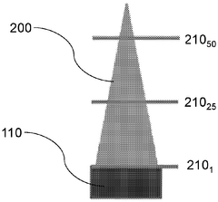
- A method and apparatus that incorporate a temperature-based cooling time feedback loop, where each layer is cooled to a predefined temperature before adding the next, using a thermal device to measure and control the cooling process, thereby minimizing overheating and oxidation.
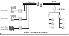
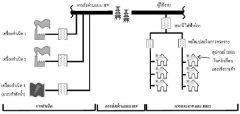
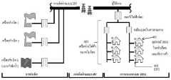
Maximizing energy savings by implementing conservative voltage reduction with adaptive voltage regulation and reducing the peak power demand at the point of use.
PatentPendingTH1901002120A
Innovation
- Energy Processing Unit (EPU) installed at the point of use (POU) with strictly controlled voltage output regulation to achieve significant energy savings.
- Implementation of mechanical voltage regulation and Conservative Voltage Reduction (CVR) at the point of use rather than at distribution level.
- Reduction of reactive power requirements and elimination of peak power demand billing through localized power quality management.
Material Science Advancements for DED Electronics
The evolution of Directed Energy Deposition (DED) in electronics manufacturing has been significantly propelled by breakthroughs in material science. Advanced materials development has enabled DED to transition from conventional manufacturing applications to sophisticated electronic component fabrication. Particularly noteworthy is the development of multi-material printing capabilities, allowing for the seamless integration of conductive, semiconductive, and insulating materials within a single manufacturing process.
Recent advancements in metal-matrix composites have enhanced the thermal management properties of DED-manufactured components, addressing one of the critical challenges in modern electronics: heat dissipation. These composites incorporate thermally conductive particles within metal matrices, creating materials with tailored thermal expansion coefficients that match surrounding components, thereby reducing thermal stress during operation.
Nanomaterial integration represents another frontier in DED electronics manufacturing. Carbon nanotubes, graphene, and metallic nanoparticles are being incorporated into feedstock materials, resulting in enhanced electrical conductivity and mechanical strength. This has enabled the production of miniaturized electronic components with superior performance characteristics compared to traditionally manufactured counterparts.
The development of functionally graded materials (FGMs) has been particularly transformative for DED electronics applications. These materials feature gradual transitions between different material compositions, allowing engineers to design components with spatially varying electrical, thermal, and mechanical properties. This capability has proven invaluable for creating integrated sensors, antennas, and other electronic components with complex functionality requirements.
Surface modification techniques have also evolved alongside DED processes, enabling post-deposition treatments that enhance electrical conductivity, corrosion resistance, and wear properties. Laser surface alloying and selective phase transformation processes can create customized surface properties without affecting the bulk characteristics of the component, expanding the application range of DED-manufactured electronics.
Biodegradable and environmentally sustainable materials represent an emerging focus area in DED electronics research. These materials address growing concerns about electronic waste while opening new possibilities for transient electronics and medical implants. Magnesium alloys and certain polymer composites show particular promise in this domain, offering controlled degradation profiles while maintaining necessary electrical properties during their functional lifetime.
The convergence of these material science advancements has positioned DED as an increasingly viable manufacturing method for next-generation electronics, particularly in applications requiring customized geometries, embedded functionality, and multi-material integration that traditional manufacturing processes cannot easily achieve.
Sustainability Impact of DED Manufacturing
Directed Energy Deposition (DED) manufacturing represents a significant advancement in sustainable production methods for the electronics industry. By utilizing additive manufacturing principles, DED significantly reduces material waste compared to traditional subtractive manufacturing processes. Studies indicate that DED can achieve material utilization rates of up to 90-95%, whereas conventional methods often waste 70-80% of raw materials, particularly when producing complex electronic components.
The energy efficiency of DED processes also contributes substantially to sustainability goals. Modern DED systems incorporate precise energy delivery mechanisms that minimize excess heat generation and reduce overall energy consumption. When compared to traditional manufacturing methods, DED can reduce energy usage by 25-40% depending on the specific application and materials being processed.
DED's ability to work with a diverse range of materials, including recycled and composite materials, further enhances its sustainability profile. This versatility enables manufacturers to incorporate recycled metals and alloys into new electronic components, creating a more circular manufacturing ecosystem. Several leading electronics manufacturers have reported up to 30% incorporation of recycled materials in DED-produced components without compromising performance specifications.
The localized nature of DED manufacturing also contributes to reduced carbon footprints across the electronics supply chain. By enabling on-demand, on-site production of components, DED minimizes transportation requirements and associated emissions. Analysis of supply chain data suggests potential reductions of 15-20% in transportation-related carbon emissions when implementing distributed DED manufacturing models.
From a lifecycle perspective, DED-manufactured electronic components often demonstrate improved repairability and end-of-life recyclability. The layer-by-layer construction method facilitates designs that allow for easier disassembly and material separation at end-of-life. This characteristic aligns with emerging circular economy principles and extended producer responsibility regulations being adopted globally.
Water conservation represents another significant sustainability benefit of DED manufacturing. Unlike many traditional electronics manufacturing processes that require substantial water usage for cooling and cleaning, DED systems typically operate with minimal water requirements. Comparative assessments indicate potential water usage reductions of 40-60% in manufacturing facilities that transition to DED-based production methods for appropriate electronic components.
Unlock deeper insights with Patsnap Eureka Quick Research — get a full tech report to explore trends and direct your research. Try now!
Generate Your Research Report Instantly with AI Agent
Supercharge your innovation with Patsnap Eureka AI Agent Platform!

