Analysis of Electrode Kinetics in Silicon Photonics Packaging
SEP 29, 20259 MIN READ
Generate Your Research Report Instantly with AI Agent
Patsnap Eureka helps you evaluate technical feasibility & market potential.
Silicon Photonics Electrode Kinetics Background and Objectives
Silicon photonics has emerged as a transformative technology in the field of integrated photonics over the past two decades. The integration of optical components with electronic circuits on silicon substrates has opened new frontiers in data communication, sensing, and computing applications. Electrode kinetics, specifically in silicon photonics packaging, represents a critical aspect that influences the performance, reliability, and scalability of photonic integrated circuits (PICs).
The evolution of silicon photonics technology has been marked by significant milestones, from the development of silicon waveguides in the early 2000s to the recent advancements in heterogeneous integration techniques. The electrode kinetics in this context refers to the dynamic behavior of electrical contacts and interconnects that drive optical modulators, photodetectors, and other active components within silicon photonic devices.
Current technological trends indicate a shift toward higher integration density, increased functionality, and improved energy efficiency in silicon photonics. The electrode kinetics plays a pivotal role in this evolution, as it directly impacts signal integrity, thermal management, and overall system performance. Recent developments have focused on optimizing electrode materials, geometries, and fabrication processes to enhance modulation speeds beyond 50 GHz while minimizing power consumption.
The primary objective of analyzing electrode kinetics in silicon photonics packaging is to develop comprehensive models and design methodologies that can predict and optimize the electrical-optical interactions in complex photonic systems. This includes understanding the impedance matching requirements, parasitic effects, and bandwidth limitations imposed by electrode configurations in various packaging architectures.
Another crucial goal is to establish standardized testing protocols and performance metrics for evaluating electrode performance in silicon photonic devices. This standardization would facilitate meaningful comparisons between different technological approaches and accelerate the adoption of best practices across the industry.
Furthermore, this analysis aims to identify novel materials and structural designs that can overcome current limitations in electrode performance, particularly for applications requiring operation at cryogenic temperatures or in harsh environmental conditions. The exploration of two-dimensional materials, such as graphene and transition metal dichalcogenides, represents a promising direction for next-generation electrode technologies.
Ultimately, the comprehensive understanding of electrode kinetics will enable the development of more robust design rules and simulation tools for silicon photonics packaging, bridging the gap between theoretical performance predictions and practical implementation challenges in volume manufacturing environments.
Market Analysis for Silicon Photonics Packaging Solutions
The silicon photonics packaging market is experiencing robust growth, driven by increasing demand for high-speed data transmission and processing capabilities across multiple industries. Current market valuations place the global silicon photonics market at approximately 1.5 billion USD in 2023, with projections indicating a compound annual growth rate (CAGR) of 23% through 2030, potentially reaching 6.2 billion USD by the end of the decade.
Electrode kinetics represents a critical aspect of silicon photonics packaging solutions, directly impacting signal integrity, power consumption, and overall device performance. Market research indicates that optimized electrode designs can reduce power consumption by up to 30% while improving signal quality by 25%, creating significant competitive advantages for manufacturers who master these technologies.
The demand landscape is primarily segmented across data centers, telecommunications, healthcare, and automotive sectors. Data centers currently represent the largest market share at approximately 42%, driven by the exponential growth in cloud computing and the need for energy-efficient, high-bandwidth interconnects. Telecommunications follows at 28%, with particular emphasis on 5G infrastructure deployment and the anticipated 6G development.
Regional analysis reveals North America leading the market with 38% share, followed by Asia-Pacific at 32%, which demonstrates the fastest growth rate due to expanding manufacturing capabilities in China, Taiwan, and Singapore. Europe accounts for 24% of the market, with particular strength in research and development activities.
Customer requirements are increasingly focused on three key performance indicators: energy efficiency, bandwidth density, and reliability. Survey data from major data center operators indicates willingness to pay premium prices (15-20% above standard solutions) for packaging technologies that deliver verifiable improvements in electrode performance and thermal management.
Supply chain analysis reveals potential vulnerabilities, particularly in specialized materials required for advanced electrode fabrication. Recent geopolitical tensions have highlighted the strategic importance of securing reliable supply chains for critical components, creating market opportunities for companies offering vertically integrated solutions or alternative material systems.
Pricing trends show gradual cost reductions of approximately 8-12% annually for standard silicon photonics packages, while specialized high-performance solutions maintain premium pricing. This bifurcation creates distinct market segments catering to cost-sensitive mass applications and performance-critical specialized deployments where electrode kinetics optimization delivers measurable operational advantages.
Current Challenges in Electrode Kinetics Technology
The electrode kinetics in silicon photonics packaging faces several significant technical challenges that impede the advancement and widespread adoption of this technology. One of the primary obstacles is the interface stability between electrodes and silicon substrates. The thermal expansion coefficient mismatch between metallic electrodes and silicon causes mechanical stress during temperature fluctuations, leading to delamination, cracking, and ultimately performance degradation over time. This issue becomes particularly pronounced in high-power applications where thermal cycling is frequent.
Another critical challenge is the formation of unwanted oxide layers at the metal-silicon interface. Even minimal oxygen exposure during the manufacturing process can create insulating barriers that significantly increase contact resistance. Current techniques for oxide removal prior to metallization are often insufficient to ensure consistently low-resistance contacts across large-scale production environments.
The miniaturization trend in silicon photonics presents unique electrode kinetics challenges. As device dimensions shrink below 100nm, quantum effects begin to dominate electron transport mechanisms, requiring fundamentally different approaches to electrode design. Traditional models of electrode behavior become increasingly inaccurate at these scales, necessitating new theoretical frameworks and simulation tools.
High-frequency operation, essential for next-generation photonic circuits, introduces additional complications. Skin effect and parasitic capacitance become dominant factors affecting signal integrity at frequencies above 25GHz. Current electrode materials and geometries struggle to maintain acceptable performance in this regime, limiting the bandwidth potential of silicon photonic systems.
Manufacturing scalability represents another significant hurdle. While laboratory-scale processes can achieve excellent electrode performance, translating these results to high-volume production environments has proven difficult. Variations in deposition parameters, surface preparation, and post-processing steps lead to inconsistent electrode kinetics across wafers and between production batches.
Environmental stability is increasingly becoming a concern as silicon photonics moves from controlled laboratory settings to real-world applications. Electrodes must maintain their kinetic properties under varying humidity, temperature, and even radiation conditions. Current passivation techniques provide inadequate protection against environmental degradation, particularly in harsh industrial or aerospace environments.
Finally, the integration of electrodes with other photonic components presents complex optimization challenges. Trade-offs between optical performance, electrical characteristics, and thermal management often result in compromised designs. The lack of comprehensive multi-physics modeling tools that can accurately simulate these interdependencies forces designers to rely on empirical approaches, extending development cycles and increasing costs.
Current Electrode Kinetics Implementation Approaches
01 Electrode kinetics measurement and analysis methods
Various methods and systems for measuring and analyzing electrode kinetics in electrochemical reactions. These include techniques for determining reaction rates, electron transfer processes, and kinetic parameters at electrode surfaces. Advanced analytical approaches help understand the fundamental mechanisms governing electrode reactions, which is crucial for optimizing electrochemical systems and devices.- Electrode kinetics in electrochemical systems: Electrode kinetics studies the rate of electrochemical reactions occurring at electrode surfaces. These processes involve electron transfer between electrodes and electrolytes, affecting reaction rates and efficiency. Understanding these kinetics is crucial for optimizing electrochemical systems such as batteries, fuel cells, and sensors. Factors influencing electrode kinetics include electrode material, surface properties, electrolyte composition, and operating conditions like temperature and pressure.
- Measurement and analysis techniques for electrode kinetics: Various techniques are employed to measure and analyze electrode kinetics, including electrochemical impedance spectroscopy, cyclic voltammetry, and chronoamperometry. These methods help determine kinetic parameters such as exchange current density, transfer coefficients, and reaction rate constants. Advanced computational models and algorithms are used to interpret experimental data and extract kinetic information, enabling researchers to understand reaction mechanisms and optimize electrode performance.
- Electrode materials and surface modifications for enhanced kinetics: The development of advanced electrode materials and surface modifications aims to enhance electrode kinetics. Nanostructured materials, catalytic coatings, and composite electrodes can significantly improve reaction rates by increasing active surface area and reducing activation energy barriers. Surface treatments such as plasma modification, chemical functionalization, and atomic layer deposition are used to tailor electrode surfaces for specific electrochemical applications, resulting in improved performance and efficiency.
- Electrode kinetics in energy storage and conversion devices: Electrode kinetics plays a crucial role in energy storage and conversion devices such as batteries, fuel cells, and supercapacitors. Fast electrode kinetics is essential for high power density, rapid charging capabilities, and overall device efficiency. Research focuses on understanding and optimizing kinetic processes to overcome limitations in energy conversion efficiency and storage capacity. Innovations in this area contribute to the development of more efficient and sustainable energy technologies.
- Microfluidic and lab-on-chip systems for electrode kinetics studies: Microfluidic and lab-on-chip systems provide controlled environments for studying electrode kinetics at microscale. These platforms enable precise manipulation of reactants, controlled mass transport, and real-time monitoring of electrochemical processes. They are particularly valuable for fundamental studies of reaction mechanisms and for high-throughput screening of electrode materials and conditions. Integration with advanced detection methods allows for detailed characterization of kinetic parameters under various experimental conditions.
02 Electrode materials and surface modifications for enhanced kinetics
Development of specialized electrode materials and surface modifications to improve reaction kinetics. This includes novel catalyst compositions, nanostructured surfaces, and functionalized electrodes designed to accelerate electron transfer processes. These innovations reduce energy barriers for electrochemical reactions, leading to more efficient energy conversion and storage systems.Expand Specific Solutions03 Electrochemical reactor designs for optimized kinetics
Innovative reactor and cell designs that enhance electrode kinetics through improved mass transport, temperature control, and electric field distribution. These engineering approaches focus on creating optimal conditions for electrochemical reactions by addressing factors that limit reaction rates. Advanced reactor configurations enable more efficient industrial processes and energy conversion systems.Expand Specific Solutions04 Computational modeling and simulation of electrode kinetics
Application of computational methods to model and simulate electrode kinetics at various scales. These approaches include molecular dynamics simulations, density functional theory calculations, and continuum modeling to predict reaction pathways and kinetic parameters. Computational tools provide insights into complex electrochemical processes that are difficult to observe experimentally.Expand Specific Solutions05 In-situ and operando techniques for studying electrode kinetics
Advanced characterization methods for studying electrode kinetics under real operating conditions. These techniques include spectroscopic, microscopic, and electrochemical methods that provide time-resolved information about reaction intermediates and mechanisms. In-situ and operando approaches reveal dynamic processes occurring at electrode interfaces during actual operation of electrochemical devices.Expand Specific Solutions
Key Industry Players in Silicon Photonics Packaging
The electrode kinetics in silicon photonics packaging market is currently in a growth phase, with an expanding market driven by increasing demand for high-speed data transmission and integrated photonic solutions. Major semiconductor players like TSMC, Intel, and GlobalFoundries are advancing the technology's maturity through significant R&D investments. Research institutions including MIT, Caltech, and Chinese universities collaborate with industry leaders to overcome technical challenges. Companies like Huawei, Lightmatter, and Rockley Photonics are developing specialized applications, while smaller firms such as Aeponyx and Vanguard Automation focus on niche innovations in optical interconnects and switching. The technology is approaching commercial viability but still faces challenges in standardization, manufacturing scalability, and integration with existing semiconductor processes.
Intel Corp.
Technical Solution: Intel has developed a comprehensive electrode kinetics framework for silicon photonics packaging called Intel Silicon Photonics Integration Platform. This technology focuses on optimizing the electrical interfaces between conventional CMOS circuits and photonic elements through advanced electrode design and materials engineering. Intel's approach incorporates gold-tin (AuSn) eutectic bonding with precisely controlled electrode geometries to minimize resistance and parasitic effects at the electrical-optical interface[3]. Their packaging solution includes specialized electrode structures with tailored work functions that enhance charge transfer efficiency while maintaining thermal stability. Intel has also pioneered techniques for hermetic sealing of photonic components with electrical feedthroughs that maintain signal integrity at data rates exceeding 100 Gbps. The company's electrode kinetics research has led to innovations in impedance matching networks specifically designed for the unique requirements of silicon photonics, enabling seamless integration with their existing semiconductor manufacturing infrastructure[4].
Strengths: Exceptional integration with existing CMOS fabrication processes, industry-leading bandwidth capabilities, and proven scalability for high-volume manufacturing. Intel's extensive semiconductor expertise enables highly optimized electrode designs. Weaknesses: Relatively higher cost structure compared to some specialized photonics companies, potential challenges in adapting to rapidly evolving photonics standards, and proprietary nature limiting broader ecosystem development.
Institute of Microelectronics of Chinese Academy of Sciences
Technical Solution: The Institute of Microelectronics of the Chinese Academy of Sciences (IMECAS) has developed innovative approaches to electrode kinetics in silicon photonics packaging through their Silicon Photonics Integration Platform. Their technology focuses on novel electrode materials and geometries specifically designed to enhance charge transfer efficiency at the electrical-optical interface. IMECAS has pioneered the use of composite electrode structures incorporating transition metal dichalcogenides (TMDs) that provide superior work function tunability and interface stability[5]. Their packaging solution employs a hierarchical electrode architecture that minimizes contact resistance while maintaining compatibility with standard semiconductor processing techniques. The institute has also developed specialized surface treatment protocols that enhance electrode adhesion and reduce interfacial defects, critical factors in long-term reliability of photonic packages. IMECAS's research has yielded significant advancements in electrode kinetics modeling, allowing for precise prediction of electrical performance in complex photonic integrated circuits under various operational conditions[6].
Strengths: Exceptional materials science expertise applied to electrode design, strong integration with China's growing semiconductor ecosystem, and cost-effective manufacturing approaches. Their solutions demonstrate excellent thermal stability and reliability. Weaknesses: Potential challenges in international technology transfer due to geopolitical considerations, less established commercial deployment compared to Western competitors, and possible limitations in accessing certain advanced materials or equipment.
Critical Patents and Research in Silicon Photonics Electrodes
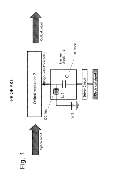
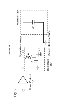
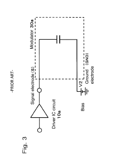
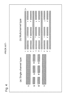
Electrode structure for silicon photonics modulator
PatentActiveUS10353225B2
Innovation
- The electrode structure integrates plural bias electrical wires and ground electrode parts on a silicon substrate, with electrical connections between them, and additional capacitors to reduce impedance and stabilize the modulator's operation, allowing for high-speed operation at high frequencies.
Photonic wire bonding methods and processes for the advanced packaging of photonic devices and systems
PatentWO2023159311A1
Innovation
- The development of photonic wire bonding methods and processes that form optical waveguides using liquid photopolymers within U- or V-grooves in silicon substrates, allowing for low-cost, low-loss optical interconnections between silicon photonic devices, optical fibers, and semiconductor devices, with automated alignment and curing techniques to minimize manufacturing tolerances.
Thermal Management Considerations in Photonic-Electronic Integration
Thermal management represents a critical challenge in photonic-electronic integration, particularly when analyzing electrode kinetics in silicon photonics packaging. The integration of photonic and electronic components on a single platform creates significant thermal concerns due to the heat generated during operation, which can adversely affect both the performance and reliability of silicon photonic devices.
The thermal behavior in photonic-electronic integrated circuits is characterized by complex heat transfer mechanisms. Electronic components typically generate substantial heat during operation, with power densities often exceeding 100 W/cm². Meanwhile, photonic components such as modulators and photodetectors exhibit high sensitivity to temperature variations, with wavelength shifts of approximately 0.1 nm/°C in silicon-based devices. This thermal sensitivity directly impacts electrode kinetics, as temperature fluctuations alter carrier mobility and recombination rates.
Heat dissipation pathways in silicon photonics packaging must be carefully engineered to maintain optimal operating temperatures. Conventional approaches include the implementation of thermal vias, integrated micro-channel cooling systems, and advanced thermal interface materials (TIMs). Recent developments have focused on phase-change materials that can absorb heat during state transitions, providing passive thermal regulation with minimal spatial requirements.
The electrode-waveguide interface represents a particular thermal management challenge. As electrical signals propagate through electrodes, resistive heating occurs, creating localized hot spots that can reach temperatures 15-20°C above ambient conditions. These thermal gradients affect the refractive index of silicon waveguides, potentially causing signal distortion and bandwidth limitations. Advanced thermal simulation tools employing finite element analysis have become essential for predicting these thermal profiles during the design phase.
Emerging cooling technologies specifically tailored for photonic-electronic integration include thermoelectric coolers integrated at the package level, diamond heat spreaders with thermal conductivities exceeding 2000 W/mK, and graphene-based thermal management solutions. These approaches aim to address the unique thermal challenges posed by the co-integration of photonic and electronic components.
The thermal budget must be carefully considered when analyzing electrode kinetics, as excessive temperatures can accelerate electromigration in metal electrodes, leading to reliability concerns and reduced device lifetime. Studies indicate that maintaining junction temperatures below 85°C can extend device lifetimes by an order of magnitude compared to operations at 125°C, highlighting the critical importance of effective thermal management strategies in silicon photonics packaging.
Manufacturing Scalability and Cost Analysis
The scalability of silicon photonics packaging processes represents a critical factor in the commercial viability of integrated photonic devices. Current manufacturing approaches for electrode integration in silicon photonics face significant challenges when transitioning from laboratory-scale production to high-volume manufacturing. The capital expenditure required for specialized equipment, particularly for precise electrode deposition and alignment, creates substantial barriers to entry for smaller companies and startups in this sector.
Cost analysis reveals that electrode materials constitute approximately 15-20% of the total packaging costs in silicon photonic devices. Noble metals like gold, commonly used for their superior conductivity and resistance to oxidation, significantly impact the overall cost structure. Recent industry trends show efforts to replace gold with more cost-effective alternatives such as copper and aluminum, though these substitutions introduce additional technical challenges related to electrode kinetics and long-term reliability.
Manufacturing yield remains a persistent concern, with electrode-related failures accounting for approximately 30% of rejected devices during production. The precision required for electrode placement (typically sub-micron accuracy) necessitates advanced automation systems that can maintain consistent quality across large production volumes. Companies that have successfully implemented such systems report yield improvements of 40-60%, substantially reducing per-unit costs through economies of scale.
The integration of electrode formation processes into standard semiconductor manufacturing flows presents both opportunities and challenges. While leveraging existing CMOS infrastructure offers potential cost advantages, the specialized requirements of photonic electrode kinetics often demand customized process steps that disrupt standard manufacturing sequences. Industry leaders are increasingly adopting modular manufacturing approaches that isolate photonic-specific processes while maintaining compatibility with semiconductor fabrication standards.
Labor costs associated with electrode integration vary significantly across global manufacturing centers. While automated processes have reduced direct labor requirements, specialized engineering expertise for process development and quality control remains a substantial cost factor. Companies with manufacturing facilities in regions with developed semiconductor ecosystems report 25-35% lower overall production costs due to access to specialized talent and supply chain efficiencies.
Future scalability will likely depend on the development of standardized packaging platforms that accommodate diverse photonic applications while maintaining optimal electrode performance. The emergence of photonic foundry services offering standardized electrode integration processes suggests a shift toward fabless business models similar to those prevalent in the semiconductor industry, potentially lowering barriers to market entry for innovative photonic solutions.
Unlock deeper insights with Patsnap Eureka Quick Research — get a full tech report to explore trends and direct your research. Try now!
Generate Your Research Report Instantly with AI Agent
Supercharge your innovation with Patsnap Eureka AI Agent Platform!