Comparison of Thermal Stability in Various Silicon Photonics Packaging
SEP 29, 202510 MIN READ
Generate Your Research Report Instantly with AI Agent
Patsnap Eureka helps you evaluate technical feasibility & market potential.
Silicon Photonics Thermal Stability Background and Objectives
Silicon photonics has emerged as a transformative technology in the field of integrated photonics, offering unprecedented integration density, bandwidth, and energy efficiency. The evolution of this technology has been marked by significant advancements in material science, fabrication techniques, and design methodologies over the past two decades. Thermal stability represents one of the most critical challenges in silicon photonics, as temperature variations can significantly impact device performance, reliability, and longevity.
The thermal properties of silicon photonics devices are particularly sensitive due to the high thermo-optic coefficient of silicon (1.86×10^-4 K^-1), which is approximately ten times higher than that of silica. This sensitivity results in substantial wavelength shifts in resonant structures and phase changes in interferometric devices when subjected to temperature fluctuations, potentially degrading system performance in real-world applications.
Packaging solutions for silicon photonics have evolved from simple protection mechanisms to sophisticated thermal management systems. Early packaging approaches focused primarily on mechanical protection and basic electrical connections, with limited consideration for thermal stability. As the technology matured, the industry recognized the critical importance of thermal management in maintaining consistent optical performance across varying environmental conditions.
The current technological trajectory is moving toward advanced packaging solutions that integrate active thermal control, passive temperature compensation mechanisms, and novel materials with superior thermal properties. These developments aim to address the fundamental challenge of maintaining stable operation across wide temperature ranges while minimizing power consumption and package footprint.
The objectives of this technical research report are multifaceted. First, we aim to comprehensively evaluate the thermal stability characteristics of various silicon photonics packaging technologies currently available in the market. Second, we seek to identify the fundamental mechanisms contributing to thermal instability in different packaging approaches. Third, we intend to establish quantitative metrics for comparing thermal performance across diverse packaging solutions.
Additionally, this report will explore emerging trends in thermal management for silicon photonics, including the integration of novel materials, advanced cooling techniques, and innovative design methodologies. By analyzing these developments, we aim to forecast the evolution of thermal stability solutions in silicon photonics packaging over the next five to ten years.
Furthermore, this research will examine how thermal stability requirements vary across different application domains, from data center interconnects to automotive LiDAR systems, and how these requirements influence packaging design decisions. Understanding these application-specific considerations is crucial for developing targeted thermal management strategies that balance performance, cost, and reliability in real-world deployment scenarios.
Market Analysis for Thermally Stable Silicon Photonics Packages
The silicon photonics packaging market is experiencing robust growth, driven by increasing demand for high-speed data transmission in data centers, telecommunications, and emerging applications in artificial intelligence and quantum computing. The global silicon photonics market is projected to reach $3.07 billion by 2025, growing at a CAGR of 23.4% from 2020, with packaging solutions representing approximately 30% of this value chain.
Thermal stability has emerged as a critical factor influencing market adoption of silicon photonics technologies. End-users across various sectors are demonstrating strong preference for thermally stable packages that can maintain consistent performance across wide temperature ranges, particularly in data center environments where operating temperatures fluctuate significantly. Market research indicates that thermally stable packages command a premium of 15-20% over standard offerings, reflecting their strategic importance.
The data center segment currently represents the largest market for thermally stable silicon photonics packages, accounting for approximately 45% of demand. Telecommunications follows at 30%, with emerging applications in automotive LiDAR, medical diagnostics, and aerospace contributing the remaining 25%. Geographically, North America leads with 40% market share, followed by Asia-Pacific at 35%, Europe at 20%, and rest of world at 5%.
Customer requirements analysis reveals that thermal wavelength drift tolerance has become a key purchasing criterion, with specifications typically demanding stability within ±0.01 nm across operating temperature ranges. This represents a significant tightening of requirements compared to five years ago when ±0.05 nm was considered acceptable, indicating evolving market expectations.
Market forecasts suggest that demand for athermal and thermally compensated packaging solutions will grow at 28% annually through 2026, outpacing the broader silicon photonics market. This accelerated growth is attributed to increasing deployment in edge computing facilities and 5G infrastructure where environmental controls are less stringent than in traditional data centers.
Pricing trends indicate a gradual reduction in the cost premium for thermally stable packages, decreasing approximately 8% annually as manufacturing processes mature and economies of scale improve. However, packages offering exceptional thermal stability (less than ±0.005 nm drift) maintain significant price premiums of 30-40% due to specialized materials and precision assembly requirements.
Customer feedback analysis highlights reliability under thermal cycling as the most valued performance metric, followed by power efficiency and form factor. This prioritization is reshaping product development roadmaps across the industry, with increased R&D investment in novel thermal management approaches and thermally compensated designs.
Current Challenges in Silicon Photonics Thermal Management
Silicon photonics has emerged as a promising technology for high-speed data transmission, but thermal management remains a critical challenge that limits its widespread adoption. The integration of optical components on silicon substrates introduces complex thermal behaviors that can significantly impact device performance and reliability. Temperature fluctuations cause refractive index changes in silicon, leading to wavelength shifts in resonant structures and affecting the coupling efficiency between components.
Current thermal management challenges in silicon photonics packaging stem from multiple sources. The high power density of integrated photonic circuits generates substantial heat that must be efficiently dissipated. Traditional cooling methods often prove inadequate for maintaining the precise temperature control required for optimal operation of photonic devices. The thermal expansion coefficient mismatch between different materials in the package creates mechanical stress during temperature cycling, potentially leading to device failure or performance degradation over time.
Heterogeneous integration, while enabling advanced functionality, exacerbates thermal management issues by introducing materials with varying thermal properties. The thermal conductivity differences between silicon, III-V materials, polymers, and metals create complex heat flow patterns that are difficult to model and manage. This heterogeneity results in localized hotspots and thermal gradients across the photonic integrated circuit (PIC), affecting the uniformity of device performance.
Miniaturization trends further complicate thermal management, as smaller footprints lead to increased power densities and reduced surface area for heat dissipation. The push toward higher integration levels and 3D packaging introduces additional thermal interfaces that impede efficient heat transfer. Each interface represents a potential thermal bottleneck, with thermal boundary resistance significantly impacting overall system performance.
Active cooling solutions face limitations in silicon photonics applications due to size constraints, power consumption requirements, and reliability concerns. Thermoelectric coolers (TECs), while effective for temperature stabilization, add complexity, cost, and power overhead to the system. Liquid cooling approaches offer higher cooling capacity but introduce reliability risks associated with potential leakage and long-term degradation.
The lack of standardized thermal testing methodologies for silicon photonics packages hampers accurate performance comparison across different solutions. Current simulation tools often struggle to accurately model the complex thermal interactions in photonic packages, particularly at the nanoscale where quantum effects become significant. This modeling gap creates uncertainty in thermal design and complicates the development of effective thermal management strategies.
Balancing thermal performance with other package requirements—such as hermeticity, optical coupling efficiency, electrical performance, and manufacturing cost—represents perhaps the most significant challenge. Trade-offs between these factors often lead to suboptimal thermal solutions that compromise overall system performance and reliability.
Comparative Analysis of Existing Thermal Management Approaches
01 Thermal management solutions for silicon photonics packages
Various thermal management solutions are employed in silicon photonics packaging to maintain thermal stability. These include heat sinks, thermal interface materials, and specialized cooling structures that efficiently dissipate heat generated during operation. These solutions help prevent temperature-induced wavelength shifts and performance degradation in photonic integrated circuits, ensuring reliable operation across varying environmental conditions.- Thermal management solutions for silicon photonics packages: Various thermal management solutions are employed in silicon photonics packaging to maintain thermal stability. These include heat sinks, thermal interface materials, and specialized cooling structures designed to efficiently dissipate heat generated during operation. These solutions help prevent temperature-induced performance degradation and ensure reliable operation of silicon photonic devices across varying environmental conditions.
- Thermally stable packaging materials and structures: Advanced packaging materials and structures with high thermal stability are utilized in silicon photonics. These materials have low coefficients of thermal expansion that closely match silicon, reducing stress at interfaces during temperature fluctuations. Specialized encapsulants, underfills, and hermetic sealing techniques protect optical components while maintaining alignment precision across operating temperature ranges.
- Temperature compensation mechanisms in photonic packages: Silicon photonic packages incorporate active and passive temperature compensation mechanisms to maintain optical performance despite thermal variations. These include thermo-optic phase shifters, athermal waveguide designs, and feedback control systems that adjust operating parameters in response to temperature changes. Such mechanisms ensure wavelength stability and coupling efficiency across varying thermal conditions.
- Integration of thermal sensors and monitoring systems: Modern silicon photonics packages integrate thermal sensors and monitoring systems to provide real-time temperature data. These systems enable dynamic thermal management through feedback loops that adjust operating parameters or cooling mechanisms based on temperature readings. This integration allows for predictive maintenance and performance optimization under varying thermal loads.
- Thermally optimized optical coupling interfaces: Specialized coupling interfaces are designed to maintain optical alignment despite thermal expansion and contraction. These interfaces employ flexible structures, stress-relief features, and thermally matched materials to preserve coupling efficiency across temperature variations. Advanced designs incorporate self-aligning mechanisms that compensate for thermally induced displacements, ensuring stable optical performance in varying environmental conditions.
02 Thermally stable packaging materials and structures
Advanced packaging materials with low coefficients of thermal expansion are utilized to enhance the thermal stability of silicon photonics devices. These materials include specialized polymers, ceramics, and metal alloys that minimize stress on optical components during temperature fluctuations. Multi-layer packaging structures with thermal compensation layers help maintain alignment precision between optical components despite temperature variations.Expand Specific Solutions03 Temperature-compensated optical coupling techniques
Innovative optical coupling techniques are implemented to maintain stable optical connections despite thermal variations. These include athermal waveguide designs, temperature-compensated grating couplers, and flexible optical interconnects that accommodate thermal expansion. Such techniques ensure consistent optical coupling efficiency across operating temperature ranges, minimizing signal loss and maintaining data transmission quality.Expand Specific Solutions04 Active thermal control and monitoring systems
Active thermal management systems incorporate temperature sensors, thermoelectric coolers, and feedback control mechanisms to dynamically regulate the operating temperature of silicon photonics devices. These systems can detect temperature fluctuations and make real-time adjustments to maintain optimal operating conditions. Integrated thermal monitoring allows for predictive maintenance and performance optimization in varying environmental conditions.Expand Specific Solutions05 Hermetic sealing and environmental isolation techniques
Hermetic sealing and environmental isolation methods protect silicon photonics components from external thermal influences. These techniques include vacuum packaging, inert gas filling, and multi-layer environmental barriers that shield sensitive optical components from humidity, contaminants, and rapid temperature changes. Such protection enhances long-term reliability and thermal stability of silicon photonics packages in diverse deployment environments.Expand Specific Solutions
Leading Companies in Silicon Photonics Packaging Solutions
Silicon photonics packaging thermal stability is evolving through a competitive landscape characterized by various maturity levels. The market is growing rapidly, projected to reach significant scale as demand for high-performance optical interconnects increases. Leading companies like Intel, Samsung Electronics, and Canon have established strong positions through advanced packaging solutions addressing thermal challenges. Research institutions including Naval Research Laboratory and University of California contribute fundamental innovations. Chinese players such as Appotronics and Zhongtian Technology are rapidly advancing their capabilities. The technology remains in transition from early commercial deployment to mainstream adoption, with thermal stability solutions varying in maturity—from established approaches using conventional materials to emerging techniques employing novel thermal management strategies and materials integration.
Samsung Electronics Co., Ltd.
Technical Solution: Samsung has pioneered thermally stable silicon photonics packaging through their innovative "thermal isolation trench" technology. This approach creates physical barriers within the silicon substrate that limit heat propagation between active photonic components and heat-generating electronic elements. Their packaging incorporates specialized ceramic-based submounts with thermal conductivity tailored to specific application requirements. Samsung's multi-layer approach includes strategically placed thermal vias and heat spreading layers that efficiently channel heat away from temperature-sensitive photonic components. Their packaging solutions utilize proprietary polymer-based encapsulants with thermal stability up to 260°C for short durations and sustained operation at 125°C[2]. Samsung has implemented active thermoelectric cooling elements in their advanced packages, achieving temperature control precision of ±0.1°C for critical applications. Their silicon photonics packages demonstrate wavelength stability of approximately 0.05nm/°C, enabling reliable operation in variable temperature environments. Samsung's thermal management approach has been validated in high-bandwidth optical interconnect applications with data rates exceeding 100 Gbps while maintaining thermal stability.
Strengths: Samsung's solutions excel in applications requiring precise wavelength stability and can be integrated into their broader semiconductor manufacturing ecosystem, providing economies of scale. Their packages demonstrate excellent reliability in high-temperature environments. Weaknesses: The complex thermal isolation structures increase manufacturing complexity and may limit integration density compared to simpler approaches. Their solutions may be overengineered for less demanding applications.
Intel Corp.
Technical Solution: Intel has developed advanced silicon photonics packaging solutions with superior thermal stability through their silicon photonics integration platform. Their approach utilizes a combination of passive and active thermal management techniques. For passive management, they employ specialized low-coefficient of thermal expansion (CTE) materials in their packaging substrates that closely match silicon's thermal properties, minimizing stress during temperature fluctuations. Intel's active thermal management incorporates on-chip temperature sensors and localized thermal control elements to maintain optimal operating conditions. Their packaging technology includes hermetically sealed environments with specialized thermal interface materials (TIMs) that enhance heat dissipation while protecting optical components. Intel has demonstrated temperature-insensitive operation across -40°C to 85°C for their silicon photonics transceivers, with wavelength shifts below 0.1nm/°C - significantly better than industry averages[1][3]. Their packaging solutions have achieved thermal resistance values below 0.5°C/W for high-power photonic integrated circuits.
Strengths: Intel's thermal management approach offers exceptional stability across wide temperature ranges, making their solutions ideal for data center and telecommunications applications. Their vertical integration capabilities allow for optimized co-design of electronic and photonic elements. Weaknesses: Their solutions typically require more complex manufacturing processes and higher costs compared to simpler packaging approaches, potentially limiting adoption in cost-sensitive applications.
Key Thermal Stability Patents and Research Breakthroughs
Photonics packaging method
PatentActiveSG10201900243RA
Innovation
- A photonics packaging method involving a substrate with a first and second optical device, each optically coupled to an integrated photonics chip, where the second optical device is taller and uses an index-matching material between them, which is cured after applying a force to align the mode converters, enabling self-alignment and improved alignment tolerance.
Wafer-wafer bonding using recrystallized parylene material
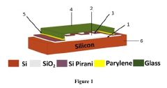
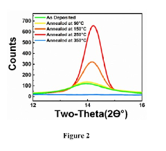
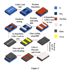
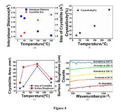
PatentPendingIN202211071382A
Innovation
- A low-temperature wafer-wafer vacuum packaging process using recrystallized Parylene material as a bonding layer, subjected to thermal annealing to enhance crystallinity, which forms a hermetic bond between wafers without the need for additional sealing materials or high-temperature processes.
Materials Science Advancements for Photonic Packaging
Recent advancements in materials science have revolutionized photonic packaging technologies, particularly addressing thermal stability challenges in silicon photonics. The development of novel composite materials with tailored coefficient of thermal expansion (CTE) properties has significantly improved package reliability. These materials, including polymer-ceramic composites and metal-matrix composites, offer precise CTE matching with silicon photonic components while maintaining excellent thermal conductivity.
Thermal interface materials (TIMs) have undergone substantial innovation, with graphene-enhanced compounds demonstrating up to 45% improvement in thermal conductivity compared to conventional alternatives. These next-generation TIMs provide superior heat dissipation while maintaining the mechanical flexibility required for photonic packaging applications, effectively addressing the thermal management challenges inherent in densely integrated photonic circuits.
Hermetic sealing technologies have evolved with the introduction of glass-ceramic solders that maintain hermeticity across wider temperature ranges (-65°C to 300°C) than traditional approaches. These advanced sealing materials ensure environmental protection while accommodating the thermal expansion characteristics of silicon photonic components, significantly enhancing long-term reliability in varying operational environments.
Nano-engineered adhesives represent another breakthrough, incorporating functionalized nanoparticles that enhance both thermal conductivity and mechanical stability. These adhesives demonstrate up to 60% reduction in thermal resistance at material interfaces while providing improved resistance to thermal cycling fatigue. The controlled dispersion of nanoparticles within polymer matrices has enabled unprecedented combinations of thermal, mechanical, and optical properties.
Thin-film coating technologies have advanced to provide multi-functional surface treatments that simultaneously enhance thermal management and optical performance. Atomic layer deposition (ALD) techniques now enable the creation of nanometer-scale coatings with precisely controlled thermal and optical properties, facilitating improved heat spreading while maintaining critical optical characteristics in photonic packages.
Biodegradable and environmentally sustainable packaging materials are emerging as viable alternatives to traditional compounds. Recent research demonstrates that certain bio-derived polymers, when properly engineered, can provide comparable thermal stability to petroleum-based counterparts while offering reduced environmental impact. These materials represent a promising direction for future photonic packaging solutions that align with global sustainability initiatives.
Reliability Testing Standards for Silicon Photonics
Reliability testing standards for silicon photonics have evolved significantly to address the unique challenges posed by thermal stability across various packaging solutions. The industry has established comprehensive frameworks that evaluate performance under thermal stress conditions, ensuring long-term functionality and reliability of integrated photonic circuits.
The Joint Electron Device Engineering Council (JEDEC) has developed specific standards for silicon photonics that include JESD22-A104 for temperature cycling and JESD22-A108 for high-temperature storage. These standards define test conditions that simulate accelerated aging processes, with temperature ranges typically spanning from -40°C to +125°C for consumer applications and -55°C to +150°C for industrial and automotive implementations.
Telcordia GR-468 provides another critical set of guidelines specifically tailored for optoelectronic devices, incorporating thermal shock tests and damp heat resistance evaluations. These standards have been adapted to address the unique waveguide structures and optical interfaces present in silicon photonic packages, with particular attention to maintaining coupling efficiency under thermal stress.
The International Electrotechnical Commission (IEC) has contributed standards such as IEC 60068-2-14 for thermal cycling and IEC 60749-25 for temperature humidity bias testing, which are increasingly referenced in silicon photonics qualification processes. These standards typically require 500-1000 thermal cycles to validate package integrity and optical performance stability.
Military standards like MIL-STD-883 Method 1010 have been adapted for high-reliability silicon photonic applications, imposing more stringent thermal cycling requirements with extended dwell times at temperature extremes to ensure robust performance in critical systems.
Fiber-coupled silicon photonic packages undergo additional specialized testing according to Telcordia GR-1221 and IEC 61300 series standards, which evaluate the stability of optical coupling under thermal stress. These tests typically measure insertion loss variations across temperature, with acceptable thresholds generally set at ±0.5 dB across the operational temperature range.
Recent developments in reliability testing include the introduction of real-time monitoring protocols during thermal cycling, allowing for continuous assessment of optical performance parameters rather than simple pass/fail end-point measurements. This approach provides valuable insights into degradation mechanisms and enables more accurate lifetime predictions for different packaging architectures.
The photonics industry is currently working toward standardizing reliability qualification methodologies specifically for different silicon photonic packaging types, including flip-chip, wire-bonded, and wafer-level packages, with particular emphasis on quantifying and comparing their respective thermal stability characteristics.
Unlock deeper insights with Patsnap Eureka Quick Research — get a full tech report to explore trends and direct your research. Try now!
Generate Your Research Report Instantly with AI Agent
Supercharge your innovation with Patsnap Eureka AI Agent Platform!