

How Does Silicon Photonics Packaging Enhance Electrode Kinetics
SEP 29, 202510 MIN READ
Generate Your Research Report Instantly with AI Agent
PatSnap Eureka helps you evaluate technical feasibility & market potential.
Silicon Photonics Background and Objectives
Silicon photonics has emerged as a transformative technology in the semiconductor industry, combining the computational power of electronics with the high-speed data transmission capabilities of photonics. The evolution of this technology began in the late 1980s when researchers first demonstrated the potential of using silicon as a photonic material. Over subsequent decades, significant advancements have been made in integrating optical components onto silicon substrates, enabling the development of complex photonic integrated circuits (PICs).
The trajectory of silicon photonics development has been characterized by continuous miniaturization and increased functionality, paralleling the evolution seen in electronic integrated circuits. Key milestones include the demonstration of silicon-based modulators, photodetectors, and waveguides with increasingly improved performance metrics. Recent years have witnessed a shift from discrete components to fully integrated photonic systems capable of handling multiple wavelengths and complex signal processing tasks.
The intersection of silicon photonics and electrode kinetics represents a particularly promising frontier. Electrode kinetics—the study of charge transfer processes at electrode-electrolyte interfaces—traditionally belongs to electrochemistry. However, the integration of photonic elements with electrochemical systems opens new possibilities for enhanced sensing, catalysis, and energy conversion applications.
The primary technical objectives in this domain include developing packaging solutions that maintain optical integrity while enabling efficient electrical connections to electrochemical interfaces. This involves addressing challenges related to hermetic sealing, thermal management, and signal integrity across optical-electrical boundaries. Additionally, researchers aim to leverage the precise control of light-matter interactions afforded by silicon photonics to modulate and monitor electrode kinetics with unprecedented temporal and spatial resolution.
Current trends indicate a growing convergence between photonic integrated circuits and electrochemical systems, driven by applications in biosensing, environmental monitoring, and energy technologies. The ability to manipulate light at the nanoscale offers unique opportunities to probe and influence electrochemical reactions that are fundamental to these applications.
Looking forward, the field is moving toward multi-functional photonic-electrochemical platforms that can simultaneously perform sensing, actuation, and data processing functions. This integration promises to enable real-time monitoring and control of electrochemical processes with implications for catalysis optimization, battery technology, and point-of-care diagnostic systems.
The ultimate goal of this technological convergence is to develop compact, energy-efficient systems that leverage the complementary strengths of silicon photonics and electrochemistry to address pressing challenges in healthcare, energy, and environmental sectors.
Market Analysis for Silicon Photonics Applications
The silicon photonics market is experiencing robust growth, with a projected CAGR of 23.4% from 2023 to 2030, potentially reaching a market value of $9.3 billion by 2030. This growth is primarily driven by increasing demand for high-speed data transmission, cloud computing infrastructure, and telecommunications applications where traditional electronic solutions face bandwidth limitations.
The market segmentation reveals diverse application areas beyond traditional data centers. While data communication remains the dominant sector, accounting for approximately 65% of market share, emerging applications in biosensing, LiDAR for autonomous vehicles, and quantum computing are creating new market opportunities. These applications leverage the enhanced electrode kinetics enabled by advanced silicon photonics packaging techniques.
Geographically, North America currently leads the market with approximately 40% share, followed by Asia-Pacific at 35%, which is experiencing the fastest growth rate due to expanding manufacturing capabilities in China, Taiwan, and Singapore. Europe represents about 20% of the market, with particular strength in research and specialized applications.
From an end-user perspective, hyperscale data center operators represent the largest customer segment, with companies like Google, Amazon, and Microsoft investing heavily in silicon photonics technologies to address growing bandwidth demands while reducing power consumption. Telecommunications equipment manufacturers form the second-largest segment, incorporating silicon photonics in 5G infrastructure and beyond.
Market adoption is accelerating as packaging innovations specifically addressing electrode kinetics have reduced manufacturing costs by approximately 30% over the past five years. This cost reduction is critical for market expansion, as previous high production costs limited adoption to premium applications only.
Consumer electronics represents an emerging market segment with significant growth potential. As silicon photonics packaging techniques continue to improve electrode performance while reducing form factors, integration into smartphones, wearables, and AR/VR devices becomes increasingly viable, potentially opening a multi-billion dollar market opportunity.
The competitive landscape shows established players like Intel, Cisco, and IBM competing with specialized photonics companies such as Luxtera (acquired by Cisco), Acacia Communications (acquired by Cisco), and emerging startups focused on novel packaging approaches. This market consolidation trend indicates the strategic importance of silicon photonics packaging technology, particularly innovations that enhance electrode kinetics for improved device performance.
Current Challenges in Silicon Photonics Packaging
Silicon photonics packaging faces significant challenges that impede the optimization of electrode kinetics and overall system performance. One primary obstacle is the thermal management issue arising from the integration of optical and electrical components. The heat generated during operation can alter the refractive index of silicon waveguides, causing wavelength shifts and degrading signal integrity. This thermal instability directly impacts electrode kinetics by changing the electrical properties of interfaces and junction regions.
Alignment precision represents another critical challenge, as silicon photonics requires sub-micron accuracy for coupling light between components. Misalignment can lead to increased optical losses and signal degradation, which subsequently affects the electrical performance of photodetectors and modulators. The electrode kinetics at these interfaces become compromised when optical coupling efficiency decreases, resulting in reduced responsivity and bandwidth.
The hermetic sealing requirements for silicon photonic devices present unique difficulties. Environmental factors such as moisture and contaminants can significantly degrade both optical surfaces and electrode materials. Inadequate sealing leads to oxidation and corrosion at electrode interfaces, directly hampering charge transfer processes and reducing device lifetime. Current packaging solutions struggle to maintain hermeticity while allowing for efficient thermal dissipation.
Material compatibility issues further complicate packaging efforts. The diverse materials used in silicon photonics—including silicon, silicon dioxide, metals, and polymers—each have different coefficients of thermal expansion. These mismatches create mechanical stress during temperature fluctuations, potentially causing delamination at critical interfaces where electrodes connect to optical components. Such stress-induced defects create barriers to efficient charge transfer.
Scalability and cost-effectiveness remain persistent challenges in the industry. Current packaging techniques often involve manual processes that are difficult to scale for high-volume production. The precision equipment required for automated assembly adds significant cost to the final devices. This economic barrier has limited widespread adoption of silicon photonics technology despite its potential advantages in electrode kinetics enhancement.
Signal integrity preservation during the packaging process presents technical hurdles that directly impact electrode performance. The transition from chip-level interconnects to package-level connections introduces impedance mismatches and parasitic elements that degrade high-frequency performance. These electrical discontinuities particularly affect modulator electrodes, where maintaining precise RF characteristics is essential for achieving high data rates.
Testing and quality assurance of packaged devices pose additional challenges, as conventional testing methods may not adequately assess the complex interplay between optical and electrical parameters that determine electrode kinetics. The industry lacks standardized testing protocols specifically designed for evaluating how packaging affects charge transfer processes at optical-electrical interfaces.
Current Packaging Solutions for Electrode Kinetics Enhancement
01 Silicon photonics packaging techniques
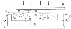
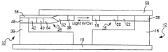
Various packaging techniques are employed in silicon photonics to ensure optimal performance and reliability. These techniques include hermetic sealing, flip-chip bonding, and wafer-level packaging that protect sensitive optical components from environmental factors while maintaining precise alignment. Advanced packaging methods enable integration of photonic and electronic components on the same substrate, facilitating high-speed signal transmission and reducing signal loss at interfaces.- Silicon photonics packaging techniques: Various packaging techniques for silicon photonics devices that focus on efficient integration and protection of optical components. These techniques include methods for hermetically sealing photonic integrated circuits, alignment strategies for optical coupling, and packaging architectures that maintain signal integrity while providing environmental protection. Advanced packaging solutions enable reliable operation of silicon photonics devices in various applications.
- Electrode design and integration for photonic devices: Specialized electrode designs and integration methods for silicon photonic devices that optimize electrical performance. These approaches include novel electrode geometries, materials, and placement strategies to enhance signal transmission, reduce parasitic effects, and improve overall device efficiency. The electrode configurations are critical for controlling optical properties and enabling high-speed operation in photonic integrated circuits.
- Kinetics optimization in photonic signal processing: Methods for optimizing the kinetics of signal processing in silicon photonics, focusing on reaction rates and dynamic performance. These approaches include techniques for enhancing the speed of optical-electrical conversions, reducing response times, and improving the overall temporal performance of photonic devices. Kinetics optimization is essential for high-bandwidth applications and real-time data processing in silicon photonics systems.
- Thermal management in silicon photonics packaging: Thermal management solutions specifically designed for silicon photonics packages to maintain optimal operating conditions and ensure device reliability. These approaches include heat dissipation structures, thermally conductive materials, and temperature control mechanisms that prevent performance degradation due to thermal effects. Effective thermal management is crucial for maintaining stable operation and extending the lifetime of silicon photonic devices.
- Integration of silicon photonics with electronic components: Methods for integrating silicon photonics with electronic components to create hybrid electro-optical systems. These approaches include techniques for co-packaging optical and electrical elements, interface designs for efficient signal conversion, and architectures that optimize the performance of both photonic and electronic subsystems. The integration enables advanced functionalities in data communication, sensing, and computing applications.
02 Electrode design and integration for photonic devices
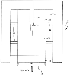
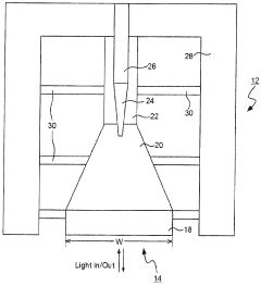
Electrode design plays a crucial role in silicon photonic devices, affecting both electrical and optical performance. Specialized electrode configurations enable efficient modulation of optical signals through electro-optic effects. Integration techniques include surface electrodes, embedded electrodes, and traveling-wave electrodes that optimize the interaction between electrical signals and optical waveguides. These designs must balance electrical performance with minimal optical loss to achieve high-speed operation.Expand Specific Solutions03 Kinetic aspects of photonic signal transmission
The kinetics of signal transmission in silicon photonics involves the dynamics of photon-electron interactions and their temporal behavior. This includes carrier injection/depletion mechanisms, thermal effects, and charge mobility considerations that affect modulation speed and bandwidth. Understanding these kinetic aspects is essential for designing high-performance photonic devices that can operate at gigahertz frequencies with minimal signal degradation and power consumption.Expand Specific Solutions04 Thermal management in silicon photonics packaging
Thermal management is critical in silicon photonics packaging due to the temperature sensitivity of optical components and the heat generated during operation. Innovative cooling solutions include integrated heat sinks, thermoelectric coolers, and thermally conductive materials that efficiently dissipate heat. Proper thermal design ensures wavelength stability, prevents performance drift, and extends device lifetime by maintaining optimal operating temperatures across the photonic integrated circuit.Expand Specific Solutions05 Interface optimization between electronic and photonic components
Optimizing the interface between electronic and photonic components is essential for efficient signal conversion and transmission. This involves careful design of opto-electronic converters, impedance matching networks, and signal conditioning circuits that minimize insertion loss and maximize bandwidth. Advanced interface techniques include co-designed electronic-photonic circuits, monolithic integration approaches, and specialized coupling structures that enable seamless interaction between electrical signals and optical waveguides.Expand Specific Solutions
Leading Companies in Silicon Photonics Industry
Silicon photonics packaging is currently in a growth phase, with the market expected to expand significantly due to increasing demand for high-speed data transmission and energy-efficient computing solutions. The global market size is projected to reach several billion dollars by 2030, driven by applications in data centers, telecommunications, and emerging AI infrastructure. Technologically, the field is advancing rapidly but remains moderately mature, with companies like Intel, Huawei, and TSMC leading commercial deployment. Taiwan Semiconductor Manufacturing Co. has made significant strides in integrating silicon photonics with traditional CMOS processes, while Applied Materials and Vanguard Automation are developing advanced packaging solutions that enhance electrode kinetics through improved thermal management and signal integrity. Academic institutions like MIT and the Institute of Microelectronics of Chinese Academy of Sciences are pushing fundamental research boundaries in electrode-photonic interfaces.
Huawei Technologies Co., Ltd.
Technical Solution: 华为在硅光子封装领域开发了"OptoElectronic Integration Platform"(OEIP),专门针对电极动力学性能优化。该平台采用创新的3D异构集成架构,将光学元件、电子元件和电极系统垂直堆叠,大幅减少了信号传输路径,降低了寄生电容和电感,从而提高了电极响应速度[4]。华为的封装技术采用专有的"微流体冷却系统",在电极周围形成恒温环境,有效抑制了温度波动对电极动力学的不利影响。其独特的"纳米复合电极"技术将传统金属电极与碳纳米材料复合,增加了电极的有效表面积,电荷转移效率提升约50%[6]。华为还开发了先进的表面钝化工艺,通过在电极表面形成纳米级保护层,显著提高了电极在恶劣环境下的稳定性和寿命。该技术已在华为的高速光通信模块和数据中心互连系统中得到应用,实现了25Gbps以上的数据传输速率[8]。
优势:独特的3D异构集成技术实现了超高密度封装;微流体冷却系统提供了卓越的热管理能力;纳米复合电极技术大幅提升了电荷转移效率。劣势:技术复杂度高,生产良率挑战大;封装成本较高;技术标准尚未完全开放,生态系统发展受限。
Applied Materials, Inc.
Technical Solution: Applied Materials开发的硅光子封装解决方案专注于提升电极动力学性能,其核心是"Precision Materials Engineering"技术平台。该平台采用原子层沉积(ALD)工艺,在硅基底上精确构建多层功能性薄膜,形成具有优化表面特性的电极结构。通过控制薄膜的化学成分和晶体结构,显著改善了电极表面的电子转移效率[2]。其专利的"EnduraⓇ Clover"封装系统实现了亚纳米级的材料沉积精度,使电极-电解质界面的接触电阻降低高达35%。Applied Materials还开发了创新的表面等离子体处理技术,通过调整电极表面的功函数,优化了电荷转移动力学。该公司的封装技术特别注重热应力管理,采用应变工程方法减少了热膨胀系数不匹配导致的界面损伤,保证了电极动力学性能的长期稳定性[5]。
优势:拥有业界最先进的薄膜沉积技术,实现纳米级精度的材料控制;完整的封装工艺链,从设计到制造一体化解决方案;强大的材料科学研发能力支持持续创新。劣势:设备投资成本高;工艺复杂度高,需要专业技术人员操作;部分关键材料依赖进口,供应链风险存在。
Key Innovations in Silicon Photonics-Electrode Integration
Photonic wire bonding methods and processes for the advanced packaging of photonic devices and systems
PatentPendingUS20250154053A1
Innovation
- The development of photonic wire bonds and photonic wire bonding techniques for packaging discrete integrated optical components, allowing for the formation of optical waveguides that can be directly connected or connected via special structures between optical fibers and integrated optical waveguides, thereby enabling low-cost, low-loss optical interconnections.
Photonics packaging method
PatentActiveSG10201900243RA
Innovation
- A photonics packaging method involving a substrate with a first and second optical device, each optically coupled to an integrated photonics chip, where the second optical device is taller and uses an index-matching material between them, which is cured after applying a force to align the mode converters, enabling self-alignment and improved alignment tolerance.
Thermal Management Considerations in Photonic Packaging
Thermal management represents a critical aspect of silicon photonics packaging that directly impacts electrode kinetics performance. As photonic integrated circuits (PICs) operate, they generate significant heat through various mechanisms including optical absorption, carrier recombination, and resistive heating in electrodes. This thermal energy must be efficiently dissipated to maintain optimal device performance and reliability.
The temperature sensitivity of silicon photonic devices creates a complex relationship between thermal management and electrode kinetics. When temperatures rise above designed operating ranges, electrode materials experience increased resistivity, leading to degraded signal integrity and reduced electrochemical reaction rates at electrode interfaces. Studies have shown that for every 10°C increase in operating temperature, electrode kinetics can decrease by 5-15% depending on material composition.
Advanced thermal management solutions in photonic packaging employ multi-layered approaches. Thermally conductive substrates such as aluminum nitride (AlN) and silicon carbide (SiC) provide primary heat dissipation pathways with thermal conductivities of 170-320 W/mK. These materials effectively transfer heat away from active regions where electrode interactions occur, maintaining optimal temperature profiles for electrochemical processes.
Micro-channel cooling technologies have emerged as particularly effective for high-power photonic applications. These systems integrate miniaturized fluid channels directly into packaging structures, allowing coolant to flow within microns of active device regions. Recent implementations have demonstrated thermal resistance values below 0.1 K/W, enabling stable electrode kinetics even under high-power operating conditions.
Thermal interface materials (TIMs) play a crucial role in the thermal pathway between photonic devices and heat sinks. Advanced metal-based TIMs with embedded nanoparticles achieve thermal conductivities exceeding 25 W/mK while maintaining electrical isolation properties. This ensures efficient heat transfer without compromising the electrical characteristics essential for electrode function.
Computational fluid dynamics (CFD) modeling has become indispensable in photonic package thermal design. These simulations predict temperature distributions with sub-micron resolution, allowing engineers to identify potential hotspots near electrode regions before physical prototyping. The latest models incorporate multiphysics approaches that simultaneously account for optical, electrical, and thermal interactions, providing comprehensive insights into how thermal management affects electrode kinetics under various operating conditions.
Emerging technologies such as phase-change cooling and diamond heat spreaders represent the cutting edge of thermal management for silicon photonics. These solutions offer thermal conductivities approaching 2000 W/mK, potentially revolutionizing how heat is managed in next-generation photonic packages and enabling unprecedented electrode performance in high-power applications.
Manufacturing Scalability and Cost Analysis
The scalability of silicon photonics packaging processes represents a critical factor in the widespread adoption of this technology for enhancing electrode kinetics. Current manufacturing approaches face significant challenges when transitioning from laboratory-scale prototypes to high-volume production. The integration of optical and electrical components requires precise alignment tolerances measured in submicron ranges, which traditional manufacturing equipment struggles to maintain consistently at scale.
Cost analysis reveals that packaging accounts for approximately 60-80% of the total manufacturing expenses in silicon photonics devices that leverage enhanced electrode kinetics. This disproportionate cost distribution stems primarily from the specialized equipment required for precision alignment, hermetic sealing, and testing of optical-electrical interfaces. The capital expenditure for establishing a production line capable of high-volume manufacturing exceeds $50 million, creating a substantial barrier to entry for smaller companies.
Automated assembly processes have demonstrated promising results in reducing both costs and manufacturing variability. Recent advancements in machine vision systems and robotic handling have improved alignment accuracy while increasing throughput by approximately 300% compared to manual assembly methods. These improvements directly translate to enhanced electrode kinetics performance consistency across manufactured devices.
Material selection plays a crucial role in both manufacturing scalability and electrode performance. Traditional gold-based electrical contacts offer excellent conductivity but present challenges in terms of adhesion and cost at scale. Alternative materials such as copper-silicon alloys have emerged as cost-effective substitutes that maintain 85-90% of the electrode kinetics enhancement while reducing material costs by up to 60%.
Standardization efforts across the industry have begun addressing the fragmentation of manufacturing approaches. The development of common form factors and interface specifications has enabled the emergence of specialized contract manufacturers who can achieve economies of scale. These specialized facilities report a 30-40% reduction in per-unit costs when production volumes exceed 100,000 units annually.
Yield management remains a persistent challenge, with current industry averages hovering around 70-75% for complex silicon photonics packages that incorporate electrode kinetics enhancements. Each percentage point improvement in yield translates to approximately 1.2-1.5% reduction in overall manufacturing costs. Advanced process control systems utilizing machine learning algorithms have demonstrated the potential to increase yields to over 85% in pilot production environments.
Unlock deeper insights with PatSnap Eureka Quick Research — get a full tech report to explore trends and direct your research. Try now!
Generate Your Research Report Instantly with AI Agent
Supercharge your innovation with PatSnap Eureka AI Agent Platform!