

Silicon Photonics Packaging: Regulatory Challenges and Solutions
SEP 29, 202510 MIN READ
Generate Your Research Report Instantly with AI Agent
PatSnap Eureka helps you evaluate technical feasibility & market potential.
Silicon Photonics Background and Objectives
Silicon photonics has emerged as a transformative technology at the intersection of semiconductor manufacturing and optical communications. Since its conceptual introduction in the late 1980s, silicon photonics has evolved from laboratory experiments to commercial deployment, leveraging the mature CMOS fabrication infrastructure to integrate optical components on silicon substrates. This convergence enables the transmission and processing of light signals within silicon-based integrated circuits, offering unprecedented bandwidth, energy efficiency, and miniaturization capabilities.
The evolution of silicon photonics has been marked by significant milestones, including the development of efficient silicon modulators in the early 2000s, the integration of germanium photodetectors, and more recently, the advancement of hybrid integration techniques incorporating III-V materials for light sources. These developments have collectively addressed the fundamental challenges of generating, modulating, and detecting light in silicon-based platforms.
Current technological trends in silicon photonics are focused on increasing integration density, improving coupling efficiency between optical fibers and photonic chips, enhancing wavelength division multiplexing capabilities, and reducing power consumption. The industry is witnessing a shift from discrete photonic components to fully integrated photonic circuits that can handle multiple optical functions simultaneously.
The packaging of silicon photonic devices represents a critical juncture in the technology's evolution. As photonic integrated circuits (PICs) become more complex and application-specific, packaging solutions must address the precise alignment requirements between optical components, thermal management challenges, and the need for standardized interfaces that comply with regulatory frameworks across different jurisdictions.
The primary objectives of silicon photonics packaging technology development include establishing standardized packaging methodologies that ensure consistent performance, developing cost-effective assembly techniques suitable for high-volume manufacturing, creating reliable testing protocols that validate compliance with regulatory requirements, and designing packaging solutions that maintain signal integrity across diverse environmental conditions.
Additionally, there is a growing emphasis on addressing the regulatory challenges associated with silicon photonics packaging. These include navigating the complex landscape of international standards for optical communication systems, ensuring compliance with electromagnetic compatibility regulations, meeting safety requirements for laser-based systems, and developing environmentally sustainable packaging solutions that align with global initiatives for electronic waste reduction.
The ultimate goal is to establish a robust ecosystem for silicon photonics packaging that balances technological innovation with regulatory compliance, enabling the widespread adoption of this technology across data centers, telecommunications networks, sensing applications, and emerging fields such as quantum computing and artificial intelligence accelerators.
Market Analysis for Silicon Photonics
The silicon photonics market has experienced remarkable growth in recent years, driven primarily by increasing data center demands and telecommunications infrastructure expansion. Current market valuations place the global silicon photonics sector at approximately 2.5 billion USD in 2023, with projections indicating a compound annual growth rate (CAGR) of 23% through 2030, potentially reaching 10.6 billion USD by the end of the decade.
Data centers represent the largest application segment, accounting for roughly 60% of market demand. This dominance stems from silicon photonics' ability to provide high-bandwidth, energy-efficient interconnects crucial for hyperscale computing environments. Telecommunications follows as the second-largest segment at 25%, with emerging applications in sensing, LiDAR, and quantum computing collectively comprising the remaining 15%.
Geographically, North America leads market consumption with 45% market share, followed by Asia-Pacific at 30%, Europe at 20%, and other regions at 5%. However, the Asia-Pacific region demonstrates the fastest growth trajectory, particularly in manufacturing capacity, with China, Taiwan, and Singapore making substantial investments in silicon photonics infrastructure.
The regulatory landscape significantly impacts market dynamics, particularly regarding packaging technologies. Export controls on advanced semiconductor technologies have created supply chain complexities, especially for multinational corporations operating across multiple jurisdictions. These regulatory challenges have accelerated regionalization trends, with companies developing parallel supply chains to ensure compliance with varying national security requirements.
Packaging solutions face particularly stringent regulatory oversight due to their dual-use potential. High-precision alignment technologies used in silicon photonics packaging often fall under export control regimes, creating market access barriers and compliance costs that smaller market entrants struggle to overcome.
Customer demand patterns reveal increasing preference for standardized packaging solutions that simplify regulatory compliance. This has created market opportunities for specialized firms offering "regulation-ready" packaging platforms that incorporate compliance features by design, commanding premium pricing of 15-20% above standard offerings.
The competitive landscape features both established semiconductor giants and specialized photonics firms. Intel, Global Foundries, and AIM Photonics dominate the integrated manufacturing segment, while specialized packaging solution providers like PLC Connections, Teramount, and Luxtera (now Cisco) focus on addressing specific regulatory compliance challenges through innovative coupling and encapsulation technologies.
Technical Challenges in Photonic Packaging
Photonic packaging represents one of the most critical and challenging aspects in the commercialization of silicon photonics technology. The integration of optical components with electronic systems demands precision at the submicron level, creating significant technical hurdles. Current packaging processes face multiple challenges related to optical coupling, thermal management, and hermetic sealing that collectively impact device performance and reliability.
Optical coupling efficiency remains a primary concern in photonic packaging. The fundamental mismatch between the mode size of optical fibers (typically 8-10 μm) and silicon waveguides (approximately 0.5 μm) creates inherent coupling losses that can exceed 20 dB without proper interface solutions. This challenge is further complicated by the need for precise alignment tolerances of less than 0.1 μm in multiple axes, which exceeds the capabilities of many conventional packaging technologies.
Thermal management presents another significant obstacle. Silicon photonic devices are highly temperature-sensitive, with wavelength shifts of approximately 0.1 nm/°C common in resonant structures. This thermal sensitivity necessitates either precise temperature control systems or athermal design approaches, both adding complexity to packaging solutions. The heat generated by co-packaged electronics further exacerbates this issue, creating thermal gradients that can degrade optical performance.
The requirement for hermetic sealing introduces additional complications. Photonic components must be protected from environmental factors such as moisture and contaminants that can degrade performance over time. Traditional hermetic packaging techniques often involve high-temperature processes that can induce stress and misalignment in delicate photonic structures, necessitating the development of specialized low-temperature sealing methods.
Manufacturing scalability represents perhaps the most significant barrier to widespread adoption. Current photonic packaging approaches often rely on active alignment processes that are inherently time-consuming and equipment-intensive. These processes can account for up to 80% of the total device cost, making high-volume production economically challenging. The industry lacks standardized packaging platforms comparable to those in the electronic semiconductor industry, resulting in custom solutions that impede economies of scale.
Material compatibility issues further complicate packaging efforts. The coefficient of thermal expansion (CTE) mismatch between silicon, glass fibers, and packaging materials can induce stress during temperature cycling, leading to alignment shifts and performance degradation. This necessitates careful material selection and design strategies to minimize thermomechanical stress effects.
Testing and quality assurance of packaged photonic devices present unique challenges. Unlike electronic components, optical performance parameters such as insertion loss, polarization-dependent loss, and wavelength accuracy must be measured with high precision. The development of efficient, non-destructive testing methodologies for packaged devices remains an ongoing challenge for manufacturing environments.
Current Packaging Solutions
01 Regulatory compliance for silicon photonics packaging
Silicon photonics packaging must comply with various regulatory standards to ensure safety and performance. These regulations address thermal management, electromagnetic interference, and environmental impact. Manufacturers must navigate complex certification processes across different jurisdictions, particularly for applications in telecommunications and data centers where strict compliance with international standards is required.- Regulatory compliance for silicon photonics packaging: Silicon photonics packaging must comply with various regulatory standards and requirements, including environmental regulations, safety standards, and electromagnetic compatibility. These regulations vary across different regions and countries, creating challenges for manufacturers in ensuring global compliance. Regulatory bodies may require specific testing, certification, and documentation for silicon photonic devices, particularly for applications in telecommunications, data centers, and medical devices.
- Thermal management and reliability challenges: Silicon photonics packaging faces significant thermal management challenges due to the heat generated during operation. Regulatory requirements often specify thermal performance standards and reliability testing protocols to ensure long-term stability and safety. Packaging solutions must address heat dissipation while maintaining optical alignment and performance. Thermal cycling tests and reliability demonstrations are typically required to meet regulatory standards, particularly for high-power applications and devices intended for harsh environments.
- Integration and standardization issues: The lack of standardized packaging approaches for silicon photonics creates regulatory challenges. Different packaging technologies and integration methods may require separate regulatory approvals. Standardization efforts are ongoing but still evolving, making compliance with diverse requirements difficult. Regulatory frameworks often lag behind technological advancements in this rapidly developing field, creating uncertainty for manufacturers. The integration of electronic and photonic components in the same package further complicates regulatory compliance due to the need to meet standards for both technologies.
- Materials and environmental compliance: Silicon photonics packaging must address environmental regulations regarding hazardous materials, recyclability, and end-of-life disposal. Regulations such as RoHS and REACH restrict the use of certain substances in electronic and photonic components. Manufacturers must carefully select packaging materials that meet both technical requirements and environmental regulations. Documentation of material composition and environmental impact assessments may be required for regulatory approval. The use of novel materials in advanced packaging solutions often requires additional regulatory scrutiny.
- Testing and certification protocols: Regulatory challenges include establishing appropriate testing and certification protocols for silicon photonics packages. Traditional electronic testing methods may not adequately address the optical performance aspects of these devices. Specialized testing equipment and procedures are needed to verify compliance with optical, electrical, and mechanical specifications. Certification processes can be time-consuming and costly, particularly for novel packaging approaches without established standards. International harmonization of testing requirements remains a significant challenge for global deployment of silicon photonics technology.
02 Hermetic sealing and environmental protection challenges
Hermetic sealing presents significant regulatory challenges in silicon photonics packaging, as it must protect sensitive optical components from moisture, dust, and other environmental factors. Packaging solutions must meet stringent hermeticity standards while maintaining optical alignment and performance. The materials used must comply with environmental regulations regarding hazardous substances, particularly for applications in medical devices and aerospace.Expand Specific Solutions03 Optical coupling and alignment regulatory requirements
Regulatory requirements for optical coupling and alignment in silicon photonics packaging focus on ensuring consistent performance and reliability. These requirements address precision alignment tolerances, stability over temperature variations, and long-term reliability. Manufacturers must demonstrate compliance with standards for coupling efficiency, insertion loss, and return loss, particularly for telecommunications applications where signal integrity is critical.Expand Specific Solutions04 Thermal management compliance in high-density applications
Thermal management in silicon photonics packaging must comply with regulatory standards for heat dissipation and temperature control. As photonic integrated circuits become more densely packed, thermal challenges increase, requiring innovative cooling solutions that meet safety standards. Regulatory frameworks address maximum operating temperatures, thermal cycling reliability, and heat dissipation efficiency, particularly for data center applications where energy efficiency regulations apply.Expand Specific Solutions05 Integration with electronic components and EMI regulations
The integration of silicon photonics with electronic components presents regulatory challenges related to electromagnetic interference (EMI) and compatibility. Packaging solutions must comply with EMI shielding requirements while maintaining optical performance. Regulations address signal integrity, crosstalk prevention, and electromagnetic compatibility across various applications. This is particularly challenging for high-speed data transmission systems where both optical and electrical performance must meet strict regulatory standards.Expand Specific Solutions
Key Industry Players and Ecosystem
Silicon photonics packaging is evolving in a rapidly growing market, currently transitioning from early commercialization to broader adoption. The market is projected to expand significantly as data centers and telecommunications demand higher bandwidth solutions. Technologically, the field shows varying maturity levels across players. Intel leads with established manufacturing capabilities and integration expertise, while TSMC and GlobalFoundries provide advanced foundry services. Emerging specialists like Ayar Labs and EFFECT Photonics are driving innovation in optical I/O solutions. Huawei and IBM are advancing research in integrated photonics platforms. Academic-industry partnerships involving institutions like Rutgers and Huazhong University are addressing regulatory challenges through standardization efforts and novel packaging approaches that balance performance requirements with compliance demands.
Intel Corp.
Technical Solution: Intel's silicon photonics packaging approach integrates optical components directly with CMOS electronics using their advanced silicon manufacturing processes. Their solution addresses regulatory challenges through a comprehensive design that includes hermetic sealing techniques to protect sensitive optical components from environmental factors. Intel has developed specialized automated assembly processes that maintain precise optical alignment during thermal cycling, a critical requirement for meeting telecommunications reliability standards. Their packaging technology supports data rates exceeding 400 Gbps per fiber while maintaining compliance with industry standards such as Telcordia GR-468 for optoelectronic device reliability. Intel's approach also incorporates built-in self-test capabilities that enable continuous monitoring of optical performance parameters, facilitating compliance with evolving regulatory requirements for telecommunications equipment. The company has successfully deployed their silicon photonics technology in data centers worldwide, demonstrating field reliability that meets or exceeds regulatory expectations.
Strengths: Intel leverages extensive semiconductor manufacturing expertise and infrastructure to achieve high-volume, standardized production capabilities. Their vertical integration from design to fabrication enables better quality control and regulatory compliance management. Weaknesses: Their solutions may have higher initial costs compared to discrete optical components, and the proprietary nature of some technologies may limit interoperability with other vendors' systems.
Huawei Technologies Co., Ltd.
Technical Solution: Huawei has developed a comprehensive silicon photonics packaging platform that addresses regulatory challenges through multiple innovative approaches. Their solution incorporates advanced hermetic sealing technologies that protect sensitive optical components while meeting international standards for telecommunications equipment reliability. Huawei's packaging technology utilizes automated precision alignment systems that maintain optical coupling efficiency within 0.1dB variation across operating temperature ranges, satisfying stringent performance requirements of regulatory bodies worldwide. Their approach includes specialized thermal management structures that dissipate heat effectively while maintaining the integrity of optical interfaces, a critical factor for meeting safety regulations. Huawei has implemented comprehensive testing protocols that verify compliance with electromagnetic compatibility standards, ensuring their silicon photonics packages do not interfere with other electronic systems. The company has also developed specialized materials and bonding techniques that address concerns about long-term reliability and environmental impact, aligning with global sustainability regulations. Their silicon photonics packaging solutions have been deployed in telecommunications networks across multiple regulatory jurisdictions, demonstrating compliance with varying regional requirements.
Strengths: Huawei offers extensive vertical integration capabilities from chip design through system deployment, allowing for optimized solutions that address regulatory requirements at multiple levels. Their global presence provides deep understanding of regional regulatory variations. Weaknesses: Geopolitical concerns have created market access challenges in some regions, potentially limiting the adoption of their silicon photonics technologies regardless of technical merit or regulatory compliance.
Core Patents and Technical Literature
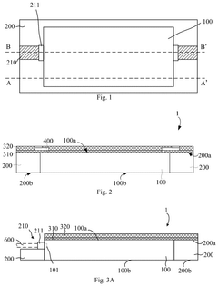
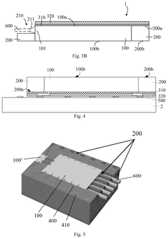
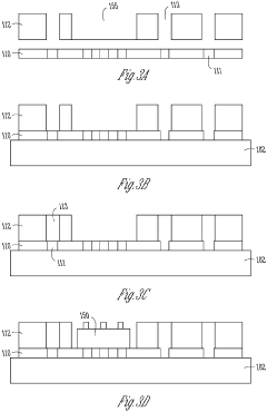
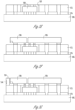
Silicon photonic chip package module based on plastic encapsulation
PatentPendingUS20250291137A1
Innovation
- The proposed silicon photonic chip package module includes a transparent cushioning material layer covering the port of the silicon photonic chip, a plastic encapsulation layer with grooves for fiber optics, and a metal interconnect layer replacing conventional metal wires, allowing direct optical connection to a fiber optic and reducing alignment errors.
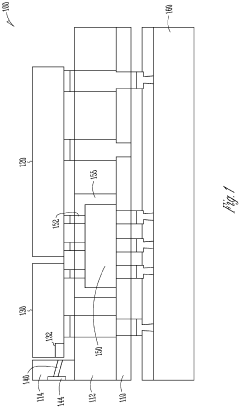
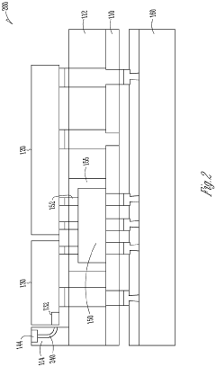
Semiconductor assembly with waveguide and glass substrate
PatentPendingEP4191307A1
Innovation
- The use of laser-based technology for integrating photonic integrated circuits, electronic integrated circuits, and substrates with low-loss coupling, including laser-made glass-to-glass bonds and embedded waveguides formed through laser direct writing, addresses these challenges by minimizing coupling loss and enabling high-voltage compatibility.
Regulatory Compliance Framework
The regulatory landscape for silicon photonics packaging spans multiple jurisdictions and technical domains, creating a complex compliance environment for manufacturers and developers. At the international level, organizations such as the International Electrotechnical Commission (IEC) and the International Organization for Standardization (ISO) have established foundational standards that address aspects of photonic integrated circuits, though many are still evolving to fully accommodate silicon photonics packaging specificities.
In the United States, the Federal Communications Commission (FCC) regulates electromagnetic compatibility aspects, while the Food and Drug Administration (FDA) oversees medical applications of silicon photonics. The European Union implements the RoHS (Restriction of Hazardous Substances) and REACH (Registration, Evaluation, Authorization and Restriction of Chemicals) directives, which significantly impact material selection for packaging solutions, particularly regarding lead-free solder requirements and chemical treatments.
Telecommunications standards bodies, including the IEEE and ITU, have developed specifications for optical transceivers that indirectly influence packaging requirements. These standards primarily focus on performance metrics rather than manufacturing processes, creating a gap in regulatory guidance specific to packaging technologies.
Environmental regulations present particular challenges for silicon photonics packaging. The hermetic sealing processes often involve materials and chemicals that face increasing restrictions under global environmental protocols. Temperature cycling requirements for reliability testing must align with standards such as Telcordia GR-468, while simultaneously meeting environmental compliance targets.
Certification pathways remain fragmented across different application domains. Data center applications follow one set of compliance requirements, while automotive LIDAR systems must adhere to more stringent safety and reliability standards such as ISO 26262. Medical diagnostic applications introduce yet another layer of regulatory scrutiny, with requirements for biocompatibility and sterilization resistance.
Industry consortia have begun developing self-regulatory frameworks to address these gaps. The Consortium for On-Board Optics (COBO) and the Optical Internetworking Forum (OIF) have published implementation agreements that serve as de facto standards for certain packaging approaches, providing interim guidance while formal regulatory frameworks mature.
Successful navigation of this complex regulatory landscape requires a comprehensive compliance strategy that anticipates regulatory evolution. Companies must implement robust documentation systems that track material compositions, manufacturing processes, and test results against multiple regulatory frameworks simultaneously. Cross-functional teams comprising regulatory experts, materials scientists, and packaging engineers are increasingly essential to address compliance challenges proactively rather than reactively.
Environmental Impact Assessment
The environmental impact of silicon photonics packaging represents a critical consideration in the technology's regulatory landscape. Manufacturing processes for silicon photonics components involve numerous materials with varying environmental footprints, including silicon, germanium, indium phosphide, and various metals for interconnects. These materials require energy-intensive fabrication methods and often utilize hazardous chemicals for etching and cleaning processes, raising significant environmental concerns.
Regulatory frameworks worldwide increasingly demand comprehensive life cycle assessments for photonic components. The European Union's Restriction of Hazardous Substances (RoHS) and Registration, Evaluation, Authorization and Restriction of Chemicals (REACH) regulations specifically impact material selection and manufacturing processes in silicon photonics packaging. Similarly, the United States Environmental Protection Agency enforces strict guidelines on chemical usage and disposal relevant to semiconductor manufacturing.
Energy consumption during silicon photonics manufacturing presents another environmental challenge. The high-precision equipment required for packaging operations, including laser welding systems and vacuum deposition chambers, consumes substantial electricity. Regulatory bodies are implementing progressively stringent energy efficiency standards that manufacturers must meet, potentially increasing production costs but reducing long-term environmental impact.
Waste management constitutes a significant regulatory hurdle in silicon photonics packaging. The industry generates various waste streams, including chemical byproducts, excess materials, and end-of-life components. Regulations governing electronic waste disposal vary globally, creating compliance challenges for companies operating across multiple jurisdictions. The Basel Convention on hazardous waste movement further complicates international supply chains for silicon photonics components.
Despite these challenges, silicon photonics offers substantial environmental benefits compared to traditional electronic systems. The technology enables significant energy savings in data centers through reduced power consumption and heat generation. These advantages have prompted regulatory incentives in some regions, including tax benefits and research grants for companies developing energy-efficient photonic solutions.
Industry leaders are implementing innovative approaches to address environmental regulatory challenges. These include developing lead-free soldering techniques, implementing closed-loop chemical recycling systems, and designing components for easier disassembly and material recovery. Such proactive measures not only ensure regulatory compliance but also position companies favorably as environmental regulations continue to evolve.
The path toward environmentally sustainable silicon photonics packaging requires collaborative efforts between industry stakeholders, regulatory bodies, and research institutions. Standardization of environmental impact assessment methodologies specific to photonic technologies would significantly benefit the industry by providing clear compliance guidelines and facilitating international market access.
Unlock deeper insights with PatSnap Eureka Quick Research — get a full tech report to explore trends and direct your research. Try now!
Generate Your Research Report Instantly with AI Agent
Supercharge your innovation with PatSnap Eureka AI Agent Platform!