Silicon Photonics Packaging: Regulatory and Market Analysis
SEP 29, 20259 MIN READ
Generate Your Research Report Instantly with AI Agent
Patsnap Eureka helps you evaluate technical feasibility & market potential.
Silicon Photonics Evolution and Objectives
Silicon photonics has evolved significantly since its conceptual inception in the late 1980s, transitioning from theoretical research to commercial applications over the past three decades. The field emerged from the convergence of semiconductor manufacturing techniques and optical communication principles, aiming to leverage silicon's properties for photonic applications despite its indirect bandgap limitations.
The 1990s marked the foundational research phase, with pioneering work at institutions like MIT and Stanford establishing the theoretical framework for silicon-based photonic devices. By the early 2000s, researchers demonstrated the first practical silicon modulators and waveguides, albeit with performance limitations compared to traditional photonic materials.
A significant acceleration occurred between 2005-2015, characterized by breakthroughs in hybrid integration techniques that combined silicon with III-V materials to overcome silicon's inherent limitations in light emission. This period saw the development of critical components including high-speed modulators, efficient photodetectors, and wavelength division multiplexing (WDM) systems on silicon platforms.
The packaging of silicon photonics has presented persistent challenges throughout this evolution. Traditional optical packaging techniques proved inadequate for the precision and scale required by silicon photonic integrated circuits (PICs). The industry has progressively moved from manual alignment methods toward automated, wafer-level packaging solutions to address cost and scalability concerns.
Current technological objectives focus on several key areas: reducing coupling losses between optical fibers and silicon waveguides, which remain a significant performance bottleneck; developing standardized packaging platforms that can accommodate diverse photonic components; and creating thermally stable packaging solutions that mitigate silicon's temperature sensitivity.
Long-term objectives include achieving fully automated, high-volume manufacturing capabilities for silicon photonic packages, comparable to electronic integrated circuit production. The industry aims to reduce packaging costs from the current 60-80% of total device cost to below 30%, making silicon photonics economically viable for mass-market applications beyond data centers.
Regulatory considerations have evolved alongside the technology, with standards bodies like IEC, IEEE, and Telcordia developing specifications for reliability, interoperability, and performance. These standards are increasingly important as silicon photonics moves from specialized applications toward consumer markets, where regulatory compliance becomes a prerequisite for market entry.
Market Demand for Integrated Photonic Solutions
The integrated photonics market is experiencing unprecedented growth, driven by increasing demands for high-speed data transmission, advanced sensing capabilities, and miniaturized optical components. Current market analyses indicate that the global silicon photonics market is projected to reach $3.5 billion by 2025, with a compound annual growth rate exceeding 20% between 2020-2025. This remarkable expansion reflects the critical role integrated photonic solutions play in addressing bandwidth limitations of traditional electronic systems.
Data centers represent the largest market segment for integrated photonics, accounting for approximately 35% of total demand. The exponential increase in cloud computing, video streaming, and IoT applications has created an urgent need for higher bandwidth and energy-efficient interconnects. Major data center operators including Google, Amazon, and Microsoft are actively implementing silicon photonics solutions to overcome the bottlenecks in their infrastructure, particularly for distances exceeding 500 meters where traditional copper interconnects become inefficient.
Telecommunications constitutes the second-largest market segment, with carriers seeking cost-effective solutions for 5G infrastructure deployment and fiber-to-the-home networks. The demand for coherent optical transceivers utilizing silicon photonics has grown substantially, offering significant advantages in size, power consumption, and cost compared to discrete optical components. Industry reports indicate that integrated photonic solutions can reduce power consumption by up to 30% while increasing data transmission rates to 400Gbps and beyond.
Emerging applications in automotive LiDAR, biosensing, and quantum computing are creating new market opportunities for integrated photonics. The automotive sector alone is expected to generate demand worth $500 million by 2025 as autonomous driving technologies mature. Medical diagnostics represents another high-growth segment, with integrated photonic biosensors enabling rapid, point-of-care testing capabilities that were previously confined to specialized laboratories.
Regional analysis reveals that North America currently leads the market with approximately 40% share, followed by Asia-Pacific at 35% and Europe at 20%. However, the Asia-Pacific region is demonstrating the fastest growth rate, driven by substantial investments in telecommunications infrastructure and manufacturing capabilities in China, Taiwan, and Singapore. Government initiatives supporting photonics research and development, such as China's "Made in China 2025" and the European Photonics21 program, are further accelerating market expansion in these regions.
Customer requirements are increasingly focused on standardized packaging solutions that can reduce integration costs, which currently represent up to 80% of the total module cost. End-users across industries are demanding plug-and-play photonic components with simplified interfaces that can be readily incorporated into existing systems without specialized optical expertise.
Current Packaging Challenges and Limitations
Silicon photonics packaging faces significant technical challenges that currently limit widespread commercial adoption. The primary obstacle remains the precise alignment requirements between optical components. Sub-micron alignment precision is necessary for efficient coupling between photonic integrated circuits (PICs) and optical fibers, with tolerances often below 0.1μm. This level of precision demands specialized equipment and processes that substantially increase manufacturing costs and complexity.
Thermal management presents another critical challenge. Silicon photonics devices are highly temperature-sensitive, with wavelength shifts of approximately 0.1nm/°C. Without proper thermal control, performance degradation occurs across operating conditions, making reliable deployment difficult in variable environments. Current packaging solutions struggle to provide adequate thermal stability while maintaining compact form factors.
Hermeticity requirements further complicate packaging designs. Optical components are vulnerable to environmental contaminants, particularly moisture, which can cause performance degradation over time. Traditional hermetic sealing techniques using metal packages are often incompatible with the need for optical fiber access points, creating design conflicts between environmental protection and functionality.
Cost-effective scaling remains elusive in current packaging approaches. While silicon photonics fabrication has benefited from CMOS manufacturing techniques, packaging processes have not achieved similar economies of scale. Manual alignment and assembly steps persist in many production lines, creating bottlenecks that prevent true high-volume manufacturing. The cost of packaging frequently exceeds 60-80% of the total device cost, undermining the economic advantages of silicon photonics technology.
Standardization gaps present significant market barriers. Unlike electronic components with well-established packaging standards, silicon photonics lacks industry-wide standardization for interfaces, testing protocols, and form factors. This fragmentation forces companies to develop proprietary solutions, hindering interoperability and increasing development costs across the ecosystem.
Material compatibility issues between silicon photonics and conventional packaging materials create reliability concerns. Coefficient of thermal expansion (CTE) mismatches between silicon and packaging materials can induce stress during temperature cycling, potentially causing optical misalignment or component failure. Current solutions often involve complex material systems that add cost and manufacturing complexity.
Testing methodologies for packaged devices remain inadequate for high-volume production. Unlike electronic components with standardized testing approaches, optical testing of packaged photonic devices requires specialized equipment and procedures. The lack of efficient, automated testing solutions creates quality assurance challenges and increases production costs.
Packaging Solutions and Methodologies
01 Optical coupling techniques in silicon photonics packaging
Various optical coupling techniques are employed in silicon photonics packaging to efficiently transfer light between optical components. These include edge coupling, grating couplers, and evanescent coupling methods that minimize insertion loss. Advanced alignment techniques ensure precise positioning of optical fibers relative to photonic waveguides, which is critical for maintaining signal integrity in high-speed data transmission applications.- Optical coupling techniques in silicon photonics packaging: Various optical coupling techniques are employed in silicon photonics packaging to efficiently transfer light between optical components. These include edge coupling, grating couplers, and evanescent coupling methods that minimize insertion loss. Advanced alignment techniques ensure precise positioning of optical components to maintain signal integrity across interfaces. These coupling solutions address the critical challenge of connecting silicon photonic chips to optical fibers and other photonic components.
- Thermal management solutions for silicon photonics: Thermal management is crucial in silicon photonics packaging to maintain stable operation of temperature-sensitive components. Solutions include integrated thermoelectric coolers, heat spreaders, and thermally conductive materials that efficiently dissipate heat. Advanced thermal designs incorporate heat sinks and thermal vias to manage temperature gradients across the package. These approaches help maintain wavelength stability and prevent performance degradation in silicon photonic devices operating at high data rates.
- Integration of electronic and photonic components: Hybrid integration of electronic and photonic components enables high-performance silicon photonic systems. Techniques include 2.5D and 3D integration approaches, flip-chip bonding, and through-silicon vias (TSVs) that create compact, multi-functional packages. Co-packaging of drivers, transimpedance amplifiers, and control electronics with photonic integrated circuits reduces parasitic effects and improves signal integrity. These integration methods support high-bandwidth data transmission while minimizing power consumption and footprint.
- Hermetic sealing and environmental protection: Hermetic sealing and environmental protection techniques safeguard silicon photonic devices from moisture, contaminants, and mechanical stress. Methods include glass lid bonding, metal sealing rings, and specialized polymer encapsulation that maintain optical transparency while providing robust protection. Advanced packaging materials with controlled coefficient of thermal expansion (CTE) prevent stress-induced birefringence and wavelength shifts. These protection strategies ensure long-term reliability and stable performance in varying environmental conditions.
- Wafer-level packaging processes for silicon photonics: Wafer-level packaging processes enable cost-effective, high-volume manufacturing of silicon photonic devices. Techniques include wafer bonding, collective alignment, and simultaneous testing of multiple dies that improve throughput and yield. Advanced lithography and etching processes create precise optical features and alignment structures directly on the wafer. These manufacturing approaches reduce assembly costs while maintaining high performance and reliability, supporting the commercial viability of silicon photonic technologies.
02 Thermal management solutions for silicon photonics
Thermal management is crucial in silicon photonics packaging due to the temperature sensitivity of optical components. Solutions include integration of thermal interface materials, heat spreaders, and active cooling systems to maintain stable operating temperatures. These approaches help mitigate wavelength drift, reduce signal degradation, and ensure reliable performance of photonic integrated circuits in various environmental conditions.Expand Specific Solutions03 Integration of electronic and photonic components
Hybrid integration approaches combine electronic and photonic components in a single package to enable high-performance optoelectronic systems. Techniques include flip-chip bonding, through-silicon vias, and interposer technologies that facilitate electrical and optical interconnections. These integration methods address challenges related to signal integrity, power delivery, and form factor constraints in next-generation communication systems.Expand Specific Solutions04 Hermetic sealing and environmental protection
Hermetic sealing techniques protect sensitive silicon photonic components from environmental factors such as moisture, dust, and chemical contaminants. Methods include glass lid bonding, metal sealing, and polymer encapsulation that maintain package integrity while allowing optical transmission. These protection strategies are essential for ensuring long-term reliability and performance stability of photonic integrated circuits in harsh operating environments.Expand Specific Solutions05 Wafer-level packaging for silicon photonics
Wafer-level packaging technologies enable cost-effective mass production of silicon photonic devices. These approaches include wafer bonding, through-silicon via formation, and collective assembly processes that facilitate parallel processing of multiple devices. By integrating optical, electrical, and mechanical functions at the wafer level, manufacturers can achieve higher throughput, improved yield, and reduced form factors for silicon photonic systems.Expand Specific Solutions
Key Industry Players and Ecosystem
Silicon photonics packaging is currently in a growth phase, with the market expected to expand significantly due to increasing demand for high-speed data transmission and energy-efficient computing solutions. The global market size is projected to reach several billion dollars by 2030, driven by applications in data centers, telecommunications, and emerging AI infrastructure. Technologically, the field is advancing rapidly but remains challenging, with companies at varying maturity levels. Industry leaders like Intel, TSMC, and GlobalFoundries have established commercial production capabilities, while Huawei, IBM, and Lumentum are making significant R&D investments. Specialized players such as Aeponyx and Vanguard Automation are developing innovative packaging solutions. The ecosystem is further strengthened by collaborations between semiconductor manufacturers, equipment providers, and research institutions, creating a competitive landscape that balances established players with emerging specialists.
Taiwan Semiconductor Manufacturing Co., Ltd.
Technical Solution: TSMC has developed advanced silicon photonics packaging technologies focusing on heterogeneous integration of photonic and electronic components. Their approach utilizes their advanced semiconductor manufacturing capabilities, including their 3D IC and advanced packaging technologies like Chip-on-Wafer-on-Substrate (CoWoS) and Integrated Fan-Out (InFO) platforms adapted for photonic applications. TSMC's silicon photonics packaging solution incorporates precision optical alignment techniques with tolerances below 0.5μm to ensure optimal coupling efficiency between optical fibers and on-chip waveguides. They've pioneered hermetic sealing techniques specifically designed to protect sensitive photonic components while maintaining optical transparency where needed. TSMC's manufacturing process includes specialized handling procedures to prevent contamination of optical surfaces and employs automated testing systems for both electronic and optical performance verification. Their packaging solutions support data rates exceeding 400Gbps per channel with a roadmap to reach terabit speeds.
Strengths: World-class semiconductor manufacturing infrastructure; extensive experience in advanced packaging technologies; ability to leverage existing manufacturing processes for economies of scale. Weaknesses: Relatively newer entrant to silicon photonics compared to some competitors; challenges in optical alignment precision at high volumes; higher initial capital investment requirements for specialized equipment.
Intel Corp.
Technical Solution: Intel has pioneered advanced silicon photonics packaging solutions through their integrated approach combining photonic and electronic components on a single chip. Their technology utilizes a hybrid integration method where silicon photonic chips are coupled with electronic ICs using advanced flip-chip bonding techniques. Intel's Co-Packaged Optics (CPO) platform integrates optical transceivers directly with switch ASICs, significantly reducing power consumption and increasing bandwidth density. Their manufacturing process employs 300mm wafer technology with automated assembly lines for high-volume production. Intel has developed proprietary optical coupling techniques that achieve less than 1dB insertion loss between fiber and silicon waveguides. Their packaging solutions address thermal management challenges through specialized heat dissipation structures and materials that maintain optical alignment despite temperature fluctuations.
Strengths: Industry-leading manufacturing infrastructure allowing for high-volume production; vertical integration capabilities from design to fabrication; extensive IP portfolio in silicon photonics. Weaknesses: Higher production costs compared to traditional electronic packaging; thermal management challenges in dense photonic-electronic integration; relatively complex assembly process requiring precise alignment.
Critical Patents and Technical Innovations
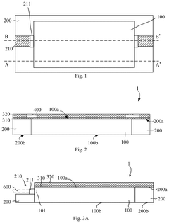
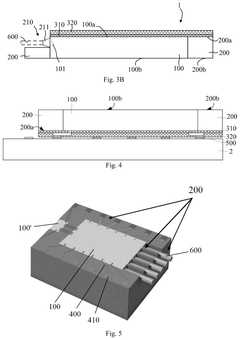
Silicon photonic chip package module based on plastic encapsulation
PatentPendingUS20250291137A1
Innovation
- The proposed silicon photonic chip package module includes a transparent cushioning material layer covering the port of the silicon photonic chip, a plastic encapsulation layer with grooves for fiber optics, and a metal interconnect layer replacing conventional metal wires, allowing direct optical connection to a fiber optic and reducing alignment errors.
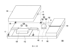
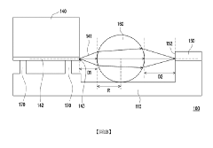
Silicon photonic package structure
PatentActiveTW202120978A
Innovation
- A silicon photonic packaging structure incorporating a substrate with a conductive bump, barrier structure, laser diode, mode converter, and spherical lens, where the spherical lens converges light to the mode converter and the barrier structure prevents conductive bump overflow, reducing precision needs and maintaining light efficiency.
Regulatory Framework and Compliance
Silicon photonics packaging operates within a complex regulatory landscape that varies significantly across global markets. In the United States, the FDA maintains oversight of photonic devices used in medical applications, while the FCC regulates telecommunications applications through standards for electromagnetic compatibility and signal integrity. The European Union implements more stringent requirements through the RoHS (Restriction of Hazardous Substances) and REACH (Registration, Evaluation, Authorization and Restriction of Chemicals) directives, which restrict the use of certain hazardous materials in electronic and photonic components.
The International Electrotechnical Commission (IEC) has established several standards specifically addressing silicon photonics, including IEC 62149 for fiber optic active components and IEC 60825 for laser safety classifications. These standards provide crucial frameworks for manufacturers to ensure compliance across international markets. Additionally, the Telcordia GR-468-CORE reliability standard has become a de facto requirement for photonic components in telecommunications infrastructure.
Environmental regulations present significant challenges for silicon photonics packaging. The industry must navigate end-of-life product management regulations such as the EU's Waste Electrical and Electronic Equipment (WEEE) directive, which mandates specific recycling procedures for photonic components. Temperature cycling requirements and hermetic sealing specifications further complicate compliance efforts, particularly for applications in harsh environments.
Certification processes for silicon photonics packages vary by application domain and geographic region. Medical applications require extensive clinical validation and safety certification, while automotive applications must meet stringent reliability standards such as AEC-Q100 for integrated circuits. The telecommunications sector typically requires compliance with network equipment standards from organizations like ETSI in Europe or Telcordia in North America.
Recent regulatory trends indicate increasing scrutiny of rare earth elements and specialized materials used in photonics manufacturing. China's export restrictions on certain rare earth materials have prompted regulatory bodies in the US and EU to develop strategic frameworks for securing supply chains. Additionally, emerging regulations around quantum-secure communications are beginning to impact silicon photonics packaging requirements, particularly for government and financial sector applications.
Compliance costs represent a significant portion of overall development expenses for silicon photonics products. Industry analysis suggests that regulatory testing and certification typically accounts for 15-20% of total product development costs, with this percentage rising for applications in highly regulated sectors such as healthcare, aerospace, and defense. Companies must carefully balance these compliance investments against time-to-market pressures in the rapidly evolving photonics landscape.
Supply Chain Resilience
The silicon photonics packaging supply chain faces unique vulnerabilities that require strategic management approaches. The global nature of semiconductor manufacturing creates inherent dependencies across multiple regions, with critical components often sourced from limited suppliers. For silicon photonics specifically, the supply chain complexity is magnified by the integration of optical and electronic components, requiring specialized materials and manufacturing processes that are concentrated in select geographic locations.
Recent global disruptions, including the COVID-19 pandemic, geopolitical tensions, and natural disasters, have exposed significant weaknesses in the silicon photonics supply chain. Manufacturing bottlenecks in key regions like Taiwan and Japan have led to extended lead times and production delays, while trade restrictions between major economies have complicated access to essential components and technologies. These vulnerabilities have prompted industry stakeholders to reevaluate their supply chain strategies.
Regulatory frameworks across different jurisdictions further complicate supply chain resilience efforts. Export controls on advanced technologies, particularly those with potential dual-use applications, create compliance challenges for global silicon photonics manufacturers. Different environmental and safety standards between regions necessitate adaptive manufacturing approaches, while intellectual property protection varies significantly across key markets, affecting technology transfer and collaboration.
Building resilience in the silicon photonics packaging supply chain requires multi-faceted approaches. Diversification of supplier networks across different geographic regions can mitigate regional disruption risks, while strategic inventory management with appropriate buffer stocks helps absorb short-term supply shocks. Vertical integration strategies, where companies control multiple stages of the production process, are increasingly being adopted to reduce external dependencies.
Advanced technologies are playing a crucial role in enhancing supply chain visibility and resilience. Digital twin technologies enable real-time monitoring and simulation of supply chain operations, while blockchain solutions improve traceability and authentication of components. AI-powered predictive analytics help anticipate potential disruptions and optimize inventory levels accordingly.
Industry collaboration initiatives are emerging as essential components of resilience strategies. Consortium approaches for shared manufacturing capabilities reduce individual company vulnerabilities, while standardization efforts simplify component interchangeability and reduce dependency on specific suppliers. Public-private partnerships are also developing to address critical infrastructure needs and ensure long-term supply chain stability in this strategically important technology sector.
Unlock deeper insights with Patsnap Eureka Quick Research — get a full tech report to explore trends and direct your research. Try now!
Generate Your Research Report Instantly with AI Agent
Supercharge your innovation with Patsnap Eureka AI Agent Platform!