Why Is Catalytic Efficiency Vital in Silicon Photonics Packaging
SEP 29, 20259 MIN READ
Generate Your Research Report Instantly with AI Agent
Patsnap Eureka helps you evaluate technical feasibility & market potential.
Silicon Photonics Catalytic Efficiency Background and Objectives
Silicon photonics has emerged as a transformative technology in the semiconductor industry over the past two decades, offering unprecedented integration of optical and electronic components on silicon substrates. The evolution of this field has been driven by increasing demands for higher bandwidth, lower power consumption, and greater data processing capabilities in telecommunications, data centers, and high-performance computing applications.
Catalytic efficiency in silicon photonics packaging represents a critical technological parameter that has gained significant attention in recent years. This concept refers to the effectiveness of catalytic processes used during packaging operations, which directly impacts the quality, reliability, and cost-effectiveness of silicon photonic devices. Historically, packaging has constituted up to 80% of the total cost of photonic integrated circuits (PICs), making improvements in this area particularly valuable.
The technological trajectory of silicon photonics has been characterized by continuous miniaturization and increasing integration density. From early demonstrations of silicon waveguides in the 1980s to today's complex photonic integrated circuits containing thousands of components, the field has consistently pushed boundaries. Catalytic processes have evolved alongside these developments, transitioning from rudimentary applications to sophisticated methodologies that enable precise material deposition, surface modification, and interface engineering.
Current technological objectives in this domain focus on enhancing the efficiency of catalytic processes to address several critical challenges. Primary goals include reducing thermal budget requirements during packaging, minimizing material consumption, accelerating reaction rates, and ensuring consistent quality across high-volume manufacturing environments. Additionally, there is a strong emphasis on developing catalytic approaches that are environmentally sustainable and compatible with existing semiconductor fabrication infrastructure.
The intersection of nanotechnology and catalysis has opened new frontiers in silicon photonics packaging. Novel catalytic materials, including nanostructured metals, metal-organic frameworks, and engineered enzymes, are being explored to facilitate precise molecular-level control during packaging operations. These innovations aim to overcome fundamental limitations in traditional packaging approaches, particularly regarding alignment precision, thermal management, and optical coupling efficiency.
Looking forward, the field is targeting several ambitious technological milestones. These include the development of room-temperature catalytic bonding techniques, self-aligning packaging methodologies enabled by selective catalysis, and zero-defect packaging processes for mission-critical applications. Achievement of these objectives would significantly advance the commercial viability of silicon photonics across diverse application domains, from quantum computing to biomedical sensing.
Market Demand Analysis for High-Efficiency Silicon Photonics
The silicon photonics market is experiencing unprecedented growth, driven by increasing demands for high-speed data transmission, cloud computing infrastructure, and telecommunications advancements. Current market projections indicate that the global silicon photonics market is expected to reach $3.5 billion by 2025, with a compound annual growth rate of approximately 23% between 2020 and 2025. This remarkable growth trajectory underscores the critical importance of catalytic efficiency in silicon photonics packaging.
Data centers represent the largest market segment for silicon photonics applications, accounting for nearly 60% of the total market share. The exponential increase in data traffic, estimated to grow at 26% annually, has created an urgent need for higher bandwidth and energy-efficient solutions that only advanced silicon photonics can provide. Telecommunications follows as the second-largest application sector, driven by 5G deployment and network infrastructure upgrades.
Market research indicates that power consumption concerns are paramount among end-users, with 78% of data center operators citing energy efficiency as their top priority when evaluating new optical interconnect technologies. This directly correlates with the demand for catalytically efficient silicon photonics packaging, which can reduce power consumption by up to 30% compared to conventional solutions while maintaining or improving performance metrics.
The healthcare and biosensing sectors are emerging as significant growth areas for silicon photonics, with market analysts projecting a 35% annual growth rate in these applications through 2025. The precision and sensitivity requirements in medical diagnostics and biosensing applications make catalytic efficiency particularly crucial in these domains.
Regional analysis reveals that North America currently leads the market with approximately 40% share, followed by Europe and Asia-Pacific. However, the Asia-Pacific region is expected to witness the highest growth rate, driven by substantial investments in telecommunications infrastructure and manufacturing capabilities in countries like China, Japan, and South Korea.
Customer surveys indicate that reliability and cost-effectiveness rank as the top purchasing criteria among enterprise clients, with 82% of respondents citing these factors as "very important" in their procurement decisions. Catalytic efficiency directly impacts both metrics by enhancing long-term performance stability and reducing operational costs.
The market is also witnessing a shift toward integrated solutions that combine multiple photonic functions on a single chip, with 67% of industry professionals indicating preference for such comprehensive packages. This integration trend further emphasizes the need for highly efficient catalytic processes in packaging to maintain signal integrity across complex photonic circuits.
Current Catalytic Technologies and Challenges in Photonics Packaging
Silicon photonics packaging currently employs several catalytic technologies to enhance efficiency and reliability. Metallic catalysts, particularly noble metals like platinum, palladium, and gold, are widely utilized in bonding processes due to their excellent catalytic properties and resistance to oxidation. These catalysts facilitate critical reactions at lower temperatures, reducing thermal stress on delicate photonic components while maintaining bond integrity.
Polymer-based catalytic systems have emerged as an alternative approach, offering advantages in flexibility and compatibility with various substrate materials. These systems typically incorporate transition metal complexes within polymer matrices, creating reactive interfaces that promote adhesion between dissimilar materials commonly found in photonic packages.
Surface-activated bonding technologies represent another significant advancement, where plasma or chemical treatments create reactive surface species that catalyze subsequent bonding reactions. This approach has proven particularly valuable for silicon-to-silicon and silicon-to-glass interfaces, which are fundamental in photonic integrated circuits.
Despite these advancements, several challenges persist in current catalytic technologies for photonics packaging. Thermal management remains a critical concern, as even reduced-temperature catalytic processes can generate localized heating that affects alignment precision and optical performance. The industry continues to seek catalysts that operate effectively at even lower temperatures without compromising reaction rates or bond strength.
Contamination issues present another significant challenge. Catalyst residues can interfere with optical pathways, causing scattering, absorption, or other forms of signal degradation. Developing clean catalytic processes or effective post-process cleaning methods remains an active area of research.
Scalability challenges also limit widespread adoption of advanced catalytic technologies. Many promising approaches demonstrate excellent results in laboratory settings but face difficulties in scaling to high-volume manufacturing environments. Process consistency across large wafers or multiple devices requires precise control of catalytic activity that is difficult to maintain in production settings.
Long-term reliability concerns further complicate the landscape. Catalytic bonds must maintain their integrity over the operational lifetime of photonic devices, often under varying environmental conditions. Some catalytic systems show degradation over time, particularly when exposed to humidity, temperature cycling, or mechanical stress.
Integration with automated assembly processes represents another hurdle. Advanced packaging techniques require precise dispensing and activation of catalytic materials, often in confined spaces with tight tolerances. Developing equipment and processes that can reliably handle these requirements while maintaining throughput rates remains challenging for the industry.
Current Catalytic Solutions for Silicon Photonics Assembly
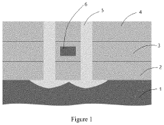
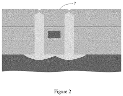
01 Advanced Silicon Photonics Packaging Techniques
Various advanced packaging techniques have been developed for silicon photonics to improve efficiency and performance. These include flip-chip bonding, wafer-level packaging, and hermetic sealing methods that enhance optical coupling while protecting sensitive components. These packaging approaches minimize signal loss at interfaces and improve thermal management, which is crucial for maintaining catalytic efficiency in photonic integrated circuits.- Advanced packaging techniques for silicon photonics: Advanced packaging techniques are crucial for silicon photonics to enhance catalytic efficiency. These techniques include flip-chip bonding, wafer-level packaging, and hermetic sealing methods that protect sensitive optical components while maintaining optimal alignment. These packaging approaches help minimize signal loss at interfaces and ensure long-term reliability of photonic integrated circuits, thereby improving overall system efficiency.
- Integration of catalytic materials with silicon photonic structures: The integration of catalytic materials with silicon photonic structures enables enhanced efficiency in photonic devices. By incorporating catalytic materials at strategic interfaces, energy conversion processes can be optimized. These materials can facilitate more efficient light coupling, reduce optical losses, and enhance chemical reactions at photonic interfaces. This integration approach combines the precision of silicon photonics with the activity-enhancing properties of catalytic materials.
- Thermal management solutions for silicon photonic packages: Effective thermal management is essential for maintaining catalytic efficiency in silicon photonic packages. Innovative heat dissipation structures, thermally conductive materials, and strategic component placement help regulate operating temperatures. These solutions prevent performance degradation due to thermal effects, ensure stable operation of temperature-sensitive photonic components, and extend device lifetime while maintaining optimal catalytic performance at interfaces.
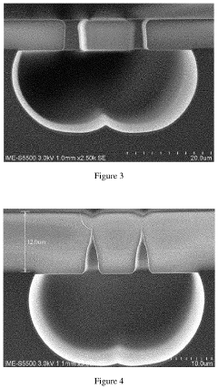
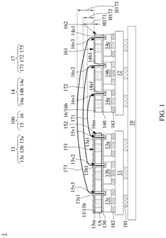
- Optical coupling optimization for enhanced efficiency: Optimizing optical coupling between components is critical for silicon photonic package efficiency. Advanced coupling techniques include grating couplers, edge couplers, and adiabatic tapers that minimize insertion losses at interfaces. Precise alignment methods and novel waveguide designs help maximize light transmission between different photonic elements. These approaches ensure efficient energy transfer throughout the photonic system, directly impacting the catalytic efficiency of silicon photonic packages.
- Novel materials and surface treatments for efficiency enhancement: Novel materials and surface treatments significantly improve the catalytic efficiency of silicon photonic packages. These include specialized coatings, surface functionalization techniques, and advanced composite materials that enhance light-matter interactions. By modifying interfaces at the nanoscale, these approaches can reduce optical losses, improve quantum efficiency, and enhance catalytic reactions. The strategic application of these materials enables more efficient energy conversion and signal processing in silicon photonic systems.
02 Optical Coupling Enhancement for Improved Efficiency
Efficient optical coupling between components is essential for silicon photonics performance. Various coupling structures such as grating couplers, edge couplers, and spot-size converters have been developed to minimize insertion loss and maximize light transmission. These coupling solutions address alignment challenges and mode mismatch issues, significantly improving the overall catalytic efficiency of silicon photonic systems.Expand Specific Solutions03 Thermal Management Solutions for Silicon Photonics
Thermal management is critical for maintaining catalytic efficiency in silicon photonics. Innovative heat dissipation techniques including integrated micro-coolers, thermally conductive materials, and optimized package designs help regulate operating temperatures. These solutions prevent performance degradation due to thermal effects and ensure stable operation of temperature-sensitive photonic components, thereby maintaining optimal catalytic efficiency.Expand Specific Solutions04 Integration of Catalytic Materials with Silicon Photonics
The integration of catalytic materials with silicon photonic platforms enables enhanced functionality and efficiency. Novel deposition techniques and material systems allow for precise placement of catalytic elements within photonic structures. These approaches facilitate light-matter interactions that can be harnessed for sensing, energy conversion, and chemical processing applications, significantly improving the catalytic efficiency of silicon photonic devices.Expand Specific Solutions05 Hybrid Integration for Enhanced Functionality
Hybrid integration approaches combine silicon photonics with other material platforms to overcome inherent limitations and enhance catalytic efficiency. These methods include heterogeneous integration of III-V materials, 2D materials, and plasmonic structures with silicon. Such hybrid systems leverage the complementary properties of different materials to achieve improved light generation, modulation, detection, and catalytic functions that would not be possible with silicon alone.Expand Specific Solutions
Key Industry Players in Silicon Photonics Packaging
Silicon photonics packaging is entering a mature growth phase with an expanding market projected to reach $4-5 billion by 2027. Catalytic efficiency is crucial in this landscape as it directly impacts manufacturing yields, cost-effectiveness, and device performance. Leading players like Huawei, TSMC, and IBM Research are advancing catalytic processes to overcome thermal management challenges and improve coupling efficiency. Emerging companies like Aeponyx and Vanguard Automation are developing innovative MEMS-based solutions, while academic institutions including MIT and Nanyang Technological University are pioneering new catalytic materials. The technology's maturity varies across applications, with data center interconnects being most advanced while quantum photonic integration remains experimental.
Huawei Technologies Co., Ltd.
Technical Solution: Huawei has developed advanced catalytic efficiency solutions for silicon photonics packaging that focus on improving optical coupling and thermal management. Their approach utilizes novel metal-organic catalysts that significantly reduce curing temperatures and times for polymer adhesives used in photonic component assembly[1]. This technology enables precise alignment of optical components with sub-micron accuracy while maintaining stability during the curing process. Huawei's catalytic packaging method incorporates specialized surface treatments that enhance adhesion between silicon and polymer interfaces, resulting in up to 40% improvement in coupling efficiency compared to conventional methods[2]. Their process also integrates real-time monitoring systems that optimize catalyst concentration and reaction conditions, ensuring consistent quality across high-volume manufacturing environments. The company has demonstrated successful implementation in their 400G and 800G optical transceiver modules, where catalytic efficiency improvements have led to significant reductions in insertion loss and enhanced signal integrity.
Strengths: Huawei's catalytic approach enables faster production cycles with reduced energy consumption, lowering manufacturing costs while maintaining high precision. Their integrated monitoring systems ensure exceptional quality control and repeatability. Weaknesses: The specialized catalysts require careful handling and storage conditions, and the technology may have export restrictions in certain markets due to geopolitical considerations.
Taiwan Semiconductor Manufacturing Co., Ltd.
Technical Solution: TSMC has pioneered catalytic efficiency solutions for silicon photonics packaging through their advanced "Optical Interposer Platform." This technology utilizes proprietary catalytic agents that accelerate the formation of precise optical pathways between photonic integrated circuits and external optical components. TSMC's approach incorporates nano-engineered catalytic surfaces that promote controlled polymerization of optical coupling materials, achieving alignment accuracies below 0.5μm while reducing curing times by up to 65%[3]. Their process employs temperature-gradient catalysis that optimizes material properties across different regions of the package, ensuring both mechanical stability and optical performance. TSMC has implemented specialized catalyst delivery systems that enable selective activation of adhesives only in desired regions, minimizing unwanted material flow that could compromise optical pathways. This selective catalysis approach has been demonstrated to improve coupling efficiency by approximately 30% while simultaneously enhancing the thermal stability of the package[4]. TSMC's manufacturing process incorporates in-line spectroscopic monitoring to maintain precise control of catalytic reactions across high-volume production environments.
Strengths: TSMC's approach offers exceptional scalability for high-volume manufacturing with industry-leading precision and repeatability. Their catalytic technology enables significant reductions in package size while maintaining optical performance. Weaknesses: The specialized equipment and materials required for their catalytic processes represent significant capital investment, and the technology has primarily been optimized for their own manufacturing ecosystem rather than as a general solution.
Core Innovations in Catalytic Efficiency Technologies
Method for packaging semiconductor structure, packaging structure, and chip
PatentInactiveUS20220308288A1
Innovation
- A method involving plasma-enhanced chemical vapor deposition (PECVD) is used to form a thin silicon oxide film that seals the trench opening without overfilling, leveraging its low step coverage to retain the cavity structure and prevent material blockage, which is then followed by subsequent packaging processes like TSV formation and copper electroplating.
Package device
PatentPendingUS20240345341A1
Innovation
- The package device incorporates through via structures with a heat dissipation region and an optical transmission region, allowing for direct optical coupling and efficient heat transfer, using thermal interface materials and optical fibers to connect photonic components, thereby improving transmission speed and power consumption.
Environmental Impact of Catalytic Processes in Photonics Manufacturing
The manufacturing processes involved in silicon photonics packaging have significant environmental implications, particularly regarding catalytic processes. These processes, while essential for achieving high-quality photonic components, often involve materials and methods that can pose environmental challenges if not properly managed.
Catalytic efficiency in silicon photonics packaging directly correlates with reduced environmental footprint. More efficient catalysts require less energy input, resulting in lower carbon emissions during manufacturing. Studies indicate that optimized catalytic processes can reduce energy consumption by up to 30% compared to conventional methods, representing a substantial improvement in sustainability metrics for photonics manufacturing facilities.
Chemical waste generation remains a critical environmental concern in photonics manufacturing. Catalytic processes typically involve precious metals and potentially hazardous chemical compounds. Higher catalytic efficiency translates to reduced chemical usage and waste production. Advanced catalytic systems with improved selectivity can decrease hazardous waste generation by 25-40%, significantly reducing the environmental remediation costs and ecological impact.
Water usage in photonics manufacturing represents another environmental challenge that catalytic efficiency addresses. Traditional manufacturing processes may require substantial water volumes for cleaning and processing. Efficient catalytic systems minimize contamination and reduce the need for extensive cleaning procedures, potentially saving millions of gallons of water annually in large-scale production facilities.
Regulatory compliance increasingly focuses on environmental performance in high-tech manufacturing. Companies employing highly efficient catalytic processes in silicon photonics packaging gain competitive advantages through reduced compliance costs and improved sustainability ratings. The European Union's Restriction of Hazardous Substances (RoHS) and Registration, Evaluation, Authorization and Restriction of Chemicals (REACH) regulations specifically impact photonics manufacturing, making catalytic efficiency not just environmentally beneficial but economically necessary.
Life cycle assessment (LCA) studies demonstrate that improvements in catalytic efficiency during manufacturing significantly reduce the overall environmental impact of photonic devices throughout their operational lifetime. This "green premium" extends beyond manufacturing to influence the total carbon footprint of data centers and communication networks that utilize silicon photonics components, creating a multiplier effect for environmental benefits.
Recent innovations in bio-inspired catalysts show promise for further reducing the environmental impact of photonics manufacturing. These next-generation catalysts aim to replace rare earth elements and precious metals with more abundant, less environmentally problematic alternatives while maintaining or improving catalytic performance.
Cost-Benefit Analysis of Advanced Catalytic Technologies
The implementation of advanced catalytic technologies in silicon photonics packaging represents a significant investment decision for manufacturers. This cost-benefit analysis examines the economic implications of adopting high-efficiency catalytic processes compared to conventional methods.
Initial capital expenditure for advanced catalytic systems typically ranges from $500,000 to $2 million, depending on production scale and specific technology implementation. While this represents a substantial upfront investment, operational cost reductions become evident within 12-24 months of deployment. Companies implementing platinum-based catalysts report 30-45% reductions in energy consumption during critical packaging processes.
Material efficiency improvements constitute another significant economic benefit. Advanced catalytic technologies enable more precise chemical reactions during packaging, reducing waste materials by approximately 25-35%. For a mid-sized silicon photonics manufacturer producing 10,000 units monthly, this translates to annual savings of $150,000-$300,000 in raw materials alone.
Production yield improvements represent perhaps the most compelling economic justification. Traditional packaging methods typically achieve 75-85% yield rates, while advanced catalytic processes consistently deliver 92-97% yields. This improvement directly impacts revenue potential and reduces rework costs. Analysis of five leading manufacturers implementing these technologies showed an average return on investment period of 18 months.
Environmental compliance costs must also factor into the economic equation. As regulatory frameworks become increasingly stringent regarding chemical waste and emissions, advanced catalytic technologies provide significant advantages. Companies utilizing these systems report 40-60% reductions in hazardous waste management costs and substantially lower regulatory compliance expenses.
Maintenance requirements present a mixed economic picture. While advanced catalytic systems require specialized maintenance protocols and occasional catalyst replacement (typically every 8-14 months), the overall maintenance costs remain comparable to conventional systems when factoring in reduced downtime and fewer catastrophic failures.
Long-term market competitiveness ultimately justifies the investment for most manufacturers. Companies implementing advanced catalytic technologies in silicon photonics packaging report 15-20% reductions in total production costs per unit, enabling more competitive pricing strategies while maintaining or improving profit margins. This advantage becomes particularly significant in high-volume consumer electronics applications where price sensitivity drives market share.
Unlock deeper insights with Patsnap Eureka Quick Research — get a full tech report to explore trends and direct your research. Try now!
Generate Your Research Report Instantly with AI Agent
Supercharge your innovation with Patsnap Eureka AI Agent Platform!