

Silicon Photonics Packaging Materials for Electronics: An Overview
SEP 29, 202510 MIN READ
Generate Your Research Report Instantly with AI Agent
PatSnap Eureka helps you evaluate technical feasibility & market potential.
Silicon Photonics Evolution and Objectives
Silicon photonics has evolved significantly since its inception in the late 1980s, when researchers first began exploring the integration of optical components with silicon-based electronic circuits. The initial development phase focused primarily on basic waveguide structures and simple passive components. By the early 2000s, the field witnessed a paradigm shift with the demonstration of high-speed silicon modulators and the integration of germanium photodetectors on silicon platforms, marking the beginning of practical silicon photonics applications.
The evolution accelerated dramatically between 2005 and 2015, characterized by significant improvements in manufacturing processes and the development of complex photonic integrated circuits (PICs). During this period, key milestones included the commercialization of the first silicon photonics transceivers and the establishment of foundry services dedicated to silicon photonics fabrication. This democratized access to the technology and fostered innovation across multiple sectors.
Recent years have seen the technology mature into a robust platform capable of supporting data rates exceeding 400 Gbps, with ongoing research pushing toward terabit-per-second capabilities. The integration density has improved exponentially, following a trajectory reminiscent of Moore's Law in electronics, with current state-of-the-art devices featuring thousands of optical components on a single chip.
Packaging materials have evolved in parallel with silicon photonics technology. Early packaging solutions relied heavily on ceramic and metal enclosures with rudimentary fiber coupling techniques. Modern approaches incorporate advanced polymer materials, precision glass interposers, and specialized optical adhesives designed to maintain alignment stability across wide temperature ranges while minimizing optical losses at interfaces.
The primary objectives of silicon photonics packaging materials research center on several critical aspects. First is the development of materials with matched coefficients of thermal expansion to minimize stress-induced performance variations. Second is the creation of optically transparent polymers with long-term stability under various environmental conditions. Third is the formulation of adhesives that combine optical clarity with mechanical robustness and processing compatibility.
Looking forward, the field aims to achieve seamless integration between electronic and photonic components through advanced packaging materials that can simultaneously address thermal management, optical coupling, and electrical interconnection requirements. The ultimate goal is to enable high-volume, cost-effective manufacturing of silicon photonic devices that maintain performance integrity throughout their operational lifetime while meeting increasingly stringent reliability standards for applications ranging from data centers to autonomous vehicles and biomedical devices.
Market Analysis for Silicon Photonics Packaging
The silicon photonics packaging materials market is experiencing robust growth, driven by increasing demand for high-speed data transmission and processing capabilities in data centers, telecommunications, and emerging applications like artificial intelligence and quantum computing. Current market valuations indicate the global silicon photonics market reached approximately 1.3 billion USD in 2022, with packaging materials representing a significant segment of this value chain. Industry analysts project a compound annual growth rate (CAGR) of 23-27% through 2028, potentially pushing the overall market beyond 5 billion USD.
Key demand drivers include the exponential growth in data traffic, which necessitates higher bandwidth and more energy-efficient solutions than traditional copper interconnects can provide. Data centers remain the primary application segment, accounting for roughly 60% of market demand, followed by telecommunications at 25% and emerging applications comprising the remainder.
Regionally, North America dominates the market with approximately 40% share, benefiting from the concentration of major technology companies and research institutions. Asia-Pacific represents the fastest-growing region with projected growth rates exceeding 30% annually, fueled by massive investments in digital infrastructure across China, Taiwan, Japan, and South Korea.
The packaging materials segment specifically focuses on specialized adhesives, polymers, ceramics, and metals that enable optical-electrical integration while maintaining signal integrity. Thermal management materials represent a particularly high-growth subsegment due to increasing power densities in photonic integrated circuits.
Market challenges include the high cost of specialized materials, which currently limits broader adoption beyond high-performance computing applications. Material suppliers face pressure to reduce costs while simultaneously improving performance characteristics such as thermal stability, optical transparency, and mechanical reliability.
Supply chain analysis reveals potential vulnerabilities, particularly regarding rare earth elements and specialty polymers, with over 70% of certain critical materials sourced from specific geographic regions. This concentration presents both strategic risks and opportunities for materials innovation.
Customer segmentation shows diverging requirements between hyperscale data center operators seeking cost-effective solutions at massive scale versus telecommunications providers prioritizing reliability and longevity. This market bifurcation is driving the development of tiered material solutions with different performance-to-cost ratios.
Emerging market opportunities include co-packaged optics, which could represent a 500 million USD opportunity by 2026, and automotive LiDAR applications that demand specialized packaging materials capable of withstanding harsh environmental conditions.
Current Materials Landscape and Technical Barriers
Silicon photonics packaging currently employs a diverse range of materials, each selected for specific optical, thermal, and mechanical properties. Polymers dominate the landscape, with epoxy resins being widely utilized for their adhesive properties and thermal stability. Silicones offer excellent optical transparency and thermal resistance, making them ideal for waveguide cladding and fiber coupling applications. Specialized optical adhesives with controlled refractive indices enable precise light manipulation while minimizing insertion losses at interfaces.
Metals play a crucial role in thermal management and hermetic sealing, with gold, copper, and aluminum being the preferred choices for electrical connections and heat dissipation. Gold-tin and copper-tin alloys are commonly used for solder joints due to their reliability and thermal conductivity. Ceramics such as aluminum nitride and aluminum oxide provide electrical isolation while maintaining thermal conductivity, essential for high-power applications.
Despite these advancements, significant technical barriers persist in silicon photonics packaging. Temperature sensitivity remains a primary challenge, as thermal expansion coefficient mismatches between different materials can cause stress, warping, and eventual failure of optical pathways. This issue becomes particularly problematic during thermal cycling, where repeated expansion and contraction lead to reliability concerns and performance degradation over time.
Alignment precision presents another formidable obstacle. Silicon photonics requires sub-micron alignment accuracy between components, yet maintaining this precision through manufacturing, packaging, and operational conditions proves extremely difficult. Current materials often lack the dimensional stability required to maintain optical coupling efficiency across varying environmental conditions.
Hermetic sealing technologies face limitations in balancing hermeticity with optical transparency. Traditional metal-based hermetic seals are effective but incompatible with optical signal paths. Polymer-based solutions offer optical transparency but frequently fall short in providing long-term protection against moisture and contaminants.
Scalability challenges further complicate the materials landscape. Many current packaging solutions rely on manual assembly and specialized processes that resist automation, significantly increasing costs and limiting production volumes. Materials that enable automated assembly while maintaining optical performance remain elusive.
Cost-effectiveness represents the final major barrier. High-performance specialty materials often come with prohibitive costs that limit commercial viability. The industry continues to search for materials that balance performance requirements with economic feasibility, particularly for consumer applications where price sensitivity is high.
Contemporary Packaging Material Solutions
01 Polymer-based packaging materials for silicon photonics
Polymer materials are widely used in silicon photonics packaging due to their flexibility, optical transparency, and thermal stability. These materials serve as encapsulants, adhesives, and waveguide cladding layers. Advanced polymers can provide protection against environmental factors while maintaining optical performance. They are particularly valuable for fiber coupling interfaces and can be engineered to have specific refractive indices to minimize optical losses at material interfaces.- Polymer-based packaging materials for silicon photonics: Polymer materials are widely used in silicon photonics packaging due to their favorable optical properties, ease of processing, and cost-effectiveness. These materials include epoxy resins, silicones, and specialized optical polymers that provide protection while maintaining optical transparency at relevant wavelengths. Polymers can be used as encapsulants, underfills, and adhesives to secure optical components while providing environmental protection and stress relief.
- Hermetic sealing materials for photonic integrated circuits: Hermetic sealing materials are crucial for protecting silicon photonic devices from environmental factors such as moisture, contaminants, and mechanical stress. These materials include specialized glass frits, metal solders, and ceramic-to-metal seals that provide robust environmental isolation while maintaining optical alignment. Hermetic packaging solutions are particularly important for high-reliability applications in harsh environments where device longevity is critical.
- Thermal management materials for silicon photonics packages: Thermal management is essential in silicon photonics packaging to maintain stable operation and prevent performance degradation. Materials such as thermal interface materials (TIMs), heat spreaders, and specialized thermal compounds are used to efficiently dissipate heat from active photonic components. These materials often combine high thermal conductivity with electrical insulation properties and must be compatible with optical pathways to avoid signal degradation.
- Optical coupling materials and interfaces: Specialized materials are used to facilitate efficient optical coupling between silicon photonic chips and external optical components such as fibers or other photonic devices. These include index-matching gels, optical adhesives, and specialized glass or polymer waveguides that minimize insertion losses at interfaces. The materials must maintain stable optical properties over time and environmental conditions while providing mechanical stability for the coupled components.
- Advanced composite materials for photonic packaging: Composite materials combining multiple functional properties are increasingly used in silicon photonics packaging. These include ceramic-polymer composites, metal-matrix composites, and specialized multilayer structures that can simultaneously address thermal, mechanical, electrical, and optical requirements. Such materials often feature engineered properties such as controlled coefficient of thermal expansion, enhanced thermal conductivity, and tailored optical characteristics to optimize overall package performance.
02 Hermetic sealing materials for photonic integrated circuits
Hermetic sealing materials are essential for protecting silicon photonic devices from moisture, contaminants, and mechanical damage. These materials include specialized glass frits, metal alloys, and ceramic compounds that can form airtight bonds while maintaining optical transparency where needed. Hermetic packaging solutions help extend device lifetime and maintain performance stability in varying environmental conditions, which is critical for telecommunications and data center applications.Expand Specific Solutions03 Thermal management materials for silicon photonics
Thermal management is crucial in silicon photonics packaging due to heat generation in active components. Materials with high thermal conductivity such as metal-filled epoxies, specialized ceramics, and diamond-based composites are used to dissipate heat efficiently. These materials help maintain stable operating temperatures, prevent wavelength drift in temperature-sensitive devices, and ensure long-term reliability of photonic integrated circuits, particularly in high-power applications.Expand Specific Solutions04 Optical coupling materials and interfaces
Specialized materials are used at optical interfaces to minimize coupling losses between silicon photonic chips and optical fibers or other components. These include index-matching gels, optically transparent adhesives, and gradient-index materials that reduce Fresnel reflections. Advanced coupling materials can accommodate thermal expansion mismatches while maintaining optical alignment and can be engineered to have specific refractive indices for different wavelength ranges used in optical communications.Expand Specific Solutions05 Novel composite materials for photonic packaging
Innovative composite materials are being developed specifically for silicon photonics packaging applications. These include nanocomposites with tailored optical and mechanical properties, metamaterials with engineered electromagnetic responses, and hybrid organic-inorganic materials. These advanced composites can simultaneously address multiple packaging challenges including optical transparency, hermeticity, thermal management, and mechanical stability, enabling more compact and reliable photonic integrated circuits.Expand Specific Solutions
Industry Leaders and Competitive Ecosystem
Silicon photonics packaging materials for electronics are currently in a growth phase, with the market expanding rapidly due to increasing demand for high-speed data transmission and energy-efficient computing solutions. The global market size is projected to reach significant scale as data centers, telecommunications, and consumer electronics industries adopt this technology. Technical maturity varies across applications, with companies like Intel, GlobalFoundries, and TSMC leading in manufacturing integration, while specialized players such as Rockley Photonics and Advanced Micro Foundry focus on innovative packaging solutions. Huawei and IBM are advancing research in silicon photonics integration with conventional electronics. The ecosystem includes semiconductor packaging specialists like ASE, Amkor, and Siliconware Precision Industries who are adapting their expertise to address the unique challenges of optical-electronic interfaces in silicon photonics packaging.
Huawei Technologies Co., Ltd.
Technical Solution: Huawei has developed advanced silicon photonics packaging technologies through their research divisions and partnerships. Their approach focuses on creating highly integrated optical-electronic packages for telecommunications and data center applications. Huawei utilizes specialized low-loss polymer materials for optical waveguides and coupling structures, achieving insertion losses below 0.5 dB per coupling interface. Their packaging technology incorporates precision flip-chip bonding techniques with sub-micron alignment accuracy for connecting photonic and electronic dies. For thermal management, Huawei employs composite materials with tailored thermal expansion coefficients to minimize stress-induced performance degradation in optical components. Their manufacturing process includes automated optical alignment systems that significantly improve production efficiency while maintaining high performance standards. Huawei has demonstrated silicon photonics transceivers with data rates exceeding 800 Gbps in compact form factors suitable for next-generation telecommunications equipment and data center interconnects.
Strengths: Huawei's vertical integration across telecommunications systems gives them deep application knowledge and enables optimized solutions for specific use cases. Their strong research capabilities allow for rapid innovation in materials and processes. Weaknesses: Geopolitical challenges may limit their access to certain advanced materials and manufacturing technologies from Western suppliers.
Taiwan Semiconductor Manufacturing Co., Ltd.
Technical Solution: TSMC has developed comprehensive silicon photonics packaging solutions as part of their advanced packaging portfolio. Their approach leverages their expertise in semiconductor manufacturing to create integrated photonic-electronic packages with exceptional performance characteristics. TSMC utilizes specialized low-loss dielectric materials for optical waveguides and employs precision deposition techniques to create multi-layer optical structures. Their packaging technology incorporates advanced through-silicon vias (TSVs) with optimized geometries for minimal signal degradation when transitioning between electronic and photonic domains. For fiber coupling, TSMC has developed proprietary alignment and attachment methods using specialized UV-curable adhesives with precisely controlled refractive indices. Their manufacturing process includes wafer-level testing capabilities for optical components, significantly improving yield and reducing costs. TSMC has demonstrated silicon photonics packages supporting data rates up to 800 Gbps with a clear technology roadmap toward 1.6 Tbps and beyond for next-generation data center and telecommunications applications.
Strengths: TSMC's unparalleled manufacturing capabilities and process control enable high-yield, high-volume production of complex photonic packages. Their established ecosystem allows for seamless integration with various electronic components. Weaknesses: As a foundry, TSMC depends on partners for some specialized optical materials and components, potentially creating supply chain vulnerabilities.
Key Innovations in Photonic-Electronic Integration
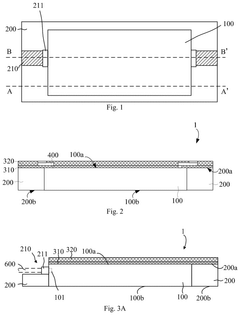
Silicon photonic chip package module based on plastic encapsulation
PatentPendingUS20250291137A1
Innovation
- The proposed silicon photonic chip package module includes a transparent cushioning material layer covering the port of the silicon photonic chip, a plastic encapsulation layer with grooves for fiber optics, and a metal interconnect layer replacing conventional metal wires, allowing direct optical connection to a fiber optic and reducing alignment errors.
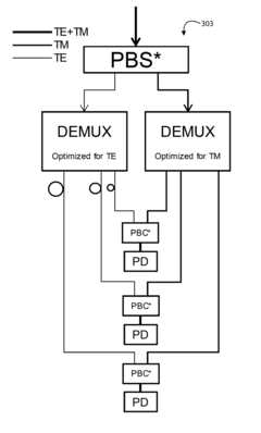
Silicon photonics device and communication system therefor
PatentActiveUS9664854B2
Innovation
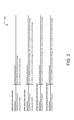
- The use of a 300 nm SOI wafer with a symmetric waveguide structure and polarization compensator materials reduces polarization dependence and sensitivity to thickness changes, enabling improved wavelength stability and transmission efficiency.
Thermal Management Considerations
Thermal management represents a critical challenge in silicon photonics packaging due to the temperature sensitivity of photonic components and the high heat generation in integrated electronic-photonic systems. Silicon photonics devices typically operate optimally within narrow temperature ranges, with performance degradation occurring when thermal conditions deviate from design parameters. The thermal expansion coefficient mismatch between different packaging materials can lead to stress-induced birefringence, wavelength shifts, and coupling efficiency variations that significantly impact device reliability.
Advanced thermal interface materials (TIMs) play a crucial role in silicon photonics packaging by facilitating efficient heat dissipation. Metal-based TIMs, including indium and gold-tin alloys, offer excellent thermal conductivity (40-86 W/m·K) but present challenges regarding cost and processing complexity. Polymer-based TIMs enhanced with ceramic or metallic fillers provide a balance between thermal performance (1-5 W/m·K) and manufacturing compatibility, making them suitable for many commercial applications despite their lower thermal conductivity compared to metal alternatives.
The integration of active cooling solutions has become increasingly important as power densities in silicon photonic circuits continue to rise. Thermoelectric coolers (TECs) incorporated directly into packages enable precise temperature control within ±0.1°C, though they introduce additional power consumption and reliability concerns. Microfluidic cooling channels fabricated within silicon substrates represent an emerging approach, offering localized cooling capabilities with minimal impact on optical performance, achieving thermal resistances below 0.1 K/W in advanced implementations.
Thermal simulation and modeling have become essential tools in the design optimization process for silicon photonics packaging. Finite element analysis enables accurate prediction of temperature distributions and thermal gradients across complex integrated structures. These simulations help identify potential hotspots and guide material selection and geometry optimization before physical prototyping begins, significantly reducing development cycles and improving first-pass design success rates.
Recent advancements in thermally conductive ceramics, including aluminum nitride (AlN) and silicon carbide (SiC), have expanded the material options for silicon photonics packaging. These materials offer thermal conductivities of 170-270 W/m·K while maintaining electrical isolation properties critical for high-frequency applications. Their coefficients of thermal expansion can be engineered to better match silicon, minimizing thermally-induced stress during temperature cycling and improving long-term reliability in harsh operating environments.
The development of heterogeneous integration approaches has introduced additional thermal management complexities that require innovative material solutions. As silicon photonics increasingly incorporates III-V lasers, modulators, and detectors alongside CMOS electronics, the resulting thermal profiles become more complex and demanding. Next-generation thermal management materials, including graphene-enhanced composites and phase-change materials, are being explored to address these challenges while maintaining compatibility with established manufacturing processes.
Supply Chain Resilience and Sustainability
The silicon photonics packaging materials supply chain faces significant vulnerabilities due to its reliance on specialized materials and geographically concentrated manufacturing capabilities. Critical materials such as high-purity silicon wafers, specialized polymers for waveguides, and rare earth elements for optical amplification are often sourced from limited suppliers, creating potential bottlenecks. The COVID-19 pandemic exposed these vulnerabilities, with disruptions in semiconductor manufacturing causing cascading effects throughout the silicon photonics ecosystem.
Building resilience in this supply chain requires multi-faceted approaches. Diversification of supplier networks has emerged as a primary strategy, with leading companies establishing relationships with multiple vendors across different geographic regions. This geographical diversification helps mitigate risks associated with regional disruptions, whether from natural disasters, geopolitical tensions, or public health emergencies. Companies like Intel and GlobalFoundries have pioneered these approaches, investing in alternative sourcing pathways for critical materials.
Vertical integration represents another resilience strategy gaining traction. By controlling more of their supply chain, companies can reduce dependencies on external suppliers. This approach has been particularly effective for specialized packaging materials where alternatives are limited. However, this strategy requires significant capital investment and may not be feasible for smaller market participants.
Sustainability considerations have become increasingly intertwined with supply chain resilience. The manufacturing of silicon photonics packaging materials involves energy-intensive processes and potentially hazardous chemicals. Leading companies are implementing circular economy principles, focusing on materials recovery and recycling. Advanced recycling technologies now allow for the recovery of precious metals and rare earth elements from end-of-life photonic components, reducing dependency on primary resource extraction.
Environmental impact reduction initiatives include transitioning to renewable energy sources for manufacturing facilities and developing water recycling systems to minimize consumption in wafer processing. These sustainability measures not only address environmental concerns but also enhance long-term supply security by reducing dependency on finite resources. Companies implementing these practices have reported improved operational efficiency and reduced exposure to resource price volatility.
Regulatory compliance across global markets presents another dimension of supply chain sustainability. Materials used in silicon photonics packaging must increasingly meet stringent environmental regulations such as RoHS and REACH in Europe, creating additional complexity for global supply chains. Forward-thinking companies are adopting design-for-environment approaches, proactively selecting materials that comply with the most stringent global standards to ensure market access and supply chain flexibility.
Unlock deeper insights with PatSnap Eureka Quick Research — get a full tech report to explore trends and direct your research. Try now!
Generate Your Research Report Instantly with AI Agent
Supercharge your innovation with PatSnap Eureka AI Agent Platform!