Research on Silicon Photonics Packaging and Thermal Stability
SEP 29, 202510 MIN READ
Generate Your Research Report Instantly with AI Agent
Patsnap Eureka helps you evaluate technical feasibility & market potential.
Silicon Photonics Background and Objectives
Silicon photonics has emerged as a transformative technology in the field of integrated photonics, combining the manufacturing advantages of silicon electronics with optical communication capabilities. The evolution of this technology began in the late 1980s with pioneering research on silicon-based optical components, but significant advancements only materialized in the early 2000s when researchers successfully demonstrated high-speed silicon modulators and detectors.
The technology leverages silicon's properties as a semiconductor material with excellent optical characteristics in the infrared spectrum, particularly at the telecommunications wavelengths of 1.3 and 1.55 micrometers. This compatibility with existing CMOS fabrication infrastructure has positioned silicon photonics as a promising solution for addressing the increasing bandwidth demands in data centers, telecommunications, and high-performance computing applications.
Recent years have witnessed an accelerated development trajectory, with the global silicon photonics market expanding at a compound annual growth rate exceeding 20%. This growth is primarily driven by the exponential increase in data traffic, the limitations of traditional electronic interconnects in terms of power consumption and bandwidth, and the need for more efficient data processing architectures.
The packaging and thermal stability aspects of silicon photonics represent critical challenges that must be addressed to enable widespread commercial adoption. Traditional electronic packaging methods are often incompatible with photonic components due to the precise alignment requirements and thermal sensitivity of optical structures. Temperature variations can cause significant wavelength shifts in optical devices, affecting signal integrity and system performance.
The primary technical objectives in silicon photonics packaging and thermal stability research include developing cost-effective packaging solutions that maintain optical alignment across varying environmental conditions, creating thermally compensated designs that minimize wavelength drift, and establishing standardized interfaces between photonic and electronic components. Additionally, there is a focus on improving coupling efficiency between optical fibers and photonic integrated circuits while ensuring scalability for high-volume manufacturing.
Future technological trends point toward the integration of multiple functionalities on a single chip, including optical, electronic, and potentially quantum components. This heterogeneous integration approach aims to overcome the limitations of individual technologies while leveraging their respective strengths. The ultimate goal is to develop a mature silicon photonics platform that enables high-bandwidth, energy-efficient optical communication systems with robust thermal performance across diverse operating environments.
Market Analysis for Silicon Photonics Applications
The silicon photonics market is experiencing robust growth, with a projected CAGR of 23.4% from 2023 to 2030, potentially reaching $9.3 billion by 2030. This remarkable expansion is primarily driven by the increasing demand for high-speed data transmission, cloud computing infrastructure, and the exponential growth in data center traffic worldwide. Silicon photonics technology offers significant advantages in bandwidth, power efficiency, and integration capabilities that position it as a critical enabler for next-generation communication networks.
Data centers represent the largest application segment, accounting for approximately 60% of the current silicon photonics market. The need for higher data rates, reduced power consumption, and increased port density in hyperscale data centers has accelerated adoption of silicon photonics-based transceivers and interconnects. Major cloud service providers including Google, Amazon, and Microsoft have already begun deploying silicon photonics solutions in their infrastructure.
Telecommunications applications constitute the second-largest market segment, with particular growth in metro networks and long-haul communications. The transition to 5G and eventually 6G networks will further drive demand for silicon photonics components that can handle increased bandwidth requirements while maintaining signal integrity over longer distances.
Emerging applications in sensing, LiDAR for autonomous vehicles, and quantum computing are expected to create new market opportunities. The automotive LiDAR segment alone is projected to grow at over 30% annually as autonomous driving technologies mature and gain regulatory approval across major markets.
Regionally, North America currently leads the silicon photonics market with approximately 40% share, followed by Europe and Asia-Pacific. However, the Asia-Pacific region is expected to witness the fastest growth rate due to increasing investments in communication infrastructure, particularly in China, Japan, and South Korea.
The market landscape features both established players and innovative startups. Intel, Cisco, Juniper Networks, and Broadcom represent the established segment, while companies like Ayar Labs, Lightmatter, and SiLC Technologies are driving innovation in specialized applications. Recent strategic acquisitions, such as Marvell's purchase of Inphi and Cisco's acquisition of Acacia Communications, highlight the industry consolidation trend as companies seek to build comprehensive silicon photonics portfolios.
Customer adoption patterns indicate that thermal stability and packaging solutions represent critical decision factors for end-users. Organizations deploying silicon photonics technology consistently cite concerns about thermal management, long-term reliability, and integration complexity as potential barriers to wider implementation. Market research indicates that solutions addressing these challenges could unlock an additional 15-20% of potential market value currently constrained by these technical limitations.
Current Packaging Challenges and Thermal Issues
Silicon photonics packaging faces significant challenges due to the extreme precision requirements and thermal sensitivity of optical components. Current packaging methods struggle with sub-micron alignment tolerances between optical waveguides and external components such as fibers and lasers. This precision must be maintained throughout the device lifetime despite thermal fluctuations, mechanical stresses, and environmental changes. The industry currently lacks standardized, cost-effective packaging solutions that can scale to high-volume manufacturing while maintaining the necessary performance.
Thermal management represents one of the most critical challenges in silicon photonics. The thermo-optic coefficient of silicon (1.86×10^-4 K^-1) causes significant wavelength shifts of approximately 0.1 nm/°C in resonant devices. This thermal sensitivity creates performance instability in applications requiring precise wavelength control, such as WDM systems and optical switches. Additionally, active components like modulators and germanium photodetectors generate heat during operation, creating localized thermal gradients that affect nearby passive components.
Current thermal compensation approaches include active temperature control using integrated heaters and TEC (thermoelectric cooler) systems. However, these solutions significantly increase power consumption, packaging complexity, and overall cost. For example, maintaining temperature stability within ±0.1°C typically requires 1-2W of power per photonic chip, which becomes prohibitive for densely integrated systems with multiple photonic components.
Material interfaces in silicon photonic packages introduce additional thermal challenges. The coefficient of thermal expansion (CTE) mismatch between silicon (2.6 ppm/°C), silica (0.5 ppm/°C), and packaging materials like FR4 (14-17 ppm/°C) creates mechanical stress during temperature cycling. This stress can lead to fiber misalignment, waveguide deformation, and even catastrophic failure at solder joints and adhesive interfaces. Current solutions using compliant adhesives and stress-relief designs add complexity and cost while providing only partial mitigation.
Hermetic packaging, essential for long-term reliability in telecommunications and data center applications, introduces additional thermal considerations. Hermetic seals using metal solders or glass frits require high-temperature processing (250-450°C), which can damage temperature-sensitive components and create residual stresses. Current approaches using lower-temperature bonding techniques often compromise hermeticity or long-term reliability.
The industry is gradually moving toward wafer-level packaging to address these challenges, but significant hurdles remain. Current wafer-level processes struggle with optical coupling efficiency, thermal management across large areas, and testing methodologies. The lack of standardized design rules and process parameters for thermal management in silicon photonics further complicates development efforts and increases time-to-market for new products.
Current Packaging and Thermal Management Solutions
01 Temperature compensation in silicon photonic devices
Various techniques are employed to compensate for temperature-induced variations in silicon photonic devices. These include using materials with negative thermo-optic coefficients to counterbalance silicon's positive coefficient, implementing feedback control systems that actively adjust device parameters based on temperature changes, and designing athermal waveguide structures that maintain optical performance across temperature ranges. These approaches help maintain signal integrity and operational stability in photonic integrated circuits under varying thermal conditions.- Temperature compensation in silicon photonic devices: Silicon photonic devices are sensitive to temperature variations due to the high thermo-optic coefficient of silicon. Various temperature compensation techniques have been developed to maintain thermal stability, including the use of materials with negative thermo-optic coefficients to counterbalance silicon's positive coefficient. These approaches help maintain consistent optical performance across operating temperature ranges, which is crucial for wavelength-sensitive applications like WDM systems.
- Thermally stable waveguide structures: Advanced waveguide designs incorporate specific materials and geometries to enhance thermal stability in silicon photonic circuits. These include athermal waveguides using cladding materials with compensating thermal properties, slot waveguides with thermal-expansion-matched materials, and specialized ridge waveguide structures. These designs minimize wavelength drift and phase changes due to temperature fluctuations, ensuring reliable operation in varying environmental conditions.
- Active thermal management systems: Active thermal management approaches employ integrated heaters, thermoelectric coolers, and feedback control systems to maintain stable operating temperatures in silicon photonic devices. These systems continuously monitor temperature variations and apply compensating heating or cooling to critical components. Advanced implementations include localized thermal isolation structures and efficient heat dissipation pathways to minimize power consumption while maintaining precise temperature control.
- Thermally stable resonator designs: Microring and microdisk resonators in silicon photonics are particularly sensitive to thermal variations, which can shift their resonance wavelengths. Specialized resonator designs incorporate athermal materials, geometric optimizations, and novel coupling mechanisms to minimize thermal sensitivity. These approaches include vernier-effect configurations, coupled-resonator systems with complementary thermal responses, and hybrid material integration to achieve wavelength stability across wide temperature ranges.
- Packaging and integration solutions for thermal stability: Advanced packaging techniques play a crucial role in maintaining thermal stability of silicon photonic devices. These include hermetic sealing with controlled atmospheres, specialized thermal interface materials, and integrated thermal spreaders. Multi-chip integration approaches with optimized thermal pathways help manage heat distribution across complex photonic systems. Additionally, specialized mounting techniques and substrate materials with matched thermal expansion coefficients minimize stress-induced performance variations.
02 Thermal isolation structures for silicon photonics
Thermal isolation structures are integrated into silicon photonic designs to minimize heat transfer between components and reduce thermal crosstalk. These structures include trenches, suspended regions, and specialized materials with low thermal conductivity. By physically separating heat-generating components from temperature-sensitive elements, these isolation techniques improve the overall thermal stability of photonic integrated circuits and enable more reliable operation in varying environmental conditions.Expand Specific Solutions03 Thermally stable materials for silicon photonics
Advanced materials with superior thermal stability characteristics are incorporated into silicon photonic devices. These include specialized cladding materials, thermally stable polymers, and composite structures that maintain their optical and mechanical properties across wide temperature ranges. The integration of these materials helps to reduce thermal expansion mismatches, minimize stress-induced birefringence, and ensure consistent optical performance under thermal fluctuations, thereby enhancing the overall reliability of silicon photonic systems.Expand Specific Solutions04 Active thermal management in silicon photonics
Active thermal management systems are implemented to maintain optimal operating temperatures in silicon photonic devices. These systems include integrated micro-heaters, thermoelectric coolers, and sophisticated thermal sensing networks that provide real-time temperature monitoring. By actively controlling the thermal environment, these approaches enable precise wavelength tuning, reduce thermal drift in resonant structures, and ensure stable operation of temperature-sensitive photonic components across varying environmental conditions.Expand Specific Solutions05 Thermally robust optical coupling designs
Specialized coupling structures are designed to maintain efficient light transfer between components despite thermal variations. These include temperature-insensitive grating couplers, thermally compensated edge couplers, and adaptive coupling mechanisms that adjust to thermal expansion. By ensuring stable optical coupling across temperature ranges, these designs improve signal integrity, reduce insertion loss variations, and enhance the overall thermal stability of silicon photonic interconnects in integrated optical systems.Expand Specific Solutions
Key Industry Players and Ecosystem Analysis
Silicon photonics packaging and thermal stability research is currently in a growth phase, with the market expected to reach significant expansion due to increasing demand for high-speed data transmission and energy-efficient computing solutions. The competitive landscape features established semiconductor giants like Samsung Electronics, TSMC, and GlobalFoundries investing heavily in silicon photonics integration technologies. Research institutions including Naval Research Laboratory, University of California, and Electronics & Telecommunications Research Institute are advancing fundamental thermal management solutions. Companies like Shin-Etsu Chemical and Dow Silicones are developing specialized materials for photonic packaging, while equipment manufacturers such as Canon are focusing on precision assembly technologies. The technology is approaching commercial maturity for data center applications, though challenges in thermal stability and cost-effective packaging solutions remain significant barriers to widespread adoption.
Samsung Electronics Co., Ltd.
Technical Solution: Samsung has developed comprehensive silicon photonics packaging solutions focusing on high-density integration for data center applications. Their approach utilizes a silicon interposer platform that incorporates both electrical and optical through-silicon vias (TSVs) to enable vertical integration of photonic and electronic dies. Samsung's packaging technology employs active alignment systems with closed-loop feedback to achieve coupling efficiencies exceeding 90% between optical fibers and on-chip waveguides. For thermal stability, Samsung implements localized temperature control using integrated micro-Peltier coolers and thermally isolated optical paths. Their waveguide designs incorporate specialized cladding materials with engineered thermal expansion coefficients to minimize temperature-induced phase shifts. Samsung has also pioneered polymer-based optical coupling interfaces that maintain alignment integrity across wide temperature ranges by accommodating differential thermal expansion between package components. Their solutions have demonstrated stable operation across temperature ranges from 0°C to 70°C with wavelength drift below 0.1nm.
Strengths: Vertical integration expertise from memory and logic manufacturing; advanced materials research capabilities; established high-volume manufacturing infrastructure. Weaknesses: Relatively new entrant to silicon photonics compared to some competitors; active thermal management increases power consumption; packaging solutions primarily optimized for their own device ecosystem.
GlobalFoundries U.S., Inc.
Technical Solution: GlobalFoundries has pioneered a monolithic silicon photonics platform called GF Fotonix that combines RF, digital, and optical components on a single chip. Their packaging approach focuses on wafer-level integration to minimize thermal expansion mismatches between optical and electronic components. The company employs passive alignment techniques using precision etched features on silicon to achieve optical coupling with less than 0.5dB insertion loss. For thermal stability, GlobalFoundries implements athermal waveguide designs using silicon nitride and silicon oxynitride materials that exhibit opposite thermo-optic coefficients to silicon, effectively compensating for temperature-induced wavelength shifts. Their packaging solutions incorporate hermetic sealing techniques to protect sensitive optical interfaces from environmental factors while maintaining thermal performance across industrial temperature ranges. The company has demonstrated reliable operation of their packaged photonic devices across temperature variations of over 100°C with minimal performance degradation.
Strengths: Monolithic integration reduces thermal interfaces and simplifies packaging; established 300mm manufacturing capabilities enable cost-effective production; comprehensive design ecosystem with PDKs supporting thermal simulation. Weaknesses: Limited flexibility compared to heterogeneous integration approaches; thermal compensation techniques may restrict optical design options; packaging solutions optimized primarily for datacom rather than broader applications.
Critical Patents and Research in Photonic Packaging
System for stabilizing the temperature sensitivity in photonic circuits comprising thermoelastic optical circuit claddings
PatentInactiveUS20160011368A1
Innovation
- Thermoelastic claddings with negative thermo-optic coefficients, made from materials like jet fuel, ethyl alcohol, and petroleum oil, are used to passively stabilize photonic circuits by adjusting the effective refractive index, eliminating the need for active heating and reducing power consumption.
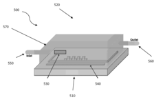
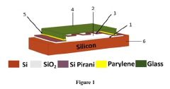
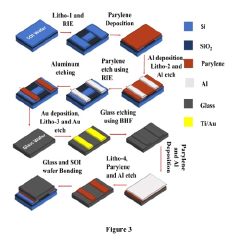
Wafer-wafer bonding using recrystallized parylene material
PatentPendingIN202211071382A
Innovation
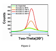
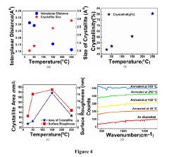
- A low-temperature wafer-wafer vacuum packaging process using recrystallized Parylene material as a bonding layer, subjected to thermal annealing to enhance crystallinity, which forms a hermetic bond between wafers without the need for additional sealing materials or high-temperature processes.
Materials Science Advancements for Photonic Integration
Materials science has emerged as a critical enabler for silicon photonics advancement, particularly in addressing packaging and thermal stability challenges. Recent developments in polymer materials with tailored thermal expansion coefficients have significantly improved the alignment stability between optical components during temperature fluctuations. These specialized polymers maintain dimensional stability across operating temperature ranges of -40°C to 85°C, reducing signal degradation in photonic integrated circuits (PICs).
Novel glass-ceramic composites represent another breakthrough, offering thermal conductivity values approaching 20 W/m·K while maintaining optical transparency. These materials facilitate efficient heat dissipation from active photonic components without compromising optical performance, addressing a fundamental challenge in high-density photonic integration.
Advanced metal alloys with precisely engineered thermal expansion properties have revolutionized hermetic packaging solutions. These alloys, typically incorporating combinations of copper, tungsten, and molybdenum, provide expansion coefficients closely matching silicon substrates (2.6-3.0 ppm/°C), minimizing thermally-induced stress at interface points during temperature cycling.
Thin-film dielectric materials have evolved to offer both optical and thermal functionality. Multi-layer stacks of alternating silicon dioxide and silicon nitride not only serve as optical waveguide cladding but also act as thermal isolation barriers, protecting temperature-sensitive components from heat-generating elements within the same package.
Carbon-based materials, particularly diamond-like carbon (DLC) coatings and graphene-enhanced composites, are emerging as next-generation thermal management solutions. With thermal conductivity exceeding 1000 W/m·K in certain configurations, these materials enable unprecedented heat spreading capabilities while maintaining compatibility with standard semiconductor processing techniques.
Adhesive technology has similarly advanced, with thermally-conductive epoxies achieving bond strengths above 25 MPa while maintaining flexibility across wide temperature ranges. These specialized formulations incorporate ceramic nanoparticles that enhance thermal conductivity without compromising optical transparency or introducing stress points during thermal cycling.
The integration of phase-change materials (PCMs) represents a promising frontier, offering dynamic thermal management through controlled absorption and release of latent heat. These materials can temporarily buffer temperature fluctuations, maintaining stable operating conditions for temperature-sensitive photonic components during transient thermal events.
Manufacturing Scalability and Cost Considerations
The scalability of silicon photonics manufacturing represents a critical factor in the technology's widespread adoption. Current manufacturing processes for silicon photonics devices primarily leverage existing CMOS infrastructure, offering significant advantages in terms of process maturity and equipment availability. However, the specialized packaging requirements for photonic integrated circuits (PICs) present unique challenges that impact production scalability and cost structures.
Traditional semiconductor packaging techniques require substantial modification to accommodate optical interfaces, fiber alignment, and thermal management considerations specific to silicon photonics. The precision required for optical coupling between fibers and on-chip waveguides demands sub-micron alignment accuracy, which significantly increases packaging complexity and associated costs. Industry estimates suggest that packaging can represent 60-80% of the total manufacturing cost for silicon photonic devices, creating a substantial barrier to mass-market adoption.
Automated assembly processes are emerging as a key enabler for manufacturing scalability. Advanced pick-and-place tools with machine vision capabilities have demonstrated promising results in reducing the time and labor costs associated with fiber-chip coupling. Several equipment manufacturers have developed specialized tools capable of achieving the required alignment precision while maintaining throughput rates compatible with volume production. These developments are gradually reducing the packaging cost premium compared to conventional electronic components.
Wafer-level packaging approaches offer another pathway to improved scalability. By performing critical alignment and attachment steps at the wafer level rather than for individual dies, manufacturers can amortize precision handling costs across multiple devices. Recent innovations in wafer-level optical coupling using grating structures and polymer waveguides have shown potential for reducing per-unit costs while maintaining acceptable optical performance characteristics.
Material selection also significantly impacts manufacturing economics. While silicon provides an excellent platform for waveguide structures, the integration of active components often requires hybrid approaches incorporating III-V materials. The bonding processes used for these heterogeneous integrations add complexity and cost to the manufacturing flow. Research into improved bonding techniques and alternative material systems continues to advance, with several promising approaches demonstrating improved yield rates and reduced process complexity.
Supply chain development represents another crucial aspect of manufacturing scalability. The specialized nature of photonic components has historically resulted in fragmented supply chains with limited economies of scale. However, increasing standardization efforts and the emergence of photonic design automation tools are fostering a more cohesive ecosystem. Industry consortia are working to establish common interfaces and process design kits that will enable more efficient collaboration between design houses, foundries, and packaging specialists.
Unlock deeper insights with Patsnap Eureka Quick Research — get a full tech report to explore trends and direct your research. Try now!
Generate Your Research Report Instantly with AI Agent
Supercharge your innovation with Patsnap Eureka AI Agent Platform!