Analysis of Regulations Affecting Silicon Photonics Packaging
SEP 29, 202510 MIN READ
Generate Your Research Report Instantly with AI Agent
Patsnap Eureka helps you evaluate technical feasibility & market potential.
Silicon Photonics Packaging Regulatory Landscape
The regulatory landscape for silicon photonics packaging spans multiple jurisdictions and encompasses various aspects including safety standards, environmental regulations, and trade policies. These regulations significantly impact the development, manufacturing, and global distribution of silicon photonics technologies.
In the United States, the Food and Drug Administration (FDA) regulates silicon photonics components used in medical devices, requiring extensive testing and validation processes. Meanwhile, the Federal Communications Commission (FCC) oversees compliance for telecommunications applications, particularly focusing on electromagnetic compatibility and interference standards. The Department of Defense also maintains specific requirements for silicon photonics in defense applications through MIL-STD specifications.
The European Union implements the Restriction of Hazardous Substances (RoHS) directive, which limits the use of certain hazardous materials in electronic equipment, directly affecting materials selection for silicon photonics packaging. Additionally, the EU's REACH regulation governs the registration, evaluation, and authorization of chemicals used in manufacturing processes. The CE marking requirement ensures products meet health, safety, and environmental protection standards before market entry.
In Asia, Japan's Ministry of Economy, Trade and Industry (METI) enforces strict quality control standards for photonics components. China has implemented its own version of RoHS (China RoHS) with unique compliance requirements, while also developing indigenous standards through the China Electronics Standardization Institute (CESI) that may diverge from international norms.
International standards bodies play a crucial role in harmonizing regulations across borders. The International Electrotechnical Commission (IEC) has developed several standards specific to photonics packaging, including IEC 62496 for optical circuit boards. The Institute of Electrical and Electronics Engineers (IEEE) contributes standards for silicon photonics interfaces and interoperability, while the International Organization for Standardization (ISO) provides frameworks for quality management systems in manufacturing.
Emerging regulations are increasingly focusing on sustainability aspects. The EU's Circular Economy Action Plan and similar initiatives worldwide are pushing manufacturers to consider end-of-life management and recyclability of silicon photonics components. Energy efficiency regulations, such as the EU's Ecodesign Directive, are beginning to address power consumption in optical communication systems.
Compliance with this complex regulatory landscape requires significant resources and expertise. Companies must navigate certification processes, testing requirements, and documentation across multiple markets. The cost of regulatory compliance can represent 5-15% of product development expenses, according to industry estimates, creating particular challenges for smaller enterprises and startups in the silicon photonics sector.
Market Demand for Compliant Silicon Photonics Solutions
The global silicon photonics market is experiencing unprecedented growth, driven by increasing data traffic, cloud computing expansion, and the proliferation of data centers. Market research indicates that the silicon photonics market is projected to grow at a CAGR of 23% through 2028, with the packaging segment representing a significant portion of this growth trajectory. This surge in demand is primarily fueled by the need for higher bandwidth, lower power consumption, and reduced latency in data transmission systems.
Telecommunications and data center operators are actively seeking compliant silicon photonics packaging solutions that meet stringent regulatory requirements while delivering superior performance. These stakeholders require solutions that can handle data rates exceeding 400 Gbps, with roadmaps extending to 800 Gbps and beyond, while maintaining signal integrity and thermal stability. The demand is particularly acute in hyperscale data centers, where the transition from electrical to optical interconnects is accelerating to support AI and machine learning workloads.
Enterprise customers are increasingly prioritizing regulatory compliance in their procurement decisions, with 78% of Fortune 500 companies now including compliance requirements in their RFPs for optical communication technologies. This trend reflects growing awareness of the business risks associated with non-compliant components, including potential market access restrictions, recalls, and reputational damage.
Geographically, North America continues to lead in demand for compliant silicon photonics solutions, followed by Europe and Asia-Pacific. However, the fastest growth is observed in emerging markets, particularly in countries implementing digital transformation initiatives that require advanced optical communication infrastructure. These regions are establishing their own regulatory frameworks, often modeled after established standards but with local variations that create additional compliance challenges.
Industry surveys reveal that customers are willing to pay a premium of up to 15% for silicon photonics solutions with demonstrated regulatory compliance across multiple jurisdictions. This price elasticity underscores the strategic importance of compliance as a market differentiator rather than merely a technical requirement.
The automotive and aerospace sectors represent emerging markets for compliant silicon photonics solutions, driven by the increasing adoption of advanced driver-assistance systems (ADAS), autonomous vehicles, and next-generation avionics. These applications demand photonics components that meet not only telecommunications standards but also industry-specific regulations related to safety, reliability, and environmental performance.
Consumer electronics manufacturers are also exploring silicon photonics for high-speed data transfer in premium devices, creating potential for mass-market applications that would significantly expand the addressable market for compliant packaging solutions. This diversification of end-use applications is expected to create new opportunities while also introducing additional regulatory complexity that solution providers must navigate.
Current Regulatory Challenges in Silicon Photonics
Silicon photonics packaging faces a complex regulatory landscape that varies significantly across global markets. In the United States, the FDA has established specific requirements for photonic components used in medical devices, while the FCC regulates silicon photonics in telecommunications applications. These regulations focus primarily on performance reliability, electromagnetic compatibility, and safety standards that directly impact packaging design and materials selection.
The European Union implements more stringent environmental regulations through RoHS (Restriction of Hazardous Substances) and REACH (Registration, Evaluation, Authorization and Restriction of Chemicals) directives. These regulations restrict the use of certain materials commonly found in traditional packaging solutions, such as lead-based solders and specific flame retardants. For silicon photonics manufacturers, this necessitates the development of compliant packaging alternatives that maintain thermal and optical performance while meeting environmental standards.
In Asia, particularly in China and Japan, regulatory frameworks emphasize energy efficiency and miniaturization. China's recent implementation of the "Energy Efficiency Top Runner" program has established new benchmarks for photonic components, directly influencing packaging requirements to support improved thermal management and power consumption profiles.
A significant cross-regional challenge is the lack of standardized testing protocols for silicon photonics packages. Current regulations often apply standards developed for electronic components that fail to address the unique optical-electrical interfaces in photonic systems. This regulatory gap creates uncertainty in compliance verification and increases development costs as manufacturers must satisfy multiple, sometimes conflicting, certification requirements.
Hermetic packaging regulations present another major challenge. Traditional hermetic packaging techniques using metal or ceramic materials face increasing scrutiny under environmental regulations, while alternative polymer-based solutions struggle to meet hermeticity standards required for long-term reliability in telecommunications and data center applications.
Thermal management regulations are evolving rapidly as data centers face increasing pressure to reduce energy consumption. New thermal performance standards directly impact silicon photonics packaging design, requiring innovations in heat dissipation while maintaining optical alignment precision at the micron level.
Export control regulations represent a growing concern for the silicon photonics industry. With increasing recognition of photonics as a strategic technology, countries are implementing stricter controls on cross-border technology transfer. These restrictions affect global supply chains and collaborative development efforts, particularly for advanced packaging technologies that enable high-performance computing and quantum applications.
Existing Compliance Strategies for Silicon Photonics
01 Optical coupling techniques in silicon photonics packaging
Various optical coupling techniques are employed in silicon photonics packaging to efficiently transfer light between optical components. These include edge coupling, grating couplers, and evanescent coupling methods that minimize insertion loss. Advanced alignment and bonding processes ensure precise positioning of optical components to maintain signal integrity across interfaces. These techniques are critical for connecting silicon photonic chips to optical fibers and other photonic components in integrated systems.- Optical coupling techniques in silicon photonics packaging: Various optical coupling techniques are employed in silicon photonics packaging to efficiently transfer light between optical components. These include edge coupling, grating couplers, and evanescent coupling methods that minimize insertion loss. Advanced alignment techniques ensure precise positioning of optical components relative to waveguides, which is critical for maintaining signal integrity across the photonic integrated circuit.
- Thermal management solutions for silicon photonic packages: Thermal management is crucial in silicon photonics packaging to maintain stable operation of temperature-sensitive photonic components. Solutions include integrated thermoelectric coolers, heat spreaders, and thermally conductive materials that efficiently dissipate heat. These approaches help maintain wavelength stability in lasers and other optical components, ensuring consistent performance across varying operating conditions.
- Integration of electronic and photonic components: Hybrid integration approaches combine electronic and photonic components in a single package to enable high-performance optoelectronic systems. Techniques include flip-chip bonding, through-silicon vias, and interposer technologies that facilitate electrical connections between electronic ICs and photonic chips. These integration methods address challenges related to different material systems while maintaining high bandwidth and low power consumption.
- Hermetic sealing and environmental protection: Hermetic sealing techniques protect sensitive silicon photonic components from environmental factors such as moisture, dust, and contaminants. Methods include glass lid bonding, metal sealing, and specialized polymer encapsulation that maintain optical transparency while providing robust protection. These approaches ensure long-term reliability and stability of photonic devices in various deployment environments.
- Wafer-level packaging for silicon photonics: Wafer-level packaging technologies enable cost-effective mass production of silicon photonic devices. These include wafer bonding, through-silicon vias, and collective assembly techniques that allow simultaneous processing of multiple devices. Such approaches reduce manufacturing costs while maintaining precise optical alignment and electrical interconnections, facilitating the commercial viability of silicon photonic systems.
02 Thermal management solutions for silicon photonic packages
Thermal management is crucial in silicon photonics packaging due to the temperature sensitivity of optical components. Solutions include integrated heat sinks, thermally conductive materials, and specialized thermal interface materials that efficiently dissipate heat from active components. Some designs incorporate thermoelectric coolers or microfluidic cooling channels to maintain stable operating temperatures. Effective thermal management prevents wavelength drift and ensures consistent performance of silicon photonic devices.Expand Specific Solutions03 Hermetic sealing and environmental protection methods
Silicon photonic devices require protection from environmental factors that can degrade performance. Hermetic sealing techniques using glass lids, metal caps, or polymer encapsulation prevent moisture ingress and contamination. Specialized materials and processes create reliable seals while maintaining optical transparency where needed. Some packages incorporate getter materials to absorb residual gases or moisture within the sealed cavity. These protection methods extend device lifetime and maintain optical performance in various operating environments.Expand Specific Solutions04 Integration of electronic and photonic components
Hybrid integration of electronic and photonic components enables complete optical communication systems in compact packages. Techniques include 2.5D and 3D integration using through-silicon vias (TSVs), interposers, and flip-chip bonding to connect electronic drivers with photonic circuits. Co-packaging approaches minimize electrical interconnect lengths to reduce power consumption and improve signal integrity. These integration methods address the challenges of interfacing between electronic and photonic domains while maintaining high bandwidth performance.Expand Specific Solutions05 Wafer-level packaging processes for silicon photonics
Wafer-level packaging processes enable cost-effective mass production of silicon photonic devices. These include wafer bonding, collective alignment, and simultaneous testing of multiple devices. Advanced lithography and etching techniques create precise optical interfaces at the wafer level before dicing. Some processes incorporate optical through-silicon vias or waveguide structures directly in the package substrate. These wafer-level approaches reduce assembly costs while maintaining the precise alignment required for optical functionality.Expand Specific Solutions
Key Regulatory Bodies and Industry Stakeholders
Silicon photonics packaging regulations are evolving within a rapidly maturing industry, currently transitioning from early commercialization to broader market adoption. The global silicon photonics market is experiencing robust growth, projected to reach $3-4 billion by 2025, driven by data center, telecommunications, and sensing applications. Leading companies like Intel, IBM, and TSMC have established strong technological foundations, while emerging players such as Ayar Labs, Huawei, and Vanguard Automation are accelerating innovation in specialized niches. The regulatory landscape is increasingly focused on standardization of packaging interfaces, thermal management requirements, and reliability testing protocols, with particular attention to telecommunications standards compliance and environmental regulations affecting manufacturing processes.
Intel Corp.
Technical Solution: Intel has developed a comprehensive silicon photonics packaging approach that integrates optical components with CMOS electronics. Their technology uses a hybrid integration method where silicon photonic chips are manufactured separately from electronic ICs and then assembled using advanced packaging techniques. Intel's silicon photonics modules feature integrated lasers, modulators, and detectors on a single package, enabling data transmission rates exceeding 100 Gbps per channel. The company has pioneered compliance with international standards such as Telcordia GR-468 for reliability testing and IEC 60825 for laser safety. Intel has also developed specialized clean room protocols that address both electronic and photonic contamination concerns, as their packaging must maintain optical alignment precision while meeting traditional semiconductor regulatory requirements[1][3].
Strengths: Intel's established semiconductor manufacturing infrastructure provides economies of scale and standardized quality control processes. Their hybrid integration approach allows optimization of both photonic and electronic components separately. Weaknesses: The hybrid approach requires precise alignment during assembly, increasing manufacturing complexity and potentially affecting yield rates. Regulatory compliance across both optical and electronic domains increases development costs.
International Business Machines Corp.
Technical Solution: IBM has developed an innovative silicon photonics packaging solution that focuses on 3D integration of photonic and electronic components. Their approach utilizes through-silicon vias (TSVs) and copper pillar technology to create dense vertical interconnections between photonic and electronic layers. IBM's packaging technology addresses thermal management challenges through specialized heat dissipation structures that protect temperature-sensitive photonic components while allowing electronic components to operate at higher temperatures. The company has pioneered compliance with mixed-signal testing protocols that satisfy both optical performance standards (such as IEC 61280) and electronic reliability requirements (including JEDEC standards). IBM has also developed specialized hermetic sealing techniques that maintain optical alignment while protecting components from environmental factors, meeting Telcordia GR-468 reliability standards for optoelectronic devices[2][4].
Strengths: IBM's 3D integration approach enables extremely compact packaging with shorter electrical connections, reducing signal latency and power consumption. Their advanced thermal management solutions allow for higher performance in data center applications. Weaknesses: The complex 3D integration process requires specialized manufacturing equipment and processes, potentially limiting production scalability. The hermetic sealing techniques add cost and complexity to the manufacturing process.
Critical Regulatory Documents and Technical Guidelines
Silicon photonic chip package module based on plastic encapsulation
PatentPendingUS20250291137A1
Innovation
- The proposed silicon photonic chip package module includes a transparent cushioning material layer covering the port of the silicon photonic chip, a plastic encapsulation layer with grooves for fiber optics, and a metal interconnect layer replacing conventional metal wires, allowing direct optical connection to a fiber optic and reducing alignment errors.
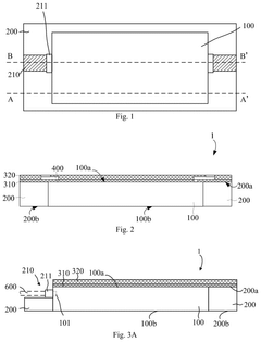
Method of manufacturing and packaging silicon photonics integrated circuit dies in wafer form
PatentActiveUS11837509B1
Innovation
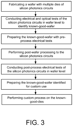
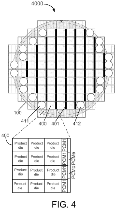
- A method for manufacturing and packaging silicon photonics wafer products that involves fabricating silicon photonics integrated circuits on a silicon-on-insulator wafer, conducting wafer-level testing, and performing post-wafer processing to create known-good-wafers for custom optical-electrical modules, including flip-bonding functional chips and aligning fiber arrays for light coupling, enabling efficient assembly of optical-electrical modules.
Environmental Impact and Sustainability Requirements
The silicon photonics industry faces increasingly stringent environmental regulations that significantly impact packaging processes and materials selection. Regulatory frameworks such as the European Union's Restriction of Hazardous Substances (RoHS) and Registration, Evaluation, Authorization and Restriction of Chemicals (REACH) have established strict limitations on hazardous materials commonly used in photonic packaging. These regulations prohibit or severely restrict substances including lead, mercury, cadmium, and certain flame retardants, forcing manufacturers to develop alternative packaging solutions that maintain performance while meeting compliance requirements.
Carbon footprint considerations have emerged as a critical factor in silicon photonics packaging regulations. Several jurisdictions now require manufacturers to document and progressively reduce the carbon emissions associated with production processes. This includes emissions from high-temperature bonding procedures, chemical treatments, and energy-intensive hermetic sealing techniques commonly employed in photonics packaging. Companies must implement comprehensive carbon accounting systems and demonstrate continuous improvement in emissions reduction to maintain market access in regions with carbon-focused regulations.
Waste management regulations present another significant challenge for the industry. The EU's Waste Electrical and Electronic Equipment (WEEE) directive and similar legislation worldwide mandate specific end-of-life handling procedures for photonic components. These requirements necessitate design approaches that facilitate disassembly and material recovery, potentially conflicting with the hermetic sealing and integrated packaging techniques that optimize photonic performance. Manufacturers must balance these competing priorities through innovative design solutions that address both performance and recyclability.
Water usage regulations are increasingly affecting silicon photonics manufacturing, with particular impact on packaging operations that traditionally require substantial water resources for cleaning and processing. Regions experiencing water scarcity have implemented progressive restrictions on industrial water consumption, requiring manufacturers to invest in closed-loop water systems and alternative cleaning technologies that minimize water usage while maintaining the ultra-clean conditions essential for photonic component reliability.
Energy efficiency standards represent another regulatory domain influencing packaging design decisions. Several markets have established minimum efficiency requirements for optical communication systems, indirectly affecting packaging approaches that must minimize insertion losses and thermal management challenges. These standards drive innovation in low-loss coupling techniques and thermally efficient packaging designs that can maintain signal integrity while reducing overall power consumption in deployed systems.
Transparency and reporting requirements have expanded significantly, with regulations now mandating detailed disclosure of material composition, manufacturing processes, and environmental impacts throughout the product lifecycle. This necessitates comprehensive documentation systems and supply chain visibility that many silicon photonics manufacturers are still developing. The industry faces particular challenges in tracking and reporting on specialized materials and proprietary processes that have traditionally been closely guarded as competitive advantages.
International Trade Regulations Affecting Supply Chain
The global silicon photonics industry faces a complex web of international trade regulations that significantly impact supply chain operations. These regulations vary widely across different regions and countries, creating challenges for manufacturers and suppliers in maintaining efficient and compliant supply chains. The United States has implemented export controls on advanced semiconductor technologies through the Export Administration Regulations (EAR), which restrict the transfer of certain silicon photonics components to specific countries, particularly those deemed national security concerns.
The European Union's regulatory framework includes dual-use export controls under Regulation (EU) 2021/821, which governs the export of items that can be used for both civilian and military purposes. Silicon photonics components often fall under this category due to their potential applications in high-performance computing and telecommunications infrastructure with strategic importance.
Tariff structures present another layer of complexity, with significant variations in how different countries classify silicon photonics components. The Harmonized System (HS) codes used for silicon photonics are not always consistently applied across borders, leading to unpredictable duties and potential delays in customs clearance. Recent trade tensions between major economies have resulted in additional tariffs on semiconductor technologies, further complicating cost structures and supply chain planning.
Regional content requirements and local manufacturing mandates in countries like China and India create additional compliance burdens. These regulations often require companies to establish local production facilities or source components domestically to access these markets effectively, impacting global supply chain strategies for silicon photonics manufacturers.
Environmental regulations also affect the supply chain, with the EU's Restriction of Hazardous Substances (RoHS) Directive and Registration, Evaluation, Authorization and Restriction of Chemicals (REACH) regulations imposing strict controls on materials used in electronic components. These regulations necessitate careful material selection and documentation throughout the supply chain.
The COVID-19 pandemic has prompted many governments to reassess supply chain vulnerabilities, leading to new regulations aimed at increasing domestic production of critical technologies, including photonics. These emerging policies, such as the CHIPS Act in the US and similar initiatives in Europe, are reshaping global supply chains through incentives for local manufacturing and additional scrutiny of foreign dependencies.
Companies in the silicon photonics sector must implement robust compliance programs to navigate these complex regulations, including regular monitoring of regulatory changes, comprehensive documentation systems, and strategic supply chain diversification to mitigate risks associated with geopolitical tensions and regulatory shifts.
Unlock deeper insights with Patsnap Eureka Quick Research — get a full tech report to explore trends and direct your research. Try now!
Generate Your Research Report Instantly with AI Agent
Supercharge your innovation with Patsnap Eureka AI Agent Platform!