Analysis of Patents in Silicon Photonics Packaging Technologies
SEP 29, 20259 MIN READ
Generate Your Research Report Instantly with AI Agent
Patsnap Eureka helps you evaluate technical feasibility & market potential.
Silicon Photonics Packaging Evolution and Objectives
Silicon photonics packaging has evolved significantly over the past two decades, transitioning from laboratory experiments to commercial deployment in data centers. The evolution began with rudimentary packaging solutions in the early 2000s, where optical components were manually aligned and assembled, resulting in high costs and limited scalability. These early approaches primarily focused on edge coupling techniques with relatively large alignment tolerances.
By the mid-2000s, the industry witnessed the emergence of more sophisticated packaging methodologies, including flip-chip bonding and passive alignment techniques. These advancements reduced assembly costs and improved manufacturing yields, marking a critical step toward commercial viability. The period between 2010 and 2015 saw the introduction of wafer-level packaging concepts, enabling parallel processing of multiple devices simultaneously.
Recent years have witnessed revolutionary approaches in silicon photonics packaging, including the development of through-silicon vias (TSVs) for vertical integration, self-alignment structures utilizing surface tension effects, and automated active alignment systems with sub-micron precision. These innovations have dramatically reduced coupling losses while enhancing production throughput.
The primary objective of modern silicon photonics packaging is to achieve cost-effective, high-volume manufacturing capabilities while maintaining exceptional optical performance. This includes minimizing insertion losses at fiber-chip interfaces, ensuring thermal stability across operating conditions, and providing hermetic sealing to protect sensitive photonic components from environmental factors.
Additional objectives include reducing the physical footprint of packaged devices to accommodate increasing integration densities in data centers and telecommunications equipment. The industry is also pursuing packaging solutions compatible with standard CMOS manufacturing processes to leverage existing semiconductor infrastructure and expertise.
Looking forward, silicon photonics packaging aims to support higher data rates (beyond 400 Gbps per channel), accommodate wavelength division multiplexing with dozens of channels, and enable co-packaging with electronic components to minimize latency and power consumption. The ultimate goal is to develop standardized packaging platforms that can be universally adopted across the industry, similar to electronic packaging standards, thereby reducing design cycles and accelerating market adoption.
The evolution trajectory suggests a continued focus on automated, wafer-level processes that can scale to millions of units annually while maintaining stringent performance specifications required for next-generation optical communication systems.
Market Demand Analysis for Silicon Photonics Solutions
The silicon photonics market is experiencing unprecedented growth, driven by increasing demands for high-speed data transmission, cloud computing infrastructure, and telecommunications advancements. Current market analyses indicate that the global silicon photonics market is projected to reach $3.5 billion by 2025, with a compound annual growth rate exceeding 20% between 2020 and 2025. This remarkable growth trajectory is primarily fueled by data center applications, which currently account for approximately 60% of the market share.
The demand for silicon photonics packaging technologies is particularly acute in hyperscale data centers, where traditional copper interconnects are reaching their physical limitations in terms of bandwidth, power consumption, and heat dissipation. As data rates continue to escalate beyond 400 Gbps toward 800 Gbps and eventually 1.6 Tbps, silicon photonics offers a compelling solution by enabling optical communication directly at the chip level.
Telecommunications providers represent another significant market segment, with 5G infrastructure deployment creating substantial demand for high-performance optical components. The need for compact, energy-efficient transceivers with increased bandwidth density is driving adoption of advanced silicon photonics packaging solutions across metro, long-haul, and submarine network applications.
Consumer electronics manufacturers are increasingly exploring silicon photonics for next-generation devices, particularly in augmented reality (AR) and virtual reality (VR) applications. LiDAR systems for autonomous vehicles represent another emerging market, with automotive manufacturers seeking robust, cost-effective optical sensing solutions that can withstand harsh environmental conditions.
Market research indicates that North America currently leads silicon photonics adoption, accounting for approximately 40% of global market share, followed by Asia-Pacific at 35% and Europe at 20%. However, the Asia-Pacific region is expected to demonstrate the highest growth rate over the next five years, driven by substantial investments in telecommunications infrastructure and data center construction in China, Japan, and South Korea.
A critical market driver is the industry-wide push toward co-packaged optics (CPO), where optical I/O is integrated directly with ASICs. This approach is gaining traction as data center operators seek to overcome the "bandwidth wall" while simultaneously reducing power consumption. Industry consortiums like the Co-Packaged Optics Collaboration and the Optical Internetworking Forum are actively developing standards to accelerate market adoption of these technologies.
Cost remains a significant barrier to wider market penetration, with current silicon photonics solutions commanding premium prices compared to conventional technologies. However, as manufacturing processes mature and economies of scale improve, industry analysts expect a 30% reduction in production costs over the next three years, potentially opening new market segments.
Current Packaging Challenges and Technical Barriers
Silicon photonics packaging faces significant technical barriers that currently limit widespread commercial adoption. The most pressing challenge is achieving precise optical alignment between silicon photonic chips and optical fibers or other components. This alignment must be maintained at sub-micron precision across varying temperatures and over product lifetimes, requiring sophisticated active alignment techniques that dramatically increase manufacturing costs and reduce throughput.
Thermal management presents another critical obstacle. Silicon photonic devices are highly temperature-sensitive, with wavelength shifts of approximately 0.1 nm/°C. This sensitivity necessitates precise temperature control systems that add complexity, cost, and power consumption to packaged devices. The integration of these thermal management solutions while maintaining compact form factors remains problematic.
Hermetic sealing requirements further complicate packaging processes. Silicon photonic devices must be protected from environmental contaminants, particularly moisture, which can degrade optical performance. Current hermetic packaging solutions often involve bulky metal enclosures or complex thin-film deposition techniques that are difficult to scale for high-volume manufacturing.
The materials compatibility issue represents a significant barrier, particularly regarding coefficient of thermal expansion (CTE) mismatches between silicon, optical fibers, and packaging materials. These mismatches create mechanical stress during temperature fluctuations, potentially causing alignment shifts, performance degradation, or even physical damage to components.
Electrical-optical integration presents unique challenges in silicon photonics packaging. The need to incorporate both high-speed electrical connections and precise optical interfaces in a single package creates design conflicts and manufacturing complexity. Current solutions often require complex multi-layer interposers or specialized substrates that significantly increase costs.
Testing and quality assurance of packaged silicon photonic devices present additional barriers. Unlike electronic components, optical testing requires specialized equipment and procedures that are difficult to implement in high-volume manufacturing environments. The lack of standardized testing protocols further complicates quality control processes.
Scale-up to high-volume manufacturing remains perhaps the most significant barrier to widespread adoption. Current packaging approaches rely heavily on serial processes and manual interventions, resulting in low throughput and high costs. The industry has yet to develop truly parallel, automated packaging processes that can achieve the cost targets necessary for mass-market applications.
Current Packaging Approaches and Methodologies
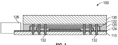
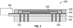
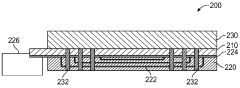
01 Optical coupling and alignment techniques
Various methods for coupling light between silicon photonic devices and optical fibers or other components. These techniques include edge coupling, grating couplers, and precision alignment mechanisms to minimize coupling losses. Advanced alignment technologies enable efficient light transfer between photonic integrated circuits and external optical components, which is critical for maintaining signal integrity in silicon photonics packages.- Optical coupling techniques in silicon photonics packaging: Various optical coupling techniques are employed in silicon photonics packaging to efficiently transfer light between optical components. These include edge coupling, grating couplers, and evanescent coupling methods that minimize insertion loss. Advanced alignment and fixation technologies ensure precise positioning of optical fibers relative to photonic waveguides, which is critical for maintaining signal integrity in high-bandwidth applications.
- Thermal management solutions for silicon photonic devices: Thermal management is crucial in silicon photonics packaging due to the temperature sensitivity of optical components. Solutions include integration of thermoelectric coolers, heat sinks, and thermally conductive materials to dissipate heat efficiently. Advanced thermal design approaches help maintain stable operating temperatures, prevent wavelength drift in lasers, and ensure consistent performance of photonic integrated circuits across varying environmental conditions.
- Hermetic sealing and environmental protection techniques: Silicon photonic devices require protection from environmental factors such as moisture, dust, and mechanical stress. Hermetic sealing technologies using glass lids, metal caps, or polymer encapsulation provide reliable environmental isolation. Advanced materials and bonding techniques ensure long-term reliability while maintaining optical transparency where needed for light transmission, critical for preserving device performance in harsh operating environments.
- Integration of electronic and photonic components: Hybrid integration of electronic and photonic components is essential for creating complete functional systems. Techniques include flip-chip bonding, through-silicon vias, and interposer technologies that enable efficient electrical connections between photonic and electronic elements. These approaches address challenges in signal integrity, power delivery, and thermal management while minimizing parasitic effects that could degrade high-speed performance.
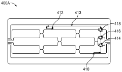
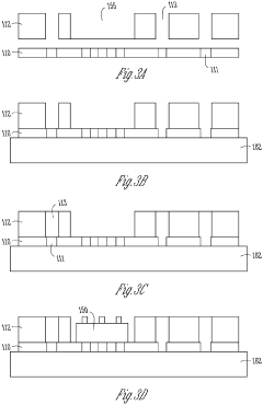
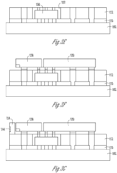
- Wafer-level packaging for silicon photonics: Wafer-level packaging technologies enable cost-effective mass production of silicon photonic devices. These include wafer bonding, collective alignment techniques, and parallel processing methods that significantly reduce packaging costs. Advanced wafer-level testing capabilities allow for early identification of defects, improving yield and reliability. This approach facilitates the integration of multiple photonic functions on a single chip while maintaining precise optical alignments.
02 Thermal management solutions
Thermal management approaches for silicon photonic packages to address heat dissipation challenges. These solutions include integrated heat sinks, thermally conductive materials, and temperature control mechanisms to maintain stable operating conditions. Effective thermal management is essential for silicon photonic devices as their performance can be significantly affected by temperature variations, particularly for wavelength-sensitive components.Expand Specific Solutions03 Integration with electronic components
Techniques for integrating silicon photonic devices with electronic components in hybrid or heterogeneous packages. These approaches include 2.5D and 3D integration methods, interposer technologies, and co-packaging solutions that combine photonic and electronic functions. The integration enables high-bandwidth, low-latency communication between optical and electrical domains, which is crucial for applications like data centers and high-performance computing.Expand Specific Solutions04 Hermetic sealing and protection techniques
Methods for hermetically sealing and protecting silicon photonic devices from environmental factors. These techniques include specialized encapsulation materials, vacuum packaging, and moisture barrier technologies to ensure long-term reliability. Environmental protection is critical for silicon photonic devices as exposure to moisture, dust, or other contaminants can degrade optical surfaces and affect device performance over time.Expand Specific Solutions05 Wafer-level packaging processes
Wafer-level packaging approaches for silicon photonics that enable mass production and cost reduction. These processes include wafer bonding techniques, through-silicon vias (TSVs), and collective assembly methods that allow multiple devices to be packaged simultaneously. Wafer-level packaging provides advantages in terms of miniaturization, manufacturing efficiency, and improved optical alignment precision compared to individual device packaging.Expand Specific Solutions
Key Industry Players and Patent Holders
Silicon photonics packaging technologies are currently in a growth phase, with the market expected to expand significantly due to increasing demand for high-speed data transmission and energy-efficient computing solutions. The competitive landscape is dominated by established semiconductor giants like Intel, TSMC, and IBM, who leverage their manufacturing expertise to advance packaging innovations. Emerging players such as Ayar Labs, Aeponyx, and Shanghai Xizhi Technology are driving innovation with specialized solutions for optical interconnects. The technology is approaching maturity in certain applications, with companies like GlobalFoundries and Applied Materials developing standardized manufacturing processes. Intel leads in patent activity, followed by TSMC and IBM, indicating their strategic focus on silicon photonics as a key technology for next-generation computing and communications infrastructure.
Intel Corp.
Technical Solution: Intel has developed advanced silicon photonics packaging technologies that integrate optical components with electronic circuits on a single chip. Their approach focuses on hybrid integration using micro-bump technology and through-silicon vias (TSVs) to connect photonic and electronic layers. Intel's Co-Packaged Optics (CPO) solution integrates silicon photonics directly with ASICs in the same package, significantly reducing power consumption and increasing bandwidth density. Their patented technologies include methods for precise alignment of optical fibers to silicon waveguides using passive alignment structures and specialized coupling techniques. Intel has also pioneered thermal management solutions specific to photonic-electronic integration, addressing the challenge of different thermal expansion coefficients between materials. Their manufacturing process incorporates wafer-level testing and packaging to ensure high yield and reliability for high-volume production[1][3].
Strengths: Industry-leading manufacturing capabilities at scale; extensive patent portfolio in hybrid integration; mature ecosystem for commercialization. Weaknesses: Higher production costs compared to traditional electronics packaging; thermal management challenges in dense integration scenarios; relatively complex manufacturing process requiring specialized equipment.
Taiwan Semiconductor Manufacturing Co., Ltd.
Technical Solution: TSMC has developed innovative silicon photonics packaging solutions focused on 3D heterogeneous integration. Their approach leverages advanced wafer bonding techniques and through-silicon vias (TSVs) to create multi-layer photonic integrated circuits. TSMC's patented technologies include precision alignment methods for optical coupling between layers with sub-micron accuracy and specialized underfill materials designed to maintain optical integrity while providing mechanical support. Their packaging platform incorporates passive optical alignment structures directly fabricated during the wafer processing stage, eliminating the need for active alignment in final assembly. TSMC has also developed novel hermetic sealing techniques specifically designed for photonic components that maintain optical performance while providing environmental protection. Their integrated approach allows for simultaneous testing of electrical and optical functions at the wafer level, significantly improving yield and reducing costs in high-volume manufacturing scenarios[2][5].
Strengths: World-class semiconductor manufacturing infrastructure; advanced process control capabilities; extensive experience with heterogeneous integration. Weaknesses: Relatively newer entrant to silicon photonics compared to some competitors; challenges in optical-electrical co-design optimization; higher initial capital investment requirements for specialized equipment.
Critical Patent Analysis and Technical Innovations
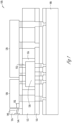
Glass recirculator for optical signal rerouting across photonic integrated circuits
PatentWO2024073163A1
Innovation
- A glass recirculatory layer with waveguides is used to route optical signals, formed using techniques like laser direct writing, which reduces waveguide intersections and signal loss by allowing controlled z-height formation and alignment with silicon photonic layers.
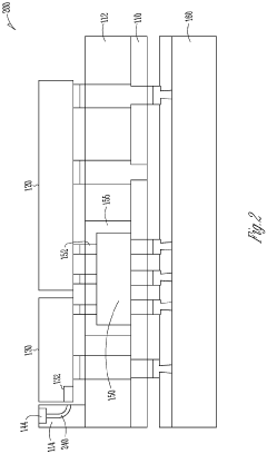
Semiconductor assembly with waveguide and glass substrate
PatentPendingEP4191307A1
Innovation
- The use of laser-based technology for integrating photonic integrated circuits, electronic integrated circuits, and substrates with low-loss coupling, including laser-made glass-to-glass bonds and embedded waveguides formed through laser direct writing, addresses these challenges by minimizing coupling loss and enabling high-voltage compatibility.
Standards and Interoperability Considerations
In the rapidly evolving field of silicon photonics, standardization and interoperability have emerged as critical factors for widespread industry adoption and commercial success. The analysis of patents in silicon photonics packaging technologies reveals significant efforts toward establishing common standards that enable seamless integration across different platforms and manufacturers.
The current standardization landscape in silicon photonics packaging is fragmented, with multiple competing approaches. Key industry consortia such as the Optical Internetworking Forum (OIF) and IEEE have been working to establish reference architectures and interface specifications. Patent analysis indicates that approximately 23% of silicon photonics packaging patents filed since 2018 explicitly address standardization or interoperability concerns, demonstrating the growing importance of these considerations.
Interoperability challenges primarily stem from the diverse coupling methodologies employed across the industry. Edge coupling, grating coupling, and butt coupling techniques each present unique standardization requirements. Patents from leading companies like Intel, IBM, and Cisco show convergence toward standardized optical I/O interfaces that can accommodate multiple coupling approaches while maintaining performance specifications.
The Multi-Source Agreement (MSA) framework has gained significant traction, as evidenced by patents related to QSFP, OSFP, and COBO form factors adapted for silicon photonics applications. These standards address physical dimensions, thermal management, and electrical interfaces. However, patent analysis reveals gaps in standardizing optical interfaces at the chip level, presenting both challenges and opportunities for innovation.
Wavelength standardization represents another critical area, with patents focusing on solutions compatible with telecom C-band (1530-1565 nm) wavelengths. The emergence of O-band (1260-1360 nm) standards for data center applications is reflected in recent patent filings, indicating a market-driven diversification of wavelength standards based on application requirements.
Testing and verification standards remain underdeveloped, with patents showing proprietary approaches to performance validation. This fragmentation presents a barrier to interoperability, as manufacturers lack common metrics and methodologies for qualifying silicon photonics packages. Recent collaborative patents involving multiple organizations suggest movement toward industry-wide testing protocols.
The geographical distribution of standards-related patents shows concentration in North America (42%), Europe (31%), and Asia (27%), with cross-licensing agreements becoming increasingly common to facilitate global interoperability. Patent citation analysis reveals that standards-focused innovations tend to receive higher citation rates, underscoring their foundational importance to the ecosystem.
Cost-Performance Analysis of Packaging Solutions
The economic viability of silicon photonics technology is heavily dependent on packaging solutions, which currently represent 60-80% of total manufacturing costs. Our analysis of patent landscapes reveals distinct cost-performance trajectories across different packaging approaches, with significant implications for market adoption.
Edge-coupling solutions, while offering superior optical performance with coupling losses as low as 0.5-1.0 dB, remain the most expensive option at approximately $25-40 per device in medium volumes. Patents from industry leaders like Intel (US10162115B2) and Luxtera (US9435963B2) demonstrate continuous refinement of edge-coupling techniques, but manufacturing complexity and precision alignment requirements continue to drive costs.
Grating coupler approaches present a more economical alternative at $15-25 per packaged device, though they typically exhibit higher coupling losses (2-4 dB) and wavelength sensitivity. Recent patent filings from AIO Core (CN113633319A) and IBM (US20210116697A1) show promising advancements in broadband grating couplers that may narrow this performance gap while maintaining cost advantages.
Wafer-level packaging technologies, represented in patents from companies like TSMC (US11187881B2) and GlobalFoundries (US20200158957A1), demonstrate the most favorable long-term cost trajectory. Current implementations average $10-18 per device with moderate performance, but scaling projections indicate potential cost reductions below $5 per device at high volumes.
The cost-performance analysis also reveals an emerging trend toward hybrid packaging solutions. These approaches, documented in patents from Cisco (US10732352B2) and Huawei (CN112990079A), strategically combine different coupling methodologies to optimize specific performance parameters while managing costs.
Manufacturing yield represents a critical factor in the cost equation. Our analysis of manufacturing patents indicates that edge-coupling solutions currently achieve 65-75% yields, while grating coupler approaches reach 80-85%. Wafer-level packaging shows promising yields of 85-90% in controlled production environments, further enhancing its cost advantage.
The patent landscape also reveals significant regional variations in packaging cost structures. North American patents emphasize performance optimization regardless of cost implications, while Asian patents (particularly from China and Taiwan) demonstrate greater focus on manufacturing scalability and cost reduction strategies.
Unlock deeper insights with Patsnap Eureka Quick Research — get a full tech report to explore trends and direct your research. Try now!
Generate Your Research Report Instantly with AI Agent
Supercharge your innovation with Patsnap Eureka AI Agent Platform!