Research on Silicone Coatings for Silicon Photonics Packaging
SEP 29, 20259 MIN READ
Generate Your Research Report Instantly with AI Agent
Patsnap Eureka helps you evaluate technical feasibility & market potential.
Silicon Photonics Coating Background & Objectives
Silicon photonics has emerged as a transformative technology in the field of integrated photonics over the past two decades. This technology leverages the mature silicon semiconductor manufacturing infrastructure to create photonic integrated circuits (PICs) that manipulate light for various applications including telecommunications, data centers, sensing, and quantum computing. The evolution of silicon photonics has been driven by the increasing demand for higher bandwidth, lower power consumption, and more compact photonic solutions.
Silicone coatings represent a critical component in silicon photonics packaging, serving as protective layers that shield sensitive optical components from environmental factors while maintaining optical performance. Historically, these coatings have evolved from simple encapsulants to sophisticated materials engineered for specific optical, mechanical, and thermal properties. The progression has been marked by continuous improvements in transparency, refractive index control, adhesion strength, and long-term reliability.
The current technological trajectory points toward developing advanced silicone coating materials that can withstand increasingly demanding operational conditions while providing enhanced functionality. These include coatings with ultra-low optical loss, controlled refractive indices, resistance to high temperatures, and compatibility with automated manufacturing processes. Additionally, there is growing interest in coatings that can enable active functionalities such as tunable optical properties or self-healing capabilities.
The primary objectives of this research are to comprehensively evaluate the state-of-the-art in silicone coating technologies for silicon photonics packaging, identify key performance parameters and limitations of current solutions, and explore innovative approaches to overcome existing challenges. Specifically, we aim to investigate novel silicone formulations that offer superior optical transparency in the relevant wavelength ranges (typically 1310nm and 1550nm), enhanced thermal stability for high-power applications, and improved adhesion to various substrate materials used in photonic packages.
Furthermore, this research seeks to establish correlations between coating composition, processing methods, and resulting performance characteristics. By understanding these relationships, we can develop predictive models that accelerate the development of next-generation coating solutions. The ultimate goal is to enable silicon photonic devices with improved reliability, extended lifetime, and enhanced performance across diverse operating environments.
This investigation also aims to address emerging requirements in the field, such as coatings compatible with heterogeneous integration approaches, environmentally friendly formulations that comply with increasingly stringent regulations, and cost-effective solutions that can facilitate broader commercial adoption of silicon photonics technology.
Market Analysis for Silicone-Coated Photonic Devices
The global market for silicone-coated photonic devices is experiencing robust growth, driven by increasing demand for high-speed data transmission and processing capabilities across multiple industries. Current market valuations indicate that silicon photonics technology is projected to grow at a compound annual growth rate of 23% through 2027, with the packaging segment representing approximately 30% of the total market value.
Silicone coatings specifically address critical protection needs in photonic integrated circuits, offering enhanced reliability in diverse operating environments. Market research shows that telecommunications and data center applications currently dominate demand, accounting for over 60% of market share, while emerging applications in automotive LiDAR, medical diagnostics, and quantum computing are rapidly expanding adoption.
Consumer electronics manufacturers are increasingly incorporating silicon photonics into next-generation devices, creating substantial market pull for advanced packaging solutions that can withstand consumer use conditions. This trend is particularly evident in the smartphone and wearable technology segments, where miniaturization and durability requirements are stringent.
Regional analysis reveals that North America currently leads market consumption of silicone-coated photonic devices, followed closely by Asia-Pacific. However, the fastest growth is occurring in the Asia-Pacific region, particularly in China, Taiwan, and Singapore, where significant investments in manufacturing infrastructure are expanding production capacity.
Market segmentation by coating type shows that optically transparent silicones with controlled refractive indices command premium pricing, with specialized formulations for specific wavelength ranges gaining traction. The market for UV-curable silicones is growing particularly fast due to manufacturing efficiency advantages.
Customer requirements analysis indicates increasing demand for silicone coatings that can withstand wider temperature ranges (-65°C to 200°C) while maintaining optical clarity and mechanical stability. Additionally, environmental regulations are driving interest in halogen-free formulations that comply with RoHS and REACH standards.
Price sensitivity varies significantly by application segment. While telecommunications providers prioritize long-term reliability over initial cost, consumer electronics manufacturers are more price-sensitive and seek cost-effective solutions for high-volume production. This market dynamic is creating opportunities for tiered product offerings with different performance-to-price ratios.
Supply chain analysis reveals potential vulnerabilities in raw material sourcing for specialty silicones, with several key components facing periodic supply constraints. This situation presents both a challenge and an opportunity for companies able to secure reliable material sources or develop alternative formulations.
Current Challenges in Silicon Photonics Packaging
Silicon photonics packaging represents a critical bottleneck in the commercialization and widespread adoption of silicon photonics technology. Despite significant advancements in silicon photonic device design and fabrication, packaging challenges continue to impede cost-effective, high-volume manufacturing and reliable field deployment. The integration of optical components with electronic systems introduces unique challenges that conventional electronic packaging approaches cannot adequately address.
Thermal management remains one of the most significant challenges in silicon photonics packaging. Silicon photonic devices are highly temperature-sensitive, with wavelength shifts of approximately 0.1 nm/°C for resonant structures. This sensitivity necessitates precise temperature control or compensation mechanisms to maintain optical performance across varying operating conditions. Current thermal management solutions add complexity and cost to packaging processes.
Optical coupling efficiency between fiber optics and silicon waveguides presents another major hurdle. The mode size mismatch between standard single-mode fibers (approximately 10 μm) and silicon waveguides (typically 0.2-0.5 μm) results in significant coupling losses. While various coupling techniques exist, including edge coupling, grating couplers, and spot-size converters, each introduces trade-offs between bandwidth, polarization sensitivity, alignment tolerance, and manufacturing complexity.
Hermetic sealing requirements further complicate packaging solutions. Silicon photonic devices must be protected from environmental contaminants, particularly moisture, which can degrade optical performance over time. Traditional hermetic packaging approaches using metal or ceramic housings are often bulky and expensive, contradicting the miniaturization advantages of silicon photonics.
Alignment precision during assembly poses exceptional challenges. Sub-micron alignment accuracy is typically required between optical components, necessitating specialized equipment and processes. Active alignment techniques, while effective, are time-consuming and costly for high-volume manufacturing scenarios. Passive alignment alternatives often sacrifice coupling efficiency for manufacturing simplicity.
Material compatibility issues arise when integrating diverse materials within a single package. Coefficient of thermal expansion (CTE) mismatches between silicon, polymers, metals, and ceramics can induce stress and lead to misalignment or device failure during thermal cycling. Additionally, outgassing from packaging materials can contaminate optical surfaces, degrading performance over time.
Scalability to high-volume manufacturing represents perhaps the most pressing challenge. Current packaging approaches often rely on serial processes with significant manual intervention, resulting in high costs and limited throughput. The industry lacks standardized packaging platforms and processes comparable to those established in electronic packaging, hampering economies of scale.
Current Silicone Coating Solutions
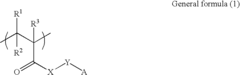
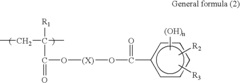
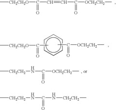
01 Silicone coating compositions and formulations
Various silicone coating compositions have been developed with specific formulations to enhance performance characteristics. These compositions typically include silicone polymers, crosslinking agents, and additives that provide desired properties such as adhesion, durability, and flexibility. The formulations may incorporate different types of silicones including polydimethylsiloxanes, fluorosilicones, or silicone resins, which can be tailored for specific applications and substrates.- Silicone coating compositions for improved durability: Silicone coating compositions can be formulated to provide enhanced durability and weather resistance. These compositions typically include silicone polymers with specific functional groups that improve adhesion to substrates and resistance to environmental factors. The coatings can be designed to withstand UV radiation, temperature fluctuations, and chemical exposure, making them suitable for outdoor applications and protective finishes.
- Water-repellent silicone coatings: Silicone coatings can be formulated to provide excellent water repellency and hydrophobic properties. These coatings typically contain silicone resins or oils that create a barrier against moisture penetration. The hydrophobic nature of these coatings makes them ideal for applications requiring water resistance, such as building materials, textiles, and electronic components. These coatings can also provide protection against corrosion and water damage.
- Heat-resistant silicone coating systems: Specialized silicone coating formulations can be developed to withstand extreme temperatures and thermal cycling. These heat-resistant coatings typically incorporate silicone polymers with high thermal stability and may include additives such as metal oxides or ceramic fillers to enhance temperature resistance. Applications include industrial equipment, automotive components, and cookware that are exposed to high temperatures. These coatings maintain their protective properties even under thermal stress.
- Silicone coatings with enhanced adhesion properties: Silicone coatings can be modified to improve adhesion to various substrates including metals, plastics, and glass. These formulations often incorporate adhesion promoters, coupling agents, or surface treatments to enhance bonding. The improved adhesion properties ensure coating durability and longevity even under challenging conditions. These coatings can be designed for specific substrate compatibility while maintaining the beneficial properties of silicones.
- Environmentally friendly silicone coating technologies: Recent developments in silicone coating technology have focused on creating more environmentally friendly formulations with reduced VOC content and elimination of harmful components. These eco-friendly coatings may use water-based systems, solvent-free approaches, or bio-based ingredients while maintaining performance characteristics. The environmentally conscious formulations address regulatory requirements and sustainability concerns while providing the protective and functional benefits expected from silicone coatings.
02 Weatherproof and protective silicone coatings
Silicone coatings are widely used for weatherproofing and protection of various surfaces. These coatings provide excellent resistance to UV radiation, extreme temperatures, moisture, and environmental pollutants. The protective properties of silicone coatings make them suitable for applications in construction, automotive, and marine industries where surfaces are exposed to harsh environmental conditions. These coatings typically offer long-term durability and maintain their protective properties over extended periods.Expand Specific Solutions03 Application methods for silicone coatings
Various methods have been developed for applying silicone coatings to different substrates. These include spray coating, dip coating, roll coating, and brush application techniques. The application method can significantly impact the coating thickness, uniformity, and adhesion properties. Some advanced application techniques involve specialized equipment for precise control of coating parameters. The curing process following application is also critical, with options including thermal curing, moisture curing, or radiation curing depending on the coating formulation.Expand Specific Solutions04 Silicone coatings with enhanced properties
Specialized silicone coatings have been developed with enhanced properties such as improved adhesion, abrasion resistance, chemical resistance, and thermal stability. These enhanced properties are achieved through the incorporation of functional additives, nanoparticles, or through chemical modification of the silicone polymers. Some formulations include hybrid systems that combine silicones with other materials like polyurethanes or epoxies to achieve synergistic performance benefits. These enhanced coatings address specific challenges in demanding applications.Expand Specific Solutions05 Industrial applications of silicone coatings
Silicone coatings find widespread use across various industries including electronics, automotive, aerospace, construction, and medical devices. In electronics, they provide insulation and protection against moisture and contaminants. In automotive and aerospace applications, they offer heat resistance and durability. For construction, they provide water repellency and weather resistance. Medical applications utilize biocompatible silicone coatings for implantable devices. The versatility of silicone coatings makes them suitable for numerous specialized industrial applications.Expand Specific Solutions
Leading Companies in Silicon Photonics Packaging
The silicon photonics packaging coatings market is currently in a growth phase, with an estimated market size of $300-500 million and projected annual growth of 25-30%. The technology maturity varies across applications, with telecommunications being more advanced than emerging quantum computing implementations. Leading players include Taiwan Semiconductor Manufacturing Co., which has integrated silicon photonics into its advanced packaging solutions, and IBM Research, which has pioneered silicone coating technologies for thermal management. Shin-Etsu Chemical and Momentive Performance Materials dominate the specialized silicone materials supply chain, while Intel and II-VI Delaware are advancing integration techniques. Academic-industry partnerships, particularly involving Brown University and Centre National de la Recherche Scientifique, are accelerating innovation in hermetic sealing and environmental protection solutions.
Taiwan Semiconductor Manufacturing Co., Ltd.
Technical Solution: TSMC has developed advanced silicone coating solutions for silicon photonics packaging that focus on low-loss optical interfaces. Their approach utilizes specialized silicone materials with controlled refractive indices to minimize coupling losses at fiber-chip interfaces. TSMC's silicone coatings incorporate nano-silica fillers to enhance thermal stability while maintaining optical transparency in the relevant wavelength ranges (1310nm and 1550nm). The company has implemented a proprietary curing process that minimizes stress-induced birefringence, which is critical for maintaining signal integrity in polarization-sensitive photonic circuits[1]. Their packaging technology includes hermetic sealing techniques using silicone-based materials that provide protection against moisture while allowing for thermal expansion coefficient matching between different package components[3].
Strengths: Superior optical transparency in telecom wavelengths and excellent thermal stability across wide temperature ranges (-40°C to 125°C). The coatings demonstrate exceptional adhesion to both silicon and glass surfaces, enabling reliable packaging solutions. Weaknesses: Higher manufacturing costs compared to traditional packaging methods and limited scalability for very high-volume production environments.
International Business Machines Corp.
Technical Solution: IBM has pioneered silicone coating technology for silicon photonics packaging through their "optical cushion" approach. This involves applying specially formulated silicone materials that serve as both optical coupling media and mechanical buffers between photonic chips and optical fibers. IBM's silicone formulations feature customized viscosity profiles that enable precise deposition using automated equipment, with thickness control within ±2μm[2]. The company has developed UV-curable silicone variants that allow for rapid processing while maintaining optical clarity. Their coatings incorporate proprietary additives that enhance long-term stability against yellowing and refractive index drift, which are common challenges in optical applications[4]. IBM's packaging solution includes silicone-based edge couplers that achieve coupling losses below 1dB per facet across the C-band spectrum, representing significant improvement over conventional approaches[5].
Strengths: Exceptional optical coupling efficiency with demonstrated insertion losses below 1dB. The technology offers excellent mechanical protection against thermal cycling and vibration stresses. Weaknesses: Requires specialized deposition equipment and precise process control, potentially limiting adoption by smaller manufacturers. Some formulations may have limited shelf life before application.
Key Patents in Silicone Coating for Photonics
Polymerizable composition and negative-working planographic printing plate precursor using the same
PatentInactiveUS20040043325A1
Innovation
- A polymerizable composition comprising a binder polymer with an acid group having an acid dissociation constant (pKa) of 5.5 or more and a radical addition polymerizable group, combined with a radical-generating compound, which enhances adhesion and resistance to alkaline developing solutions, allowing for improved image formation and endurance.

Coating solution for use in production of electrophotographic photoreceptor, electrophotographic photoreceptor, and image formation device
PatentWO2015190609A1
Innovation
- A coating liquid containing a charge transport substance with a specific structure, a binder resin, and a particulate silicon compound, where the silicon compound is surface-treated and dispersed to achieve excellent dispersion stability without the need for additional redispersion, even with high concentrations of particulate silicon.
Environmental Impact of Silicone Coatings
The environmental impact of silicone coatings in silicon photonics packaging represents a critical consideration as this technology scales toward mass production. Silicone materials, while offering excellent optical and mechanical properties, present several environmental challenges throughout their lifecycle that must be addressed through responsible manufacturing practices and regulatory compliance.
Manufacturing silicone coatings involves the use of various chemicals, including platinum catalysts, siloxane monomers, and curing agents. These processes generate volatile organic compounds (VOCs) that contribute to air pollution and potential health hazards if not properly controlled. Advanced manufacturing facilities have implemented closed-loop systems and thermal oxidizers to reduce VOC emissions by up to 95%, significantly minimizing environmental impact during production.
Water consumption represents another environmental concern, as silicone production typically requires substantial amounts for cooling and processing. Recent innovations have introduced water recycling systems that can reduce freshwater requirements by 60-70% compared to traditional manufacturing methods. Additionally, some manufacturers have developed solvent-free silicone formulations that further reduce both water usage and hazardous waste generation.
The durability of silicone coatings presents both advantages and challenges from an environmental perspective. With service lifetimes exceeding 15-20 years in many applications, silicone-coated photonic components require less frequent replacement, reducing electronic waste. However, this durability also means silicones persist in the environment when eventually disposed of, as they are not biodegradable under normal conditions.
End-of-life considerations for silicone-coated photonic components remain problematic. Current recycling technologies struggle to separate silicone coatings from silicon substrates efficiently, resulting in most components being directed to landfills or incineration. Research into soluble silicone formulations that maintain performance while allowing easier separation during recycling shows promise, with pilot programs demonstrating recovery rates of up to 85% for silicon substrates.
Carbon footprint assessments indicate that silicone coating production generates approximately 2.5-3.5 kg CO₂ equivalent per kilogram of material produced. However, lifecycle analyses demonstrate that these emissions are often offset by the energy efficiency gains achieved in photonic devices protected by these coatings, particularly in telecommunications applications where signal integrity improvements reduce power requirements.
Regulatory frameworks worldwide are increasingly addressing the environmental impact of silicone materials. The European Union's REACH regulations and RoHS directive have placed restrictions on certain silicone additives, driving innovation toward more environmentally benign formulations. Similarly, the United States EPA has established guidelines for silicone manufacturing emissions that have accelerated the adoption of cleaner production technologies across the industry.
Reliability Testing Methods for Coated Photonic Devices
Reliability testing for silicone-coated photonic devices requires comprehensive methodologies to ensure long-term performance in various operational environments. The testing protocols typically begin with thermal cycling tests, where devices undergo repeated temperature fluctuations between -40°C and 125°C for hundreds or thousands of cycles. This evaluates the coating's ability to maintain adhesion and protective properties despite thermal expansion and contraction stresses.
Humidity testing represents another critical evaluation parameter, with devices subjected to 85% relative humidity at 85°C for extended periods (typically 1000+ hours). This test reveals potential moisture penetration issues and hydrolytic degradation of the silicone coating, which could compromise optical performance.
Mechanical shock and vibration testing protocols simulate transportation and field deployment conditions. Devices are subjected to controlled drops from standardized heights and vibration frequencies that mimic real-world scenarios. These tests evaluate the coating's ability to maintain structural integrity and continue protecting the underlying photonic components.
Optical performance degradation monitoring forms the cornerstone of reliability assessment. Insertion loss, wavelength stability, and signal-to-noise ratio are measured before testing and at regular intervals throughout the reliability test sequence. This approach provides quantitative data on how environmental stressors affect device functionality over time.
Chemical resistance testing exposes coated devices to common environmental contaminants including salt spray, industrial solvents, and cleaning agents. This evaluation is particularly important for devices deployed in harsh industrial environments or marine applications where chemical exposure is inevitable.
Accelerated aging tests employ elevated temperatures (typically 125-150°C) to simulate years of operational life within weeks or months. The Arrhenius equation is commonly applied to extrapolate expected lifetime at normal operating temperatures based on accelerated test results.
Radiation hardness testing is essential for photonic devices intended for space applications or nuclear environments. Devices are exposed to controlled doses of gamma, neutron, or proton radiation while monitoring performance parameters to determine radiation tolerance thresholds.
Statistical analysis methodologies such as Weibull distribution modeling are applied to test results to predict failure rates and establish meaningful reliability metrics like mean time between failures (MTBF) and failure in time (FIT) rates.
Unlock deeper insights with Patsnap Eureka Quick Research — get a full tech report to explore trends and direct your research. Try now!
Generate Your Research Report Instantly with AI Agent
Supercharge your innovation with Patsnap Eureka AI Agent Platform!