Why Is Regulation Compliance Critical in Silicon Photonics Packaging
SEP 29, 20259 MIN READ
Generate Your Research Report Instantly with AI Agent
Patsnap Eureka helps you evaluate technical feasibility & market potential.
Silicon Photonics Regulatory Background and Objectives
Silicon photonics has emerged as a transformative technology in the semiconductor industry over the past two decades, integrating optical and electronic components on silicon substrates. This integration enables high-speed data transmission, reduced power consumption, and enhanced computational capabilities. The evolution of silicon photonics has been marked by significant milestones, from early theoretical work in the 1980s to commercial deployments in data centers and telecommunications networks in recent years.
Regulatory frameworks governing silicon photonics packaging have evolved alongside technological advancements. Initially, regulations focused primarily on basic electrical safety and electromagnetic compatibility. However, as applications expanded into critical sectors such as healthcare, aerospace, and telecommunications infrastructure, regulatory requirements have become increasingly stringent and multifaceted.
The current regulatory landscape encompasses multiple dimensions including environmental compliance (RoHS, REACH), reliability standards (Telcordia GR-468, MIL-STD-883), laser safety classifications (IEC 60825), and electromagnetic compatibility (FCC, CE marking). These regulations vary significantly across geographical regions, creating a complex compliance matrix for manufacturers operating in global markets.
The primary objective of regulation compliance in silicon photonics packaging is to ensure consistent performance, reliability, and safety across diverse operating environments. This includes maintaining signal integrity under varying temperature conditions, ensuring hermetic sealing to prevent moisture ingress, and guaranteeing long-term stability of optical alignment despite mechanical stresses.
Another critical objective is standardization to facilitate interoperability between components from different manufacturers. Industry consortia such as the Consortium for On-Board Optics (COBO) and the Optical Internetworking Forum (OIF) have been instrumental in developing standards that balance innovation with compatibility requirements.
Looking forward, regulatory frameworks are expected to evolve in response to emerging applications in quantum computing, neuromorphic computing, and integrated sensing. These applications introduce new considerations regarding thermal management, radiation hardness, and ultra-precise alignment tolerances that current standards may not adequately address.
The convergence of silicon photonics with other technologies such as 3D integration and advanced packaging techniques is also driving regulatory evolution. As heterogeneous integration becomes more prevalent, regulations must adapt to address novel failure modes and reliability concerns specific to these complex architectures.
Achieving regulatory compliance while maintaining technological innovation represents a delicate balance that will shape the future trajectory of silicon photonics. Companies that proactively engage with regulatory bodies and industry standardization efforts will be better positioned to navigate this evolving landscape and capitalize on emerging market opportunities.
Market Demand for Compliant Photonic Integrated Circuits
The global market for Photonic Integrated Circuits (PICs) is experiencing unprecedented growth, driven by increasing demands for high-speed data transmission, cloud computing infrastructure, and telecommunications advancements. Market research indicates that the silicon photonics market is projected to reach $3 billion by 2025, with a compound annual growth rate exceeding 20% between 2020-2025. This remarkable growth trajectory underscores the critical importance of regulation-compliant photonic solutions.
Telecommunications operators and data center providers represent the largest customer segment for compliant PICs, as they face stringent requirements for reliability, energy efficiency, and performance consistency. These customers demand photonic solutions that not only deliver superior technical specifications but also adhere to international standards and regulations governing optical communication systems.
The automotive and aerospace sectors are emerging as significant markets for regulation-compliant silicon photonics packages. In autonomous vehicles, LiDAR systems utilizing silicon photonics must meet automotive safety standards such as ISO 26262, while aerospace applications require compliance with DO-254 and other aviation electronics certifications. The inability to meet these standards effectively closes these lucrative markets to non-compliant manufacturers.
Healthcare applications represent another high-value market segment where regulatory compliance is non-negotiable. Medical diagnostic equipment incorporating silicon photonics must adhere to FDA regulations in the United States and equivalent standards globally. The market for compliant photonic solutions in medical imaging alone is growing at approximately 15% annually, reflecting the increasing integration of optical technologies in healthcare diagnostics.
Consumer electronics manufacturers are increasingly incorporating silicon photonics in next-generation devices, creating demand for miniaturized, energy-efficient, and regulation-compliant optical components. These applications must meet consumer product safety regulations, electromagnetic compatibility standards, and environmental directives such as RoHS and REACH.
Market analysis reveals that customers are willing to pay premium prices for fully compliant photonic solutions, with price premiums ranging from 15-30% compared to non-certified alternatives. This premium pricing reflects the reduced compliance risk, faster time-to-market, and lower certification costs that pre-compliant components offer to system integrators.
The geographical distribution of market demand shows concentration in regions with advanced regulatory frameworks. North America, Europe, and developed Asian markets like Japan and South Korea collectively represent over 70% of the global demand for compliant PICs, highlighting the correlation between regulatory sophistication and market development for advanced photonic technologies.
Regulatory Challenges in Silicon Photonics Packaging
Silicon photonics packaging operates within a complex regulatory landscape that spans multiple industries and jurisdictions. The integration of optical and electronic components in silicon photonics devices necessitates compliance with regulations from both semiconductor and photonics sectors, creating a multifaceted compliance challenge for manufacturers.
Telecommunications standards bodies such as the International Telecommunication Union (ITU) and Institute of Electrical and Electronics Engineers (IEEE) impose strict requirements on signal integrity, transmission quality, and interoperability. These standards directly impact packaging specifications, particularly regarding optical coupling efficiency and signal preservation across interfaces.
Environmental regulations present significant challenges for silicon photonics packaging. The Restriction of Hazardous Substances (RoHS) directive limits the use of certain hazardous materials in electronic equipment, affecting material selection for packaging components. Similarly, the Waste Electrical and Electronic Equipment (WEEE) directive mandates recycling considerations that must be incorporated into packaging design.
Safety regulations introduce another layer of complexity. Laser safety standards (IEC 60825) apply to silicon photonics devices that emit or manipulate laser light, requiring appropriate containment and warning systems within packaging designs. Additionally, electrical safety standards (IEC 60950/62368) must be addressed when integrating optical and electrical components.
Medical device regulations pose particularly stringent requirements for silicon photonics applications in healthcare. FDA regulations in the United States and the Medical Device Regulation (MDR) in Europe mandate extensive validation, verification, and documentation processes that significantly impact packaging design and manufacturing.
Reliability testing standards from organizations like JEDEC and Telcordia define environmental stress testing protocols that silicon photonics packages must withstand. These include temperature cycling, humidity exposure, and mechanical shock tests that directly influence packaging material selection and structural design.
The global nature of supply chains introduces regulatory variability across different regions. Manufacturers must navigate divergent requirements between major markets like the United States, European Union, China, and Japan, often necessitating region-specific packaging modifications or certification processes.
Emerging applications in quantum computing and artificial intelligence are driving the development of new standards specific to silicon photonics. These evolving regulatory frameworks create uncertainty for manufacturers developing next-generation packaging solutions, requiring flexible design approaches that can adapt to changing requirements.
The intersection of these regulatory domains creates significant compliance challenges that directly impact cost, time-to-market, and technical design constraints for silicon photonics packaging solutions.
Current Compliance Solutions for Silicon Photonics
01 Regulatory compliance for silicon photonics packaging
Silicon photonics packaging must comply with various regulations to ensure safety, reliability, and environmental sustainability. These regulations may include standards for electromagnetic compatibility, thermal management, and hazardous substance restrictions. Compliance with these regulations is essential for market access and product certification, particularly in sensitive applications such as telecommunications and data centers.- Regulatory compliance for silicon photonics packaging: Silicon photonics packaging must comply with various regulations to ensure safety, reliability, and environmental protection. These regulations may include standards for electromagnetic compatibility, thermal management, and hazardous substance restrictions. Manufacturers must design packaging solutions that meet these regulatory requirements while maintaining optimal performance of silicon photonic devices.
- Hermetic sealing techniques for regulatory compliance: Hermetic sealing is essential for silicon photonics packaging to comply with regulations regarding moisture protection and environmental stability. Various techniques such as glass frit bonding, eutectic bonding, and metal soldering are employed to create hermetically sealed packages that protect sensitive optical components from environmental factors while meeting regulatory standards for reliability and longevity.
- Thermal management solutions for regulatory compliance: Effective thermal management in silicon photonics packaging is crucial for meeting regulatory requirements related to device performance and safety. Solutions include integrated heat sinks, thermal interface materials, and advanced cooling techniques that ensure silicon photonic devices operate within specified temperature ranges. These thermal management approaches help manufacturers comply with regulations while maintaining optimal device performance and reliability.
- Materials selection for environmental compliance: The selection of materials for silicon photonics packaging must consider environmental regulations such as RoHS and REACH. Manufacturers must use lead-free solders, halogen-free substrates, and other environmentally friendly materials that comply with global environmental standards. This includes considerations for end-of-life recycling and disposal of silicon photonic components in accordance with waste management regulations.
- Testing and certification procedures for regulatory approval: Silicon photonics packaging must undergo rigorous testing and certification procedures to demonstrate compliance with industry regulations. These procedures include reliability testing, environmental stress testing, and performance verification under various operating conditions. Manufacturers must document test results and obtain necessary certifications to ensure their silicon photonics packages meet all applicable regulatory requirements before market introduction.
02 Hermetic sealing and environmental protection standards
Hermetic sealing techniques for silicon photonics packages must meet specific standards to protect sensitive optical components from environmental factors such as moisture, dust, and temperature variations. These packaging solutions incorporate specialized materials and processes to achieve the required protection levels while maintaining optical performance and reliability over the product lifecycle.Expand Specific Solutions03 Thermal management compliance in photonic integrated circuits
Thermal management in silicon photonics packaging must adhere to specific guidelines to ensure optimal performance and reliability. Heat dissipation solutions must be designed to maintain operating temperatures within acceptable ranges while complying with industry standards. These thermal management approaches include specialized heat sinks, thermal interface materials, and cooling systems that meet regulatory requirements for various application environments.Expand Specific Solutions04 Optical interface standardization and compliance
Standardized optical interfaces in silicon photonics packaging must comply with industry regulations to ensure interoperability between different components and systems. These standards govern parameters such as optical coupling efficiency, alignment tolerances, and signal integrity. Compliance with these standards facilitates integration into larger systems while meeting performance and reliability requirements across various applications.Expand Specific Solutions05 Manufacturing process validation for regulatory compliance
Manufacturing processes for silicon photonics packaging must be validated to ensure compliance with regulatory requirements. This includes qualification testing, quality control procedures, and documentation of manufacturing methods. Process validation ensures consistency, reliability, and adherence to standards across production batches, which is critical for applications in telecommunications, data centers, and other regulated industries.Expand Specific Solutions
Key Regulatory Bodies and Industry Stakeholders
Silicon photonics packaging regulation compliance is becoming increasingly critical as the industry transitions from early development to commercial scale deployment. The market is projected to reach $3-4 billion by 2025, growing at a CAGR of approximately 25%. Leading players like Intel, TSMC, and Huawei are investing heavily in standardization efforts, while specialized firms such as Aeponyx and Vanguard Automation focus on niche applications. Regulatory compliance ensures interoperability, reliability, and safety across diverse applications including data centers, telecommunications, and emerging quantum computing systems. Companies like IBM and DuPont are developing materials and processes that meet stringent environmental regulations, particularly regarding hazardous substances and energy efficiency standards, which are becoming competitive differentiators in this rapidly evolving ecosystem.
Intel Corp.
Technical Solution: Intel has developed a comprehensive approach to regulation compliance in silicon photonics packaging, focusing on their Advanced Packaging Technologies. Their strategy includes implementing strict quality control systems that adhere to international standards like ISO 9001, ISO 14001, and industry-specific requirements such as Telcordia GR-468. Intel's silicon photonics modules undergo rigorous reliability testing including temperature cycling, humidity testing, and mechanical stress tests to ensure compliance with telecommunications and data center standards. The company has also invested in environmentally responsible manufacturing processes that comply with RoHS and REACH regulations, eliminating hazardous substances from their photonics packages. Intel's compliance framework includes regular third-party audits and certification processes to validate their adherence to evolving regulatory requirements across global markets.
Strengths: Intel's established global supply chain and manufacturing infrastructure enables consistent compliance across multiple jurisdictions. Their extensive experience in semiconductor manufacturing provides advanced quality control systems. Weaknesses: The comprehensive compliance approach increases production costs and time-to-market compared to less regulated competitors. Their stringent processes may limit flexibility in rapidly evolving photonics applications.
Taiwan Semiconductor Manufacturing Co., Ltd.
Technical Solution: TSMC has implemented an integrated regulatory compliance system for silicon photonics packaging that addresses both manufacturing standards and environmental regulations. Their approach includes specialized cleanroom facilities that meet Class 10 standards to prevent contamination during the critical packaging processes of silicon photonics components. TSMC's compliance strategy incorporates automated inspection systems using machine vision and AI to detect defects that could affect optical performance or reliability, ensuring consistency with IPC/JEDEC standards. The company has developed specialized testing protocols for photonic integrated circuits that verify compliance with telecommunication standards (ITU-T), data communication standards (IEEE), and safety regulations. TSMC also maintains comprehensive material traceability systems that document the entire supply chain for components used in photonics packaging, enabling rapid response to regulatory changes or product recalls.
Strengths: TSMC's advanced manufacturing capabilities allow for precise control over packaging processes, ensuring consistent regulatory compliance. Their established relationships with global regulatory bodies facilitate early adaptation to emerging standards. Weaknesses: Their focus on high-volume manufacturing may create challenges for specialized photonics applications requiring unique compliance considerations. Higher compliance costs may impact pricing competitiveness in certain market segments.
Critical Patents and Standards in Photonics Packaging
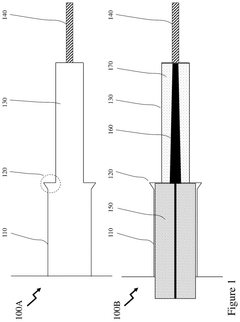
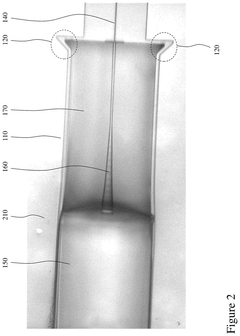
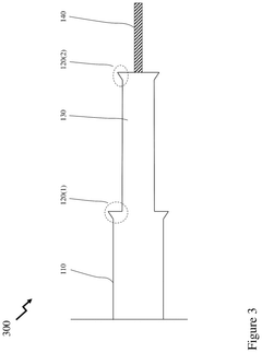
Photonic wire bonding methods and processes for the advanced packaging of photonic devices and systems
PatentPendingUS20250154053A1
Innovation
- The development of photonic wire bonds and photonic wire bonding techniques for packaging discrete integrated optical components, allowing for the formation of optical waveguides that can be directly connected or connected via special structures between optical fibers and integrated optical waveguides, thereby enabling low-cost, low-loss optical interconnections.

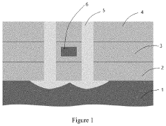
Method for packaging semiconductor structure, packaging structure, and chip
PatentInactiveUS20220308288A1
Innovation
- A method involving plasma-enhanced chemical vapor deposition (PECVD) is used to form a thin silicon oxide film that seals the trench opening without overfilling, leveraging its low step coverage to retain the cavity structure and prevent material blockage, which is then followed by subsequent packaging processes like TSV formation and copper electroplating.
Environmental Impact Assessment
Silicon photonics packaging processes involve numerous materials and manufacturing techniques that can have significant environmental implications. The environmental impact assessment of these processes reveals several critical concerns that regulators increasingly focus on. Manufacturing silicon photonic devices requires hazardous chemicals including solvents, acids, and heavy metals that pose environmental risks if improperly managed or disposed of.
Water consumption represents another major environmental concern, as silicon photonics fabrication demands substantial quantities of ultra-pure water for cleaning and processing. This consumption pattern places pressure on local water resources, particularly in regions already experiencing water scarcity. Additionally, the energy-intensive nature of clean room operations and specialized equipment contributes significantly to the carbon footprint of silicon photonics manufacturing facilities.
Waste management presents complex challenges, with semiconductor manufacturing generating various waste streams including chemical effluents, solid waste, and potentially toxic byproducts. Regulatory frameworks increasingly mandate comprehensive waste management protocols, recycling initiatives, and proper disposal methods to minimize environmental contamination.
The global supply chain for silicon photonics components introduces further environmental considerations. Raw material extraction, processing, and transportation all contribute to the overall environmental impact. Regulations increasingly require life cycle assessments that account for these upstream environmental costs, pushing manufacturers to optimize their supply chains for sustainability.
End-of-life considerations have gained regulatory attention as electronic waste continues to accumulate globally. Silicon photonic devices contain valuable and potentially harmful materials that require specialized recycling processes. Extended producer responsibility regulations increasingly hold manufacturers accountable for the entire lifecycle of their products, including proper disposal and recycling.
Climate change regulations specifically target energy-intensive industries, with carbon pricing mechanisms and emissions reporting requirements affecting silicon photonics manufacturers. Companies must now document and reduce their greenhouse gas emissions to comply with evolving climate policies. Forward-thinking organizations are implementing environmental management systems that exceed minimum compliance requirements, recognizing that proactive environmental stewardship can provide competitive advantages while reducing regulatory risks.
Risk Management Strategies
Effective risk management is essential for organizations involved in silicon photonics packaging to navigate the complex regulatory landscape while maintaining operational efficiency. A comprehensive risk management framework begins with systematic identification of compliance risks across all operational areas, including material sourcing, manufacturing processes, testing protocols, and waste management. This identification process should leverage cross-functional expertise and incorporate both historical compliance issues and emerging regulatory trends.
Risk assessment methodologies must quantify both the likelihood and potential impact of compliance failures, with particular attention to high-consequence scenarios such as product recalls, market access restrictions, or significant financial penalties. Organizations should develop a risk prioritization matrix that considers factors such as regulatory scrutiny levels, potential harm to end-users, and business continuity implications.
Mitigation strategies should follow a hierarchical approach, beginning with elimination of non-compliant materials or processes where possible, followed by engineering controls, administrative measures, and monitoring systems. Particularly effective are automated compliance verification systems that can track regulatory requirements against product specifications in real-time, flagging potential issues before they manifest in production.
Contingency planning represents another critical component, with organizations needing documented response protocols for various compliance failure scenarios. These should include clear escalation pathways, communication templates for stakeholders, and remediation procedures that address both immediate containment and root cause correction.
Regular compliance audits, both internal and third-party, provide essential verification of risk management effectiveness. These audits should evaluate not only technical compliance but also the maturity of compliance management systems and organizational compliance culture. Leading organizations implement continuous monitoring approaches rather than periodic assessments, leveraging data analytics to identify compliance drift before violations occur.
Knowledge management systems that capture compliance lessons learned and regulatory interpretations create institutional memory that enhances risk management capabilities over time. These systems should be accessible across organizational boundaries to ensure consistent application of compliance knowledge throughout the product lifecycle.
Finally, effective risk management requires appropriate governance structures with clear accountability for compliance outcomes. This typically includes dedicated compliance roles, executive-level oversight, and integration of compliance metrics into performance management systems at multiple organizational levels.
Unlock deeper insights with Patsnap Eureka Quick Research — get a full tech report to explore trends and direct your research. Try now!
Generate Your Research Report Instantly with AI Agent
Supercharge your innovation with Patsnap Eureka AI Agent Platform!