What Are the Key Standards for Silicon Photonics Packaging
SEP 29, 20259 MIN READ
Generate Your Research Report Instantly with AI Agent
Patsnap Eureka helps you evaluate technical feasibility & market potential.
Silicon Photonics Packaging Background and Objectives
Silicon photonics has emerged as a transformative technology in the semiconductor industry over the past two decades, offering unprecedented integration of optical and electronic components on a single chip. This integration promises significant advantages in data transmission speed, energy efficiency, and scalability compared to traditional electronic interconnects. The evolution of silicon photonics technology has been marked by continuous improvements in manufacturing processes, component design, and integration techniques.
The packaging of silicon photonic devices represents a critical aspect of this technology's development trajectory. Unlike conventional electronic packaging, silicon photonics packaging must address unique challenges related to optical alignment precision, thermal management, and the interface between optical and electrical domains. The historical progression of packaging solutions has evolved from simple edge-coupling approaches to more sophisticated 3D integration strategies that enable higher density and performance.
Current market trends indicate a growing demand for standardized packaging solutions that can support high-volume manufacturing while maintaining the stringent performance requirements of photonic systems. This standardization is essential for the broader adoption of silicon photonics across various application domains, including data centers, telecommunications, sensing, and emerging quantum computing platforms.
The primary objectives of silicon photonics packaging standardization include establishing common interfaces, defining reliable testing methodologies, ensuring interoperability between components from different manufacturers, and reducing overall production costs. These standards must address critical parameters such as optical coupling efficiency, alignment tolerance, thermal stability, and long-term reliability under various operating conditions.
Technical goals for silicon photonics packaging standards encompass several dimensions: achieving sub-micron alignment precision for optical coupling, developing hermetic sealing techniques compatible with optical interfaces, establishing standardized fiber attachment methods, and creating unified approaches to thermal management that can accommodate the unique requirements of photonic integrated circuits.
The evolution of these standards is being driven by collaborative efforts between industry consortia, academic institutions, and standards organizations. Key milestones in this journey include the development of reference designs, the establishment of common terminology and measurement protocols, and the creation of certification processes that ensure compliance with established standards.
As silicon photonics continues to mature as a technology platform, the development of comprehensive packaging standards will play a pivotal role in facilitating its transition from specialized applications to mainstream deployment across multiple industries and use cases.
Market Demand Analysis for Silicon Photonics Solutions
The silicon photonics market is experiencing unprecedented growth, driven by increasing demands for high-speed data transmission, cloud computing infrastructure, and telecommunications advancements. Current market analysis indicates that the global silicon photonics market is projected to reach $3.5 billion by 2025, with a compound annual growth rate exceeding 20% between 2020-2025. This remarkable growth trajectory is primarily fueled by data center applications, which currently account for approximately 60% of the market share.
The demand for silicon photonics packaging solutions is particularly acute in hyperscale data centers, where bandwidth requirements continue to escalate exponentially. Industry reports highlight that data traffic within data centers is doubling approximately every two years, creating urgent needs for higher-capacity, energy-efficient interconnect solutions that silicon photonics can provide.
Telecommunications represents the second-largest market segment, with 5G infrastructure deployment creating substantial demand for silicon photonics components. The need for high-bandwidth, low-latency connections is driving adoption across metropolitan, regional, and long-haul networks. Telecom operators are increasingly looking toward silicon photonics to address bandwidth bottlenecks while reducing power consumption.
Consumer electronics applications are emerging as a promising growth sector, particularly in high-performance computing devices and augmented reality systems. Market research indicates that silicon photonics could penetrate up to 15% of consumer electronics requiring high-bandwidth connections by 2027, representing a significant expansion from current minimal market presence.
From a geographical perspective, North America currently dominates the silicon photonics market with approximately 40% share, followed by Europe and Asia-Pacific. However, the Asia-Pacific region is expected to witness the highest growth rate over the next five years, driven by massive investments in data center infrastructure in China, Japan, and Singapore.
Customer requirements are increasingly focused on standardized packaging solutions that can enable seamless integration with existing systems while providing clear migration paths for future upgrades. Survey data from major data center operators indicates that 78% consider standardized packaging interfaces a "critical" or "very important" factor in adoption decisions.
Cost remains a significant market barrier, with current silicon photonics solutions typically commanding a 30-40% premium over conventional technologies. Market analysis suggests that achieving price parity with traditional interconnect technologies would potentially triple the addressable market within three years, highlighting the critical importance of cost-effective packaging standards and manufacturing processes.
Current Standards and Technical Challenges in Photonic Packaging
Silicon photonics packaging currently faces significant standardization challenges despite its growing importance in optical communication systems. The industry lacks comprehensive, universally accepted standards, creating obstacles for mass production and interoperability. Several organizations are working to address this gap, including the IEEE P3172 working group focused on silicon photonic integrated circuits, and the IEC's efforts through its TC86 committee on fiber optics.
The Optical Internetworking Forum (OIF) has made notable contributions with its Implementation Agreements, particularly for coherent optical interfaces. These agreements provide specifications for form factors, electrical interfaces, and thermal management, serving as de facto standards in the absence of formal ones. Similarly, the Consortium for On-Board Optics (COBO) has developed specifications for on-board optical modules that influence silicon photonics packaging approaches.
Current packaging standards primarily address mechanical dimensions, thermal specifications, electrical interfaces, and optical coupling methodologies. For mechanical aspects, standards define package outlines, mounting features, and physical interfaces. Thermal specifications establish operating temperature ranges and heat dissipation requirements. Electrical interface standards cover high-speed signal integrity, power delivery, and grounding schemes. Optical coupling standards address fiber attachment methods, alignment tolerances, and coupling efficiency requirements.
Despite these efforts, significant technical challenges persist. Alignment precision remains critical, as silicon photonic devices require sub-micron alignment accuracy between optical components and fibers, far exceeding traditional electronic packaging tolerances. This precision must be maintained across temperature variations and throughout the product lifecycle, necessitating advanced packaging solutions.
Thermal management presents another major challenge. Silicon photonic devices are temperature-sensitive, with wavelength shifts of approximately 0.1 nm/°C in resonant structures. Effective heat dissipation while maintaining optical alignment integrity requires innovative approaches not fully addressed by current standards.
Hermeticity requirements also pose difficulties. Photonic components often require protection from moisture and contaminants that can degrade optical performance. Standard electronic packaging approaches may not provide adequate protection for optical interfaces and components, necessitating specialized solutions.
Testing and qualification methodologies represent another standardization gap. Unlike electronic components with established testing protocols, silicon photonic devices require specialized optical testing procedures that are not yet standardized across the industry. This lack of standardized testing increases manufacturing costs and complicates quality assurance.
The fragmentation of standards across different organizations and application domains further complicates the landscape. Companies must navigate multiple, sometimes conflicting specifications depending on their target markets, hindering economies of scale and increasing development costs.
Mainstream Packaging Solutions and Implementation Approaches
01 Standardized Packaging Interfaces for Silicon Photonics
Standardized interfaces for silicon photonic packaging enable interoperability between different components and systems. These standards define specifications for optical and electrical connections, ensuring compatibility across various manufacturers. Standardized interfaces reduce integration complexity and facilitate the development of modular photonic systems, allowing for easier assembly and testing of silicon photonic devices.- Standardized Packaging Interfaces for Silicon Photonics: Standardized interfaces for silicon photonic packaging enable interoperability between different components and systems. These standards define specifications for optical coupling, electrical connections, and mechanical alignment to ensure compatibility across various manufacturers. Standardized interfaces reduce integration complexity and manufacturing costs while improving reliability in photonic integrated circuits.
- Thermal Management Solutions in Silicon Photonic Packaging: Thermal management is critical in silicon photonic packaging to maintain operational stability and reliability. Various approaches include integrated heat sinks, thermally conductive materials, and active cooling systems to dissipate heat generated during operation. Effective thermal management prevents wavelength drift, reduces signal degradation, and extends the operational lifetime of silicon photonic devices.
- Hermetic Sealing and Environmental Protection Standards: Hermetic sealing and environmental protection standards for silicon photonic packages ensure long-term reliability and performance stability. These standards specify materials and techniques for protecting sensitive optical components from moisture, dust, and other environmental contaminants. Proper environmental isolation prevents degradation of optical surfaces and maintains coupling efficiency between components.
- Fiber-to-Chip Coupling Standardization: Standardized approaches for fiber-to-chip coupling in silicon photonics address one of the most challenging aspects of photonic packaging. These standards define specifications for edge coupling, vertical grating couplers, and mode size converters to efficiently transfer light between optical fibers and integrated waveguides. Standardized coupling methods reduce insertion loss, improve manufacturing yield, and enable automated assembly processes.
- Electrical-Optical Integration Standards for Co-packaged Optics: Standards for electrical-optical integration in co-packaged optics define specifications for combining electronic and photonic components in a single package. These standards address signal integrity, power delivery, and high-speed interfaces between electronic ICs and photonic circuits. Standardized co-packaging approaches enable higher bandwidth density, reduced power consumption, and smaller form factors for data center and telecommunications applications.
02 Thermal Management Solutions in Silicon Photonic Packaging
Thermal management is critical in silicon photonic packaging to maintain optimal performance and reliability. Various approaches include integrated heat sinks, thermal interface materials, and active cooling systems designed specifically for photonic integrated circuits. Effective thermal solutions address the temperature sensitivity of optical components and prevent wavelength drift, ensuring consistent operation across varying environmental conditions.Expand Specific Solutions03 Fiber-to-Chip Coupling Standards
Standardized methods for coupling optical fibers to silicon photonic chips are essential for efficient light transmission. These standards define specifications for alignment tolerances, coupling efficiency, and mechanical stability. Various coupling techniques include edge coupling, grating couplers, and butt coupling, each with standardized interfaces to ensure consistent optical performance and manufacturability across different packaging platforms.Expand Specific Solutions04 Hermetic Sealing and Environmental Protection Standards
Standards for hermetic sealing and environmental protection ensure the long-term reliability of silicon photonic packages. These specifications define requirements for moisture resistance, contamination control, and mechanical protection. Standardized testing protocols verify the integrity of hermetic seals and the package's ability to withstand environmental stresses, including temperature cycling, humidity, and mechanical shock.Expand Specific Solutions05 Integration Standards for Electronic-Photonic Co-packaging
Standards for electronic-photonic co-packaging address the integration of electronic and photonic components within a single package. These specifications define electrical and optical interconnect requirements, signal integrity parameters, and power distribution architectures. Co-packaging standards enable high-bandwidth, low-latency communication between electronic processors and photonic transceivers while maintaining manufacturability and testability.Expand Specific Solutions
Major Industry Players and Standardization Bodies
Silicon photonics packaging standards are evolving within a rapidly growing market, currently in its early maturity phase with significant expansion potential. The global silicon photonics market is projected to reach $3-4 billion by 2025, driven by data center and telecommunications applications. Technical standardization remains fragmented, with key players developing proprietary and collaborative approaches. TSMC, Intel, and GlobalFoundries are advancing foundry-compatible packaging solutions, while IBM and Huawei focus on integration with existing optical networks. Academic-industry partnerships involving institutions like Huazhong University and companies such as AEPONYX are addressing thermal management and coupling efficiency challenges. The industry is moving toward standardization in optical I/O interfaces, thermal specifications, and testing methodologies to enable broader adoption.
Taiwan Semiconductor Manufacturing Co., Ltd.
Technical Solution: TSMC has established silicon photonics packaging standards through their integrated photonics platform, focusing on wafer-level packaging techniques that leverage their advanced semiconductor manufacturing capabilities. Their approach emphasizes standardized optical I/O interfaces compatible with fiber array attachment using passive alignment techniques. TSMC has developed specific design rules for photonic-electronic integration with standardized process design kits (PDKs) that ensure compatibility between their photonic and electronic components. Their packaging standards address hermeticity requirements for photonic components with specialized sealing techniques that maintain optical performance over device lifetime. TSMC has also contributed to industry standardization efforts through collaboration with the IEEE P3186 working group on silicon photonics standards, helping establish reference architectures for photonic integrated circuits. Their packaging technology supports multi-channel optical transceivers with standardized channel spacing and data rates up to 50 Gbps per channel.
Strengths: World-class manufacturing infrastructure enabling high-volume production with excellent yield and reliability. Comprehensive PDK ecosystem supporting diverse photonic designs. Weaknesses: Less vertical integration compared to some competitors, potentially requiring additional partnerships for complete solutions.
Advanced Semiconductor Engineering, Inc.
Technical Solution: ASE has established comprehensive standards for silicon photonics packaging through their Advanced Optical Packaging platform. Their approach focuses on specialized assembly techniques for photonic components, including precision die attach methods with sub-micron alignment accuracy for optical coupling. ASE has developed standardized processes for fiber array attachment using automated active alignment systems that optimize coupling efficiency between optical fibers and on-chip waveguides. Their packaging standards address thermal management challenges through specialized materials and designs that minimize thermal gradients across photonic components. ASE has established specific design rules for optical interface standardization, including pitch, alignment tolerances, and physical protection structures. They've contributed to industry standards through participation in the Photonics Components Packaging Consortium (PCPC), helping establish reference designs for optical engine packaging. Their technology supports various coupling approaches including edge coupling, grating coupling, and butt coupling with standardized specifications for each method.
Strengths: Industry-leading expertise in advanced packaging technologies with high-precision assembly capabilities. Extensive experience with heterogeneous integration of diverse materials and components. Weaknesses: More dependent on upstream design and fabrication partners compared to integrated device manufacturers.
Critical Patents and Technical Literature in Photonic Packaging
Spectral purity filter, lithographic apparatus, and method for manufacturing a spectral purity filter
PatentWO2011000622A1
Innovation
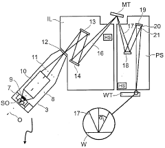
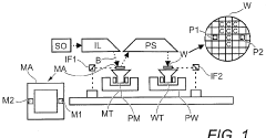
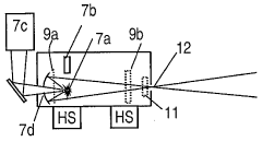
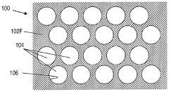
- A spectral purity filter with a grid-like structure fabricated from semiconductor material like silicon, coated with hydrogen-resistant materials such as silicon nitride, silicon dioxide, or silicon carbide, featuring apertures with textured sidewalls to enhance radiation suppression and durability.
Compositions useful as chromatography stationary phases
PatentActiveUS20080293959A1
Innovation
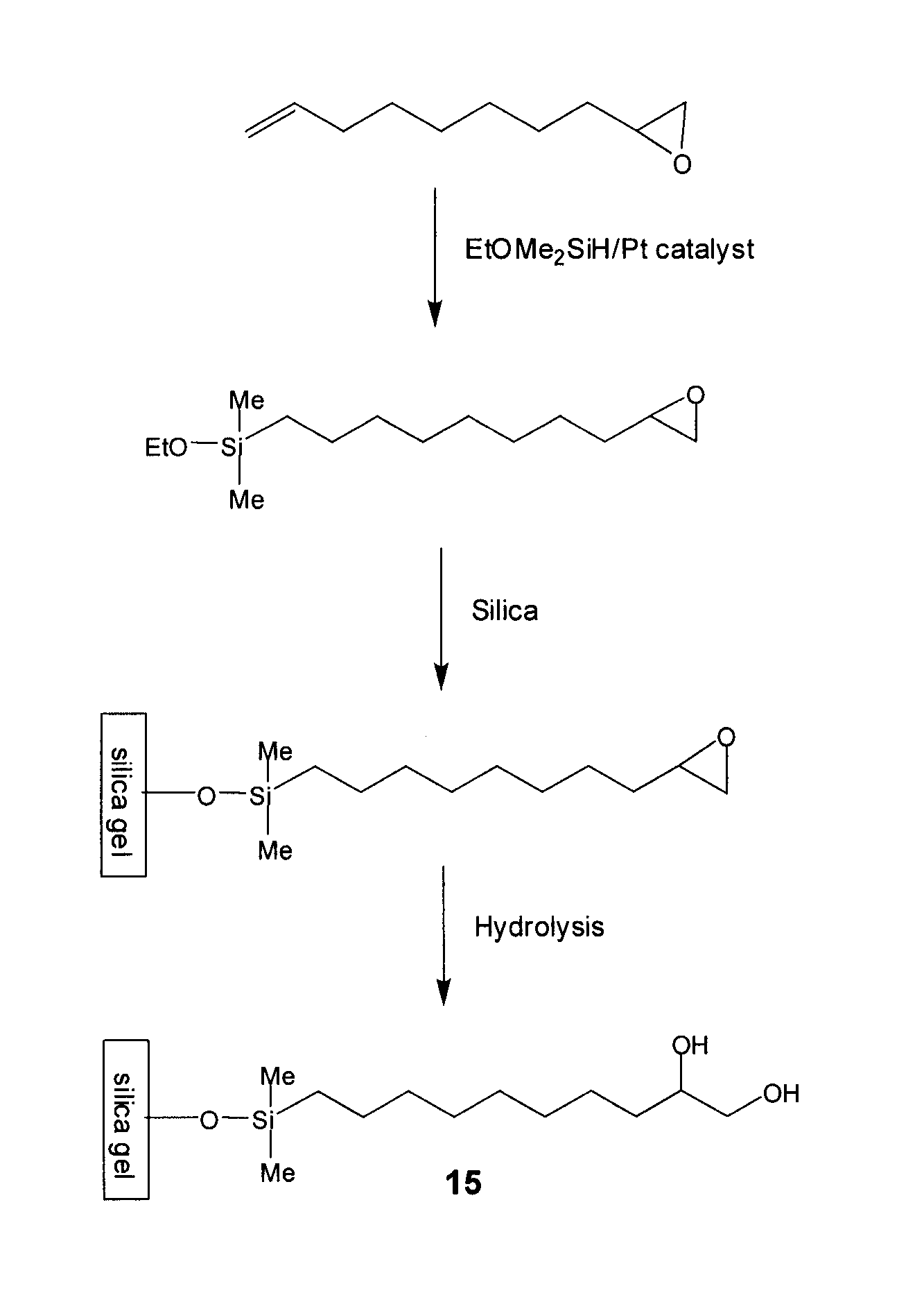
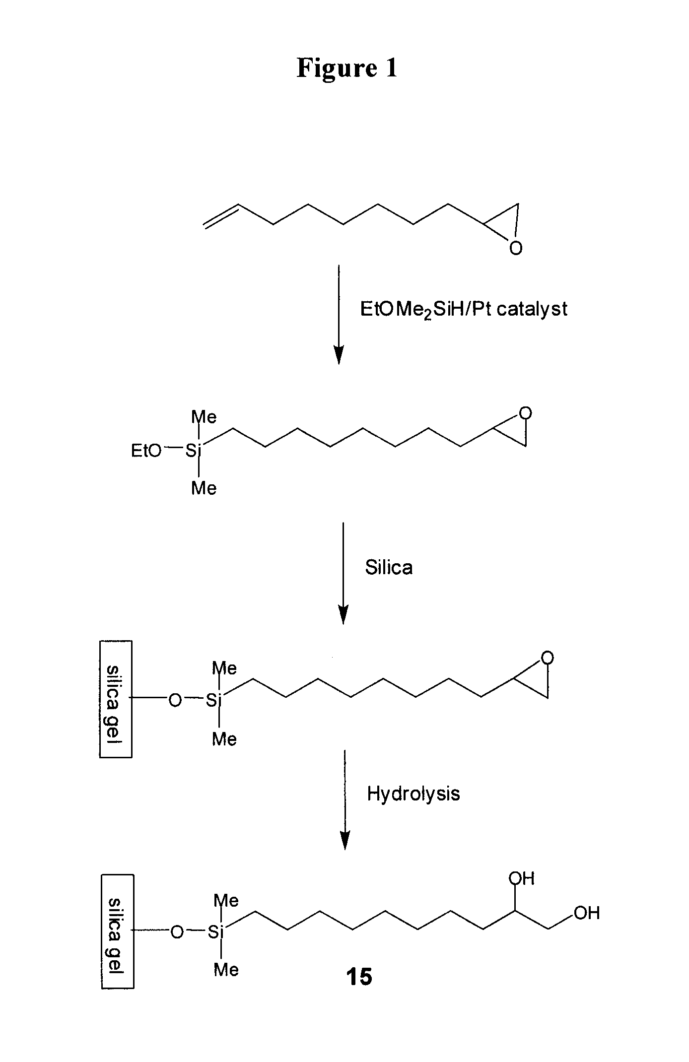
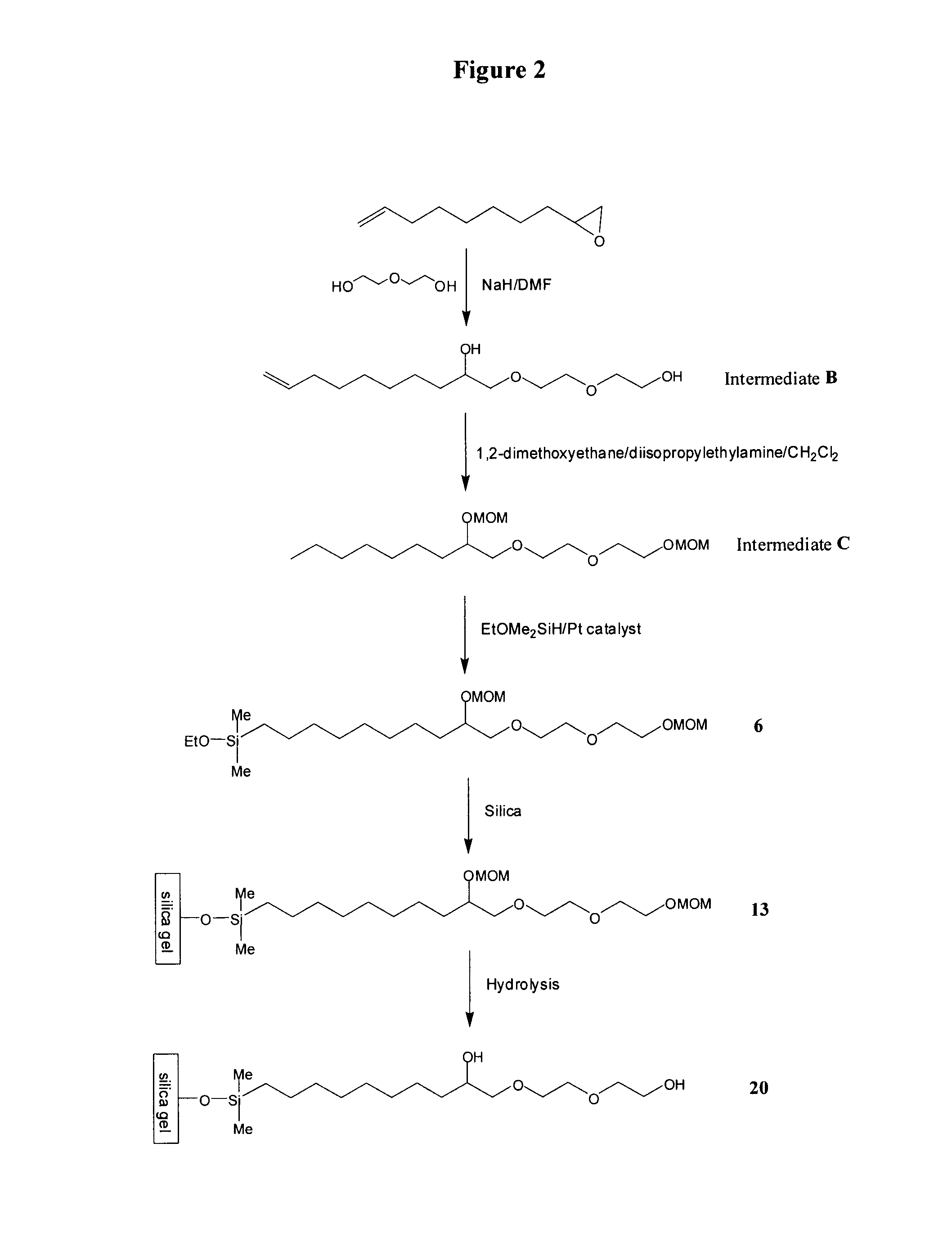
- Development of chromatographic stationary phases with both hydrophobic and hydrophilic moieties covalently bound to a substrate, allowing for use in both HILIC and RP modes, enhancing retention and selectivity for polar and non-polar molecules, and providing improved equilibration times and chemical stability.
Interoperability and Compatibility Considerations
Interoperability and compatibility represent critical considerations in silicon photonics packaging standardization, as they directly impact the integration capabilities across different platforms and technologies. The silicon photonics ecosystem encompasses multiple vendors, manufacturing processes, and design methodologies, necessitating robust standards to ensure seamless interaction between components.
Current silicon photonics packaging standards address interoperability through standardized optical interfaces, electrical connections, and thermal management specifications. Organizations such as the Optical Internetworking Forum (OIF) and IEEE have developed implementation agreements that define interface parameters, ensuring components from different manufacturers can work together effectively. These standards typically specify wavelength ranges, optical power levels, and signal integrity requirements that must be maintained across interconnection points.
Compatibility with existing optical communication infrastructure presents another crucial dimension. Standards must facilitate the integration of silicon photonics modules with conventional optical fiber networks, electronic integrated circuits, and established data center architectures. This backward compatibility ensures that investments in existing infrastructure remain protected while enabling the adoption of silicon photonics technology.
Cross-platform compatibility standards address the integration challenges between silicon photonics and electronic ICs, particularly regarding signal integrity at high data rates. Standards like IEEE 802.3 and OIF-CEI define electrical interface specifications that ensure proper signal transmission between photonic and electronic domains. These standards typically specify impedance matching requirements, signal timing parameters, and power delivery specifications.
Testing and verification protocols form an essential component of interoperability standards. Organizations like the Joint Electron Device Engineering Council (JEDEC) have developed standardized testing methodologies to verify compliance with interoperability requirements. These protocols ensure that silicon photonics packages meet performance specifications across various operating conditions and integration scenarios.
Future interoperability standards are evolving to address emerging challenges in heterogeneous integration, where silicon photonics components must interface with diverse technologies such as electronic ICs, MEMS devices, and specialized sensors. The development of these standards requires collaboration between industry consortia, academic institutions, and standards organizations to ensure broad applicability and adoption across the silicon photonics ecosystem.
Environmental Impact and Sustainability of Packaging Materials
The environmental impact of silicon photonics packaging represents a critical consideration as this technology scales toward mass production. Traditional semiconductor packaging often involves materials with significant ecological footprints, including heavy metals, halogenated flame retardants, and energy-intensive manufacturing processes. Silicon photonics packaging, while offering advantages in terms of miniaturization and performance, presents unique sustainability challenges that industry standards must address.
Current environmental standards for silicon photonics packaging primarily focus on compliance with regulations such as the Restriction of Hazardous Substances (RoHS) and Waste Electrical and Electronic Equipment (WEEE) directives. These frameworks limit the use of lead, mercury, cadmium, and other harmful substances in electronic components. However, the specialized nature of photonic packaging—requiring precise optical alignment and hermetic sealing—often necessitates materials and processes not fully optimized for environmental sustainability.
The carbon footprint of silicon photonics packaging stems largely from energy-intensive manufacturing processes, particularly those requiring high-temperature processing and ultra-clean environments. Standards addressing energy efficiency in manufacturing, such as ISO 50001, are increasingly being applied to photonics fabrication facilities. Additionally, the International Electrotechnical Commission (IEC) has begun developing specific guidelines for energy consumption assessment in photonic component production.
Material selection represents another critical environmental consideration. Gold, commonly used for wire bonding in photonic packages, has significant environmental impacts associated with its mining and processing. Industry standards are evolving to promote alternatives such as copper interconnects where technically feasible. Similarly, standards addressing the use of rare earth elements in optical components aim to reduce dependence on materials with problematic supply chains and extraction impacts.
End-of-life management presents particular challenges for photonic packages due to their hybrid nature—combining electronic, optical, and sometimes fluidic elements. The IEEE 1680 family of standards for environmental assessment of electronic products is being adapted to address the unique recycling challenges of integrated photonic devices. These standards promote design for disassembly and material recovery, crucial for reducing electronic waste.
Water usage in silicon photonics manufacturing is substantial, with cleaning and cooling processes consuming significant volumes. Emerging standards from organizations like SEMI are establishing benchmarks for water recycling and conservation in semiconductor and photonics facilities. These standards recognize the growing water scarcity concerns in many regions where high-tech manufacturing occurs.
Unlock deeper insights with Patsnap Eureka Quick Research — get a full tech report to explore trends and direct your research. Try now!
Generate Your Research Report Instantly with AI Agent
Supercharge your innovation with Patsnap Eureka AI Agent Platform!
