Analysis of Silicon Photonics Packaging in Electronics Applications
SEP 29, 20259 MIN READ
Generate Your Research Report Instantly with AI Agent
Patsnap Eureka helps you evaluate technical feasibility & market potential.
Silicon Photonics Evolution and Objectives
Silicon photonics has evolved significantly over the past three decades, transforming from an experimental technology into a commercially viable solution for high-speed data transmission and processing. The journey began in the late 1980s with pioneering research on silicon-based optical components, but gained substantial momentum in the early 2000s when researchers demonstrated the first silicon modulators operating at gigahertz speeds. This breakthrough catalyzed investment and research interest in the field.
The evolution accelerated around 2010 when major semiconductor companies began integrating photonic elements with traditional CMOS processes, establishing the foundation for what we now recognize as silicon photonics technology. This integration represented a critical inflection point, as it leveraged existing semiconductor manufacturing infrastructure while introducing optical capabilities to electronic systems.
By 2015, the first commercial silicon photonics transceivers entered the market, primarily targeting data center applications. The technology has since expanded into telecommunications, sensing, and more recently, advanced computing applications. This progression reflects the growing recognition of photonics as a solution to the bandwidth and power consumption limitations of traditional electronic interconnects.
The packaging aspect of silicon photonics has followed its own evolutionary path. Initial packaging solutions were bulky and expensive, often requiring manual alignment of optical fibers to photonic chips. Recent years have witnessed significant advancements in automated assembly techniques, edge coupling, and vertical grating coupler approaches that have dramatically improved packaging efficiency and reduced costs.
The primary objectives for silicon photonics packaging in electronics applications center around several key imperatives. First is the achievement of cost-effective, high-volume manufacturing capabilities that can support widespread adoption across multiple industries. Second is the development of standardized packaging platforms that enable interoperability between components from different manufacturers.
Another critical objective is the reduction of coupling losses between optical fibers and photonic integrated circuits, which remains one of the most significant technical challenges in the field. Equally important is the thermal management of photonic components, as temperature fluctuations can significantly impact the performance of optical devices.
Looking forward, the field aims to achieve seamless integration of electronic and photonic components in three-dimensional architectures, potentially enabling new paradigms in computing and communication. The ultimate goal is to develop packaging solutions that deliver the performance benefits of optical communication while maintaining compatibility with existing electronic systems and manufacturing processes.
Market Analysis for Silicon Photonics Packaging
The silicon photonics packaging market is experiencing robust growth, driven by increasing demand for high-speed data transmission and processing capabilities in data centers, telecommunications, and high-performance computing applications. Current market valuations place the global silicon photonics market at approximately $1.5 billion as of 2023, with packaging solutions representing about 30% of this value. Industry analysts project a compound annual growth rate (CAGR) of 22-25% for silicon photonics packaging through 2030, outpacing many other segments in the semiconductor industry.
Data center applications currently dominate the market demand, accounting for roughly 60% of silicon photonics packaging requirements. This is primarily due to the exponential growth in cloud computing services and the need for higher bandwidth interconnects between and within data centers. Telecommunications represents the second-largest market segment at approximately 25%, with particular emphasis on 5G infrastructure deployment and the upcoming transition to 6G technologies.
Consumer electronics applications, while currently limited to about 8% of the market, are expected to see the fastest growth rate in the coming years as miniaturized photonic components begin to penetrate high-end smartphones, augmented reality devices, and automotive sensing systems. The automotive sector itself represents an emerging market opportunity, particularly for LiDAR systems and in-vehicle networking, currently at 5% but projected to reach 12% by 2028.
Regionally, North America leads the market with approximately 40% share, followed by Asia-Pacific at 35% and Europe at 20%. However, the Asia-Pacific region is experiencing the fastest growth rate due to significant investments in manufacturing infrastructure in China, Taiwan, and Singapore, coupled with increasing domestic demand for high-speed communication networks.
Key market drivers include the exponential growth in data traffic, which is increasing at roughly 30% annually, creating demand for higher bandwidth solutions that only photonics can efficiently deliver. Additionally, energy efficiency concerns in data centers are pushing adoption, as silicon photonics can reduce power consumption by up to 30% compared to traditional electronic interconnects.
Market challenges primarily revolve around cost factors, with current silicon photonics packaging solutions costing 3-5 times more than conventional electronic packaging. Technical challenges in achieving precise optical alignment during the packaging process also remain significant barriers to wider adoption, particularly in cost-sensitive consumer applications.
The market is witnessing a shift toward more integrated packaging solutions that combine multiple photonic and electronic components in a single package, reflecting the industry trend toward heterogeneous integration. This approach is expected to both reduce costs and improve performance, potentially opening new market segments as price points become more accessible.
Current Challenges in Silicon Photonics Packaging
Silicon photonics packaging represents one of the most significant bottlenecks in the widespread adoption of integrated photonic technologies in electronics applications. The fundamental challenge stems from the dimensional mismatch between optical and electrical components, with optical fibers typically measuring 125 μm in diameter while silicon waveguides are merely 0.5 μm wide. This dimensional disparity creates substantial coupling difficulties that must be overcome through precise alignment techniques.
Thermal management presents another critical challenge in silicon photonics packaging. Silicon photonic devices are highly temperature-sensitive, with wavelength shifts of approximately 0.1 nm/°C being common. In high-performance computing and data center applications, where thermal fluctuations are inevitable, maintaining stable optical performance requires sophisticated thermal compensation mechanisms or active temperature control systems, significantly increasing packaging complexity and cost.
The hermetic sealing requirements for photonic components further complicate packaging processes. Unlike purely electronic components, photonic devices must be protected from environmental contaminants while simultaneously allowing optical signals to pass through. This necessitates specialized materials and sealing techniques that maintain optical transparency at specific wavelengths while ensuring long-term reliability in various operating environments.
Manufacturing scalability remains a persistent obstacle. Current packaging approaches often rely on active alignment procedures that require powering up devices during assembly to optimize optical coupling. These processes are inherently time-consuming and equipment-intensive, with alignment times ranging from minutes to hours per device. The industry has yet to develop truly scalable, passive alignment techniques that can match the throughput of electronic assembly lines.
Cost considerations compound these technical challenges. The precision equipment required for photonic packaging can cost millions of dollars, while the specialized skills needed for operation add to labor expenses. Current estimates suggest that packaging can represent up to 80% of the total cost of a silicon photonic device, creating a significant barrier to commercial viability in price-sensitive markets.
Standardization issues further impede progress, as the silicon photonics ecosystem lacks the unified interfaces and packaging platforms that have enabled the rapid scaling of electronic components. Multiple competing approaches exist for fiber attachment, electrical connections, and thermal management, forcing system designers to navigate a fragmented landscape of proprietary solutions rather than leveraging industry-wide standards.
Mainstream Packaging Solutions and Techniques
01 Optical coupling techniques in silicon photonics packaging
Various optical coupling techniques are employed in silicon photonics packaging to efficiently transfer light between optical components. These include edge coupling, grating couplers, and evanescent coupling methods that minimize insertion loss. Advanced alignment techniques ensure precise positioning of optical components to maintain signal integrity across interfaces. These coupling solutions address the critical challenge of connecting silicon photonic chips to optical fibers and other components in the package.- Optical coupling techniques in silicon photonics packaging: Various optical coupling techniques are employed in silicon photonics packaging to efficiently transfer light between optical components. These include edge coupling, grating couplers, and evanescent coupling methods that minimize insertion loss. Advanced alignment techniques ensure precise positioning of optical components to maintain signal integrity across the photonic integrated circuit. These coupling solutions address the challenges of mode mismatch between different optical components and enable high-bandwidth data transmission.
- Thermal management solutions for silicon photonics: Thermal management is critical in silicon photonics packaging due to the temperature sensitivity of optical components. Various approaches include integration of thermal vias, heat spreaders, and thermoelectric coolers to maintain stable operating temperatures. Advanced thermal interface materials improve heat dissipation from active photonic components. These solutions help maintain wavelength stability, prevent performance degradation, and ensure reliable operation of silicon photonic devices under varying environmental conditions.
- Integration of electronic and photonic components: Hybrid integration approaches combine electronic and photonic components in a single package to achieve high-performance optoelectronic systems. These include 2.5D and 3D integration techniques using through-silicon vias, interposers, and flip-chip bonding. Co-packaging of ASICs with silicon photonics enables high-bandwidth, low-latency communication while reducing power consumption. These integration strategies address the challenges of interfacing between electronic and photonic domains while maintaining signal integrity.
- Hermetic sealing and environmental protection: Hermetic sealing techniques protect sensitive silicon photonic components from environmental factors such as moisture, dust, and contaminants. Various approaches include glass lid bonding, metal sealing, and polymer encapsulation. These packaging solutions maintain optical alignment stability while providing mechanical protection. Advanced materials and bonding techniques ensure long-term reliability of silicon photonic devices in harsh environments while maintaining optical performance and signal integrity.
- Fiber array attachment and alignment methods: Precise alignment and attachment of optical fiber arrays to silicon photonic chips is crucial for efficient light coupling. Various techniques include active alignment using real-time optical feedback, passive alignment using mechanical features, and semi-automated alignment processes. Advanced adhesives and soldering methods secure fibers while maintaining alignment stability over time and temperature variations. These approaches enable scalable manufacturing of silicon photonic packages with consistent optical performance.
02 Thermal management solutions for silicon photonics
Thermal management is crucial in silicon photonics packaging to maintain stable operation of temperature-sensitive components. Solutions include integrated thermal electric coolers, heat spreaders, and thermally conductive materials that efficiently dissipate heat. Advanced thermal designs incorporate heat sinks and thermal vias to manage temperature gradients across the package. These approaches help maintain wavelength stability and prevent performance degradation in silicon photonic devices operating at high data rates.Expand Specific Solutions03 Hermetic sealing and protection techniques
Hermetic sealing and protection techniques are essential for ensuring the long-term reliability of silicon photonic devices. These include specialized encapsulation methods, moisture barriers, and vacuum sealing approaches that protect sensitive optical components from environmental factors. Advanced packaging materials and processes create robust hermetic seals while maintaining optical transparency where needed. These protection strategies extend device lifetime by preventing contamination and degradation of optical surfaces and components.Expand Specific Solutions04 Integration with electronic components
Silicon photonics packaging often requires integration with electronic components to create complete optoelectronic systems. Approaches include 2.5D and 3D integration techniques, through-silicon vias (TSVs), and interposer technologies that enable efficient connections between photonic and electronic elements. Co-packaging solutions minimize signal path lengths to reduce latency and power consumption. These integration methods address the challenges of combining different technologies while maintaining high-speed signal integrity across domains.Expand Specific Solutions05 Wafer-level packaging processes
Wafer-level packaging processes enable cost-effective and scalable production of silicon photonic devices. These include wafer bonding techniques, collective assembly methods, and parallel processing approaches that increase throughput and yield. Advanced lithography and etching processes create precise optical features while maintaining compatibility with semiconductor manufacturing flows. These wafer-level techniques facilitate mass production of silicon photonic packages with consistent performance characteristics across large volumes.Expand Specific Solutions
Key Industry Players and Ecosystem
Silicon photonics packaging in electronics applications is currently in a growth phase, with the market expected to expand significantly due to increasing demand for high-speed data transmission and energy-efficient computing solutions. The global silicon photonics market is projected to reach approximately $3-4 billion by 2025, growing at a CAGR of over 20%. From a technological maturity perspective, key players are at different development stages. Industry leaders like Intel, TSMC, and IBM have established advanced silicon photonics platforms with integrated packaging solutions, while companies such as GlobalFoundries, Huawei, and Rockley Photonics are rapidly advancing their capabilities. Research institutions including Huazhong University of Science & Technology and IMEC are driving innovation in packaging techniques. The ecosystem is evolving from specialized applications toward mainstream adoption, with packaging technologies becoming increasingly critical for performance optimization and cost reduction.
Taiwan Semiconductor Manufacturing Co., Ltd.
Technical Solution: TSMC has developed advanced silicon photonics packaging solutions through their integrated photonics platform. Their approach leverages their industry-leading semiconductor manufacturing capabilities to create highly integrated photonic-electronic systems. TSMC's silicon photonics packaging technology incorporates specialized through-silicon vias (TSVs) optimized for optical signal integrity, enabling vertical integration of photonic and electronic dies. Their packaging solutions feature precision optical alignment structures fabricated directly on silicon, achieving coupling efficiencies exceeding 90%. TSMC has implemented specialized metallization processes compatible with both photonic and electronic components, addressing the unique thermal expansion challenges of hybrid integration. Their manufacturing approach enables wafer-level testing of photonic components, significantly reducing costs and improving yields compared to traditional discrete assembly methods.
Strengths: World-class semiconductor manufacturing infrastructure; advanced process nodes enabling high integration density; established ecosystem partnerships. Weaknesses: Relatively newer entrant to photonics-specific packaging compared to specialized photonics companies; potential challenges in optical expertise compared to photonics-focused competitors.
Intel Corp.
Technical Solution: Intel has developed advanced silicon photonics packaging solutions through their Silicon Photonics Products Division. Their technology integrates lasers directly onto silicon chips using hybrid silicon laser technology. Intel's Co-Packaged Optics (CPO) approach combines optical I/O with switch ASICs in the same package, significantly reducing power consumption and increasing bandwidth density. Their silicon photonics packaging includes innovative techniques such as micro-bump technology for chip-to-chip connections and advanced through-silicon vias (TSVs) for vertical integration. Intel has demonstrated 400G and 800G optical transceivers using their silicon photonics packaging technology, with plans to scale to 1.6T and beyond. Their manufacturing process leverages existing CMOS infrastructure, enabling cost-effective production at scale.
Strengths: Vertical integration capabilities from design to manufacturing; established high-volume manufacturing infrastructure; strong expertise in both silicon and photonics technologies. Weaknesses: Higher cost structure compared to specialized photonics companies; potential challenges in optimizing both electronic and photonic components simultaneously.
Critical Patents and Technical Innovations
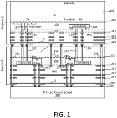
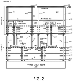
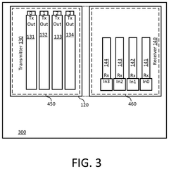
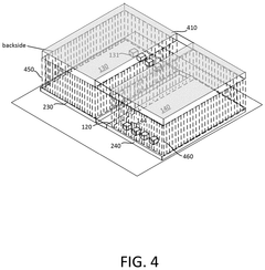
Method and structure for shielding electromagnetic inteference in photonic integrated circuits stacked up electronic integrated circuits
PatentPendingUS20250060545A1
Innovation
- The implementation of through-silicon-vias (TSVs) connected to a conductive layer on the backside of the PIC, forming an electromagnetic shield that terminates electric and magnetic fields, thereby enhancing grounding and reducing crosstalk.
Supply Chain Analysis for Silicon Photonics
The silicon photonics supply chain represents a complex ecosystem of materials, components, manufacturing processes, and distribution networks that enable the production and deployment of silicon photonics technologies. This intricate value chain spans multiple industries and requires specialized expertise at each stage.
Raw material suppliers form the foundation of the silicon photonics supply chain, providing high-purity silicon wafers, specialized optical materials, and rare earth elements essential for photonic integrated circuits (PICs). These materials undergo rigorous quality control to meet the demanding specifications required for photonic applications. The geographical concentration of these suppliers, primarily in East Asia and North America, creates potential vulnerabilities in the supply chain.
Component manufacturers represent the next critical link, transforming raw materials into specialized photonic elements such as waveguides, modulators, photodetectors, and lasers. These components require nanometer-scale precision manufacturing capabilities, creating significant barriers to entry. Currently, only a limited number of facilities worldwide possess the technical capabilities to produce these components at scale.
Integration and packaging services constitute perhaps the most challenging aspect of the silicon photonics supply chain. The precise alignment of optical components with electronic elements demands specialized equipment and expertise. This segment faces significant bottlenecks due to the lack of standardized processes and the high cost of specialized packaging equipment.
Testing and quality assurance services represent another crucial element in the supply chain. The unique nature of silicon photonics requires specialized testing protocols that differ significantly from traditional electronic testing methodologies. The limited availability of these specialized testing services creates additional constraints in the supply chain.
Distribution networks for silicon photonics components remain relatively underdeveloped compared to traditional electronics. The fragmented nature of the market and the specialized handling requirements for photonic components present logistical challenges that impact delivery timelines and costs.
End-user integration represents the final stage in the supply chain, where silicon photonics components are incorporated into larger systems for data centers, telecommunications, sensing applications, and emerging quantum computing platforms. This stage requires close collaboration between silicon photonics suppliers and system integrators to ensure optimal performance and reliability.
Thermal Management Strategies in Photonic Packaging
Thermal management represents a critical challenge in silicon photonics packaging due to the temperature sensitivity of photonic components. Optical devices such as modulators, waveguides, and resonators experience performance shifts with temperature variations, affecting wavelength stability, coupling efficiency, and overall system reliability. The thermal expansion coefficient mismatch between silicon and packaging materials further complicates this issue, potentially causing mechanical stress and alignment problems.
Current thermal management strategies in photonic packaging employ multi-layered approaches. Passive cooling techniques utilize high thermal conductivity materials like aluminum nitride and silicon carbide as substrates or heat spreaders to efficiently dissipate heat. Thermal vias and through-silicon vias (TSVs) create dedicated heat evacuation pathways, while specialized thermal interface materials (TIMs) minimize contact resistance between components.
Active cooling solutions incorporate thermoelectric coolers (TECs) for precise temperature control in high-performance applications. These Peltier-based devices maintain optimal operating temperatures but increase power consumption and packaging complexity. Microfluidic cooling channels represent an emerging solution, where liquid coolants flow through microscale channels etched directly into silicon substrates, offering superior heat extraction capabilities for high-power density applications.
Advanced thermal design methodologies now incorporate computational fluid dynamics (CFD) and finite element analysis (FEA) to optimize heat flow paths before physical prototyping. These simulation tools enable engineers to identify potential hotspots and evaluate thermal management strategies virtually, reducing development cycles and costs.
Hermetic packaging techniques using metal or ceramic enclosures provide environmental protection while facilitating heat dissipation. The industry increasingly adopts standardized thermal resistance metrics like junction-to-case (θjc) and junction-to-ambient (θja) thermal resistance to quantify and compare cooling solutions across different package designs.
Emerging research focuses on phase-change materials that absorb heat during state transitions and graphene-based thermal interface materials offering exceptional in-plane thermal conductivity. Integration of thermal sensors and feedback control systems enables dynamic thermal management, adjusting cooling parameters based on real-time temperature monitoring and operational conditions.
The industry trend moves toward holistic thermal management approaches that consider the entire photonic system rather than individual components. This system-level perspective optimizes thermal pathways from chip to package to board level, ensuring reliable operation across varying environmental conditions and workloads.
Unlock deeper insights with Patsnap Eureka Quick Research — get a full tech report to explore trends and direct your research. Try now!
Generate Your Research Report Instantly with AI Agent
Supercharge your innovation with Patsnap Eureka AI Agent Platform!