

Silicon Photonics Packaging in Consumer Electronics: A Study
SEP 29, 202510 MIN READ
Generate Your Research Report Instantly with AI Agent
PatSnap Eureka helps you evaluate technical feasibility & market potential.
Silicon Photonics Evolution and Objectives
Silicon photonics has evolved significantly over the past three decades, transforming from an experimental technology into a commercially viable solution for high-speed data transmission. The journey began in the 1980s with fundamental research on silicon as an optical material, despite initial skepticism due to silicon's indirect bandgap limiting its light emission capabilities. The 1990s marked crucial breakthroughs with the development of silicon waveguides and modulators, establishing the foundation for integrated photonic circuits.
The early 2000s witnessed accelerated progress with the first commercial silicon photonics products emerging, primarily targeting telecommunications and data center applications. During this period, researchers successfully demonstrated key components including high-speed modulators, photodetectors, and multiplexing systems on silicon platforms. The integration density and performance metrics improved exponentially, following a trajectory reminiscent of Moore's Law in traditional electronics.
By the 2010s, silicon photonics began transitioning from specialized applications to broader market segments, with major semiconductor companies investing heavily in the technology. The miniaturization of components and advances in packaging techniques enabled the first considerations for consumer electronics applications, though significant challenges remained in cost-effective manufacturing and thermal management.
The current technological landscape shows silicon photonics at an inflection point, poised to enter consumer electronics markets beyond its established presence in data centers. Recent developments in heterogeneous integration, allowing the combination of silicon with III-V materials, have addressed many of the inherent limitations of silicon as a photonic material. This hybrid approach enables efficient light sources and amplifiers while maintaining the manufacturing advantages of silicon platforms.
The primary objective of silicon photonics packaging for consumer electronics is to develop cost-effective, reliable, and miniaturized photonic integrated circuits that can be mass-produced using existing semiconductor manufacturing infrastructure. This includes achieving sub-micron alignment precision between optical components while maintaining compatibility with standard electronic packaging processes.
Additional technical objectives include reducing power consumption to levels suitable for battery-powered devices, ensuring thermal stability across varying operating conditions, and developing standardized interfaces between photonic and electronic components. The ultimate goal is to enable optical interconnects that can replace traditional copper connections in consumer devices, offering orders of magnitude improvements in bandwidth while reducing energy consumption.
Looking forward, the technology roadmap aims to achieve fully integrated silicon photonic systems-on-chip that combine sensing, computing, and communication functions in compact form factors suitable for next-generation wearables, smartphones, and augmented reality devices.
Consumer Electronics Market Demand Analysis
The consumer electronics market has witnessed a significant shift towards devices that offer higher performance, greater functionality, and smaller form factors. Silicon photonics packaging represents a transformative technology that addresses these evolving consumer demands by enabling faster data transmission, reduced power consumption, and enhanced device capabilities. Market research indicates that global consumer electronics sales reached $1.5 trillion in 2022, with smart devices incorporating advanced connectivity features showing the strongest growth trajectory.
Consumer demand for high-bandwidth applications continues to accelerate, driven by streaming services, cloud gaming, virtual reality, and augmented reality experiences. These applications require data transfer rates exceeding 100 Gbps, which traditional electronic interconnects struggle to deliver efficiently. Silicon photonics offers a compelling solution by enabling optical communication within and between devices, potentially increasing data rates by an order of magnitude while reducing energy consumption.
Smartphone manufacturers represent a key market segment expressing interest in silicon photonics technology. With annual global shipments exceeding 1.3 billion units, even incremental adoption of silicon photonics in premium models could create substantial market demand. Industry surveys indicate that 78% of smartphone users consider data transfer speed and battery life among their top five purchase considerations, directly aligning with the benefits silicon photonics can deliver.
Wearable technology presents another promising application area, with the market growing at 15% annually. As these devices become more sophisticated, incorporating health monitoring, spatial computing, and always-on connectivity features, the limitations of current interconnect technologies become increasingly apparent. Silicon photonics packaging could enable the next generation of wearables by dramatically reducing power consumption while increasing processing capabilities.
The smart home ecosystem, valued at $113 billion in 2022, represents a third significant market opportunity. As homes incorporate more connected devices—averaging 25 per household in technologically advanced markets—the need for high-bandwidth, low-latency communication becomes critical. Silicon photonics could enable seamless integration of multiple devices while addressing consumer concerns about energy efficiency.
Market analysis reveals regional variations in demand patterns. North American and European consumers prioritize performance and feature sets, while Asian markets show greater sensitivity to price-performance ratios. This suggests a phased market entry strategy may be optimal, with initial silicon photonics implementations targeting premium devices in developed markets before expanding to broader price segments.
Consumer electronics manufacturers face increasing pressure to differentiate their products in a competitive landscape. Silicon photonics packaging offers a compelling technological advantage that could drive the next wave of innovation in portable devices, potentially creating new product categories and use cases that are currently constrained by existing interconnect technologies.
Silicon Photonics Packaging Challenges
Silicon photonics packaging presents significant challenges that must be addressed for successful integration into consumer electronics. The primary obstacle lies in achieving precise optical alignment between photonic integrated circuits (PICs) and optical fibers or other components. This alignment must be maintained within sub-micron tolerances to ensure optimal light coupling efficiency, which directly impacts device performance and power consumption. The challenge is magnified in consumer electronics where environmental factors such as temperature fluctuations, vibration, and mechanical stress can disrupt this delicate alignment.
Thermal management represents another critical challenge. Silicon photonics devices generate heat during operation, which can alter refractive indices and cause wavelength shifts in optical signals. In the confined spaces of consumer electronics, effective heat dissipation becomes particularly problematic. Without proper thermal solutions, performance degradation and reliability issues emerge, limiting the practical application of silicon photonics technology in everyday devices.
Hermetic sealing requirements further complicate packaging efforts. Optical components are highly sensitive to environmental contaminants such as dust, moisture, and chemical vapors that can degrade performance over time. Creating reliable, long-lasting hermetic seals while maintaining optical pathways presents significant engineering challenges, especially when balancing against cost constraints in consumer markets.
The miniaturization demands of consumer electronics impose severe size limitations on silicon photonics packages. While traditional photonics packaging can be relatively bulky, consumer applications require ultra-compact solutions without compromising performance. This necessitates novel approaches to component integration and innovative packaging architectures that can accommodate both optical and electronic elements in extremely limited spaces.
Cost considerations represent perhaps the most formidable barrier to widespread adoption. Current silicon photonics packaging techniques often involve specialized equipment and labor-intensive processes that significantly increase manufacturing expenses. For consumer electronics, where price sensitivity is paramount, these costs must be dramatically reduced through automation, standardization, and economies of scale to achieve commercial viability.
Testing and quality assurance present unique challenges due to the hybrid nature of optoelectronic systems. Conventional electronic testing methodologies are insufficient for evaluating optical performance parameters. Developing efficient, reliable testing protocols that can be implemented in high-volume manufacturing environments remains an ongoing challenge for the industry.
Compatibility with existing electronic assembly processes constitutes another significant hurdle. To achieve mainstream adoption, silicon photonics packaging must integrate seamlessly with standard surface-mount technology (SMT) and other established manufacturing techniques used in consumer electronics production lines.
Current Packaging Solutions and Techniques
01 Optical coupling techniques in silicon photonics packaging
Various optical coupling techniques are employed in silicon photonics packaging to efficiently transfer light between optical components. These include edge coupling, grating couplers, and evanescent coupling methods that minimize insertion loss. Advanced alignment and fixation technologies ensure precise positioning of optical fibers relative to photonic integrated circuits, which is critical for maintaining high coupling efficiency in the packaged devices.- Optical coupling techniques in silicon photonics packaging: Various optical coupling techniques are employed in silicon photonics packaging to efficiently transfer light between optical components. These include edge coupling, grating couplers, and evanescent coupling methods that minimize insertion loss. Advanced alignment techniques ensure precise positioning of optical fibers relative to photonic integrated circuits, which is critical for maintaining signal integrity across the optical interface.
- Thermal management solutions for silicon photonics packages: Thermal management is crucial in silicon photonics packaging due to the temperature sensitivity of optical components. Solutions include integrated heat sinks, thermoelectric coolers, and thermally conductive materials that efficiently dissipate heat. These approaches help maintain stable operating temperatures, prevent wavelength drift, and ensure consistent performance of photonic integrated circuits under varying environmental conditions.
- Hermetic sealing and environmental protection methods: Silicon photonic devices require protection from environmental factors such as moisture, dust, and mechanical stress. Hermetic sealing techniques using glass lids, metal caps, or polymer encapsulation provide this protection while maintaining optical transparency where needed. Advanced materials and bonding methods ensure long-term reliability while accommodating the need for optical and electrical interfaces to pass through the package.
- Integration of electronic and photonic components: Hybrid integration of electronic and photonic components presents unique packaging challenges. Solutions include 2.5D and 3D integration approaches, interposer technologies, and flip-chip bonding that enable close proximity between electronic drivers and photonic circuits. These integration methods minimize signal path lengths, reduce parasitic effects, and enable compact form factors for high-performance photonic systems.
- Wafer-level packaging techniques for silicon photonics: Wafer-level packaging techniques enable cost-effective mass production of silicon photonic devices. These approaches include wafer bonding, through-silicon vias (TSVs), and collective assembly processes that allow multiple devices to be packaged simultaneously. Advanced alignment methods at the wafer level ensure optical pathways remain precisely positioned throughout the packaging process, while standardized interfaces facilitate integration into larger systems.
02 Thermal management solutions for silicon photonic packages
Thermal management is crucial in silicon photonics packaging to maintain stable operation of temperature-sensitive photonic components. Solutions include integrated thermoelectric coolers, heat spreaders, and thermally conductive materials that efficiently dissipate heat. These approaches help control the operating temperature of photonic devices, preventing wavelength drift and ensuring consistent performance across varying environmental conditions.Expand Specific Solutions03 Hermetic sealing and environmental protection methods
Hermetic sealing techniques protect sensitive silicon photonic components from environmental factors such as moisture, dust, and contaminants. Methods include glass lid bonding, metal sealing, and polymer encapsulation that maintain an inert atmosphere around the photonic circuits. These protection strategies are essential for ensuring long-term reliability and stability of silicon photonic devices in various deployment environments.Expand Specific Solutions04 Integration of electronic and photonic components
Advanced packaging approaches enable the integration of electronic and photonic components in a single package, facilitating high-bandwidth communication between them. Techniques include 2.5D and 3D integration, interposer technology, and through-silicon vias (TSVs) that create compact, high-performance optoelectronic systems. This integration is crucial for applications requiring both signal processing and optical communication capabilities.Expand Specific Solutions05 Wafer-level packaging for silicon photonics
Wafer-level packaging techniques enable mass production of silicon photonic devices with reduced costs and improved yield. These methods include wafer bonding, collective alignment, and simultaneous testing of multiple devices before singulation. The approach allows for standardized manufacturing processes that can be scaled for high-volume production while maintaining consistent quality and performance across devices.Expand Specific Solutions
Key Industry Players and Ecosystem
Silicon photonics packaging in consumer electronics is currently in a transitional phase, moving from early adoption to mainstream implementation. The market is experiencing rapid growth, projected to reach $3-4 billion by 2027, driven by increasing demand for high-speed data transmission and energy-efficient solutions. Leading players like Intel, IBM, and GlobalFoundries have established strong positions with mature manufacturing capabilities, while innovative startups such as Ayar Labs, Lightmatter, and Rockley Photonics are disrupting the space with novel integration approaches. TSMC and ASE Group provide critical manufacturing support. The technology is approaching maturity for data center applications but remains in development for consumer devices, with companies like Aeponyx and Xscape Photonics advancing miniaturization techniques essential for widespread consumer adoption.
Ayar Labs, Inc.
Technical Solution: Ayar Labs has pioneered an advanced in-package optical I/O technology called TeraPHY that specifically addresses silicon photonics packaging challenges in consumer electronics. Their solution integrates optical transceivers directly with electronic chips using advanced packaging techniques that maintain optical alignment precision while being compatible with standard assembly processes. The company's SuperNova light source works in conjunction with their TeraPHY optical I/O chiplets to deliver up to 2 Tbps of bandwidth per chiplet with energy efficiency of approximately 1 pJ/bit, representing a 10x improvement over traditional electrical I/O. Their packaging approach uses micro-bumps and advanced substrate technologies to manage the thermal and mechanical challenges of integrating photonics with electronics, while maintaining the reliability standards required for consumer electronics. Ayar Labs has developed specialized optical coupling techniques that achieve less than 1dB coupling loss between components.
Strengths: Purpose-built technology for in-package optical I/O with industry-leading energy efficiency; chiplet-based approach offers flexibility for different consumer applications. Weaknesses: As a smaller company, may face challenges in scaling manufacturing to meet high-volume consumer electronics demands; relatively new technology with less field deployment history compared to established solutions.
Intel Corp.
Technical Solution: Intel's Silicon Photonics packaging technology for consumer electronics integrates optical components directly onto silicon chips using their advanced 300mm wafer manufacturing process. Their approach combines III-V lasers with silicon waveguides through heterogeneous integration, enabling optical I/O solutions that achieve data rates exceeding 100 Gbps per lane while significantly reducing power consumption compared to traditional electrical interconnects. Intel has developed specialized packaging techniques including flip-chip bonding and through-silicon vias (TSVs) specifically optimized for photonic integrated circuits, allowing for vertical integration of electronic and photonic components. Their technology enables co-packaged optics where the optical transceivers are placed in the same package as ASICs, dramatically reducing latency and power requirements for high-bandwidth applications in consumer devices.
Strengths: Industry-leading 300mm wafer manufacturing capability provides economies of scale; established supply chain and integration with existing CMOS processes. Weaknesses: Higher initial implementation costs compared to traditional packaging; thermal management challenges when integrating photonics with electronics in compact consumer devices.
Critical Patents and Technical Innovations
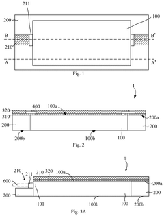
Silicon photonic chip package module based on plastic encapsulation
PatentPendingUS20250291137A1
Innovation
- The proposed silicon photonic chip package module includes a transparent cushioning material layer covering the port of the silicon photonic chip, a plastic encapsulation layer with grooves for fiber optics, and a metal interconnect layer replacing conventional metal wires, allowing direct optical connection to a fiber optic and reducing alignment errors.
Method of manufacturing and packaging silicon photonics integrated circuit dies in wafer form
PatentActiveUS11837509B1
Innovation
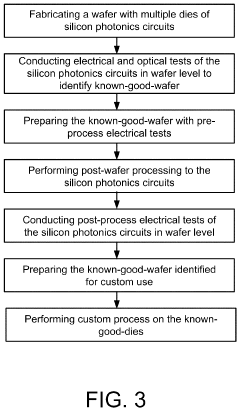
- A method for manufacturing and packaging silicon photonics wafer products that involves fabricating silicon photonics integrated circuits on a silicon-on-insulator wafer, conducting wafer-level testing, and performing post-wafer processing to create known-good-wafers for custom optical-electrical modules, including flip-bonding functional chips and aligning fiber arrays for light coupling, enabling efficient assembly of optical-electrical modules.
Supply Chain and Manufacturing Considerations
The integration of silicon photonics into consumer electronics presents unique supply chain and manufacturing challenges that require careful consideration. Traditional electronics manufacturing ecosystems must adapt to accommodate optical components with significantly different handling requirements. The supply chain for silicon photonics in consumer applications remains fragmented, with specialized vendors providing discrete components such as lasers, modulators, and photodetectors, while system integration often occurs at separate facilities.
Material sourcing represents a critical bottleneck in scaling silicon photonics for mass consumer markets. High-purity silicon wafers with specific optical properties demand specialized manufacturing processes that currently limit production capacity. Additionally, the integration of III-V materials for light sources introduces complexity in material procurement and quality control. These constraints have created a supply chain vulnerability that manufacturers must address through strategic partnerships and vertical integration initiatives.
Manufacturing processes for silicon photonics packaging require unprecedented precision, with alignment tolerances measured in submicron dimensions. This necessitates specialized equipment investments that significantly exceed those of conventional electronics assembly. The industry has begun adopting modified semiconductor manufacturing techniques, including automated optical alignment systems and specialized die bonding equipment, to improve throughput and yield rates. However, these adaptations remain costly and technically challenging to implement at consumer electronics production scales.
Testing and quality assurance present additional manufacturing hurdles. Unlike electronic components that can be rapidly tested through electrical probing, optical components require more complex characterization procedures. This extends production cycles and increases costs. Leading manufacturers have developed parallel testing methodologies and automated optical inspection systems to mitigate these challenges, though standardization across the industry remains limited.
Scalability concerns persist as consumer electronics manufacturers attempt to transition from low-volume, high-margin applications to mass-market products. Current manufacturing approaches that succeed for datacenter applications prove economically unviable at consumer price points. The industry is exploring novel packaging architectures, including optical interposers and polymer waveguide technologies, to reduce assembly complexity and enable higher throughput manufacturing processes compatible with existing consumer electronics production lines.
Geographical distribution of manufacturing capabilities presents strategic considerations. While design expertise for silicon photonics remains concentrated in North America and Europe, manufacturing capacity has shifted predominantly to East Asia. This geographic separation introduces supply chain vulnerabilities that companies must address through redundant sourcing strategies and localized manufacturing partnerships to ensure resilience against disruptions.
Thermal Management Strategies
Thermal management represents a critical challenge in silicon photonics packaging for consumer electronics, particularly as devices continue to shrink while processing requirements increase. The integration of photonic components with electronic circuits generates significant heat that must be efficiently dissipated to maintain optimal performance and reliability. Current thermal management strategies in silicon photonics packaging employ a multi-layered approach addressing both active and passive cooling mechanisms.
Passive cooling techniques form the foundation of thermal management in silicon photonics packages. These include the strategic use of high thermal conductivity materials such as diamond-filled epoxies and copper-tungsten alloys for heat spreaders. Advanced thermal interface materials (TIMs) with enhanced thermal conductivity properties are being deployed between the photonic chip and heat sink to minimize thermal resistance. Additionally, optimized package designs incorporating thermal vias and embedded heat pipes help create efficient thermal pathways from heat sources to the package exterior.
Active cooling solutions complement passive approaches when dealing with high-power applications. Thermoelectric coolers (TECs) are increasingly integrated into silicon photonic packages to provide localized cooling for temperature-sensitive components like lasers and modulators. Micro-fluidic cooling channels, though still emerging in consumer applications, offer promising thermal management capabilities by circulating cooling fluids directly through or adjacent to photonic components. These active solutions enable precise temperature control necessary for wavelength stability in photonic devices.
Thermal simulation and modeling have become essential tools in the development cycle of silicon photonics packages. Computational fluid dynamics (CFD) and finite element analysis (FEA) allow designers to predict thermal hotspots and optimize heat dissipation pathways before physical prototyping. These simulation approaches have significantly reduced development time and improved thermal performance in the latest generation of photonic packages for consumer electronics.
Industry leaders are exploring novel thermal management approaches including phase-change materials that absorb heat during state transitions and graphene-based thermal solutions that leverage the material's exceptional thermal conductivity. 3D packaging techniques that optimize component placement based on thermal considerations are also gaining traction, allowing heat-generating components to be strategically positioned near cooling interfaces.
The consumer electronics market presents unique thermal challenges for silicon photonics, including strict constraints on package size, weight, and power consumption. Thermal management strategies must therefore balance performance with these practical limitations. As silicon photonics continues to penetrate mainstream consumer devices like smartphones, AR/VR headsets, and wearables, thermal management innovations will remain a key enabler for successful market adoption and product reliability.
Unlock deeper insights with PatSnap Eureka Quick Research — get a full tech report to explore trends and direct your research. Try now!
Generate Your Research Report Instantly with AI Agent
Supercharge your innovation with PatSnap Eureka AI Agent Platform!