Evaluating Market Dynamics in Silicon Photonics Packaging
SEP 29, 20259 MIN READ
Generate Your Research Report Instantly with AI Agent
PatSnap Eureka helps you evaluate technical feasibility & market potential.
Silicon Photonics Packaging Background and Objectives
Silicon photonics packaging represents a critical technological frontier that has evolved significantly over the past two decades. Initially emerging as a niche technology in the early 2000s, silicon photonics has transformed from laboratory experiments to commercial viability, with packaging solutions playing an increasingly vital role in this evolution. The fundamental objective of silicon photonics packaging is to create cost-effective, reliable interfaces between photonic integrated circuits (PICs) and external optical and electrical components while maintaining signal integrity and operational stability.
The technology trajectory has been marked by several pivotal advancements, including the transition from manual assembly to automated packaging processes, the development of wafer-level packaging techniques, and the integration of optical and electrical interconnects in increasingly compact form factors. These developments have been driven by the growing demand for higher bandwidth, lower power consumption, and reduced latency in data communication systems.
Current technological trends in silicon photonics packaging focus on addressing key challenges such as optical coupling efficiency, thermal management, hermetic sealing, and alignment precision at the micron and sub-micron levels. The industry is witnessing a shift toward standardization of packaging platforms and interfaces, which aims to reduce manufacturing complexity and enable broader adoption across various application domains.
The primary technical objectives for silicon photonics packaging development include achieving higher integration density, improving coupling efficiency between optical fibers and on-chip waveguides, enhancing reliability under varying environmental conditions, and significantly reducing packaging costs which currently represent up to 80% of the total module cost. Additionally, there is a growing emphasis on developing packaging solutions compatible with existing semiconductor manufacturing infrastructure to leverage economies of scale.
Looking forward, the silicon photonics packaging roadmap is increasingly aligned with emerging applications beyond traditional data centers and telecommunications, including LiDAR systems for autonomous vehicles, biosensors for medical diagnostics, and quantum computing. These diverse application requirements are driving the development of specialized packaging solutions tailored to specific performance metrics and operational environments.
The convergence of silicon photonics with electronic integration through advanced packaging technologies such as 2.5D and 3D integration represents a frontier that promises to overcome current bandwidth bottlenecks while enabling new system architectures. This technological evolution is expected to continue accelerating as market demands for higher data rates and more efficient computing solutions intensify across multiple industries.
Market Demand Analysis for Silicon Photonics Solutions
The silicon photonics market is experiencing unprecedented growth, driven by increasing data center demands, telecommunications infrastructure expansion, and emerging applications in sensing and medical diagnostics. Current market assessments value the global silicon photonics market at approximately 2.5 billion USD in 2023, with projections indicating a compound annual growth rate (CAGR) of 23-25% through 2030, potentially reaching 11-12 billion USD by the end of the decade.
Data centers represent the largest market segment, accounting for roughly 60% of silicon photonics applications. This dominance stems from the technology's ability to address critical challenges in high-speed data transmission, power consumption reduction, and space optimization. Major cloud service providers including Amazon Web Services, Microsoft Azure, and Google Cloud are actively implementing silicon photonics solutions to manage exponentially growing data traffic while controlling operational costs.
The telecommunications sector constitutes approximately 25% of the market share, with particular emphasis on 5G infrastructure deployment and preparation for 6G technologies. Network operators are increasingly adopting silicon photonics for both long-haul and metropolitan area networks, recognizing benefits in bandwidth capacity and energy efficiency compared to traditional copper-based solutions.
Consumer electronics applications, though currently representing only about 8% of the market, show promising growth potential. Industry analysts anticipate significant adoption in high-end smartphones, augmented reality devices, and autonomous vehicle systems within the next 3-5 years, potentially reshaping market distribution.
Regionally, North America leads with approximately 40% market share, followed by Asia-Pacific at 35% and Europe at 20%. However, the Asia-Pacific region demonstrates the fastest growth trajectory, particularly in China, Taiwan, and Singapore, where substantial investments in manufacturing infrastructure and research capabilities are accelerating market expansion.
Customer demand patterns reveal increasing emphasis on integrated packaging solutions rather than discrete components. End users consistently prioritize three key factors: cost reduction through economies of scale, improved thermal management capabilities, and standardization of interfaces. Survey data indicates that 78% of potential adopters cite packaging costs as their primary barrier to implementation, while 65% express concerns about long-term reliability in varied operating environments.
The silicon photonics packaging market faces a significant supply-demand imbalance, with current production capacity meeting only about 70% of market demand. This gap is expected to persist through at least 2025, creating both challenges and opportunities for market entrants and established players alike. Pricing trends reflect this dynamic, with average selling prices declining at approximately 15% annually despite strong demand, driven by manufacturing improvements and increasing competition.
Technical Challenges in Silicon Photonics Packaging
Silicon photonics packaging represents one of the most significant bottlenecks in the commercialization and widespread adoption of silicon photonics technology. The fundamental challenge stems from the dimensional mismatch between optical fibers (typically 125μm in diameter) and silicon waveguides (approximately 0.5μm wide). This disparity necessitates precise alignment with sub-micron accuracy, creating substantial manufacturing complexities.
Coupling efficiency remains a persistent technical hurdle, with current solutions often introducing 3-5dB of insertion loss per coupling point. This loss significantly impacts overall system performance, particularly in applications requiring multiple I/O connections. Various coupling approaches—including edge coupling, grating couplers, and evanescent coupling—each present distinct trade-offs between coupling efficiency, bandwidth, polarization sensitivity, and manufacturing complexity.
Temperature sensitivity poses another critical challenge. Silicon photonics devices typically exhibit a high thermo-optic coefficient, causing wavelength shifts of approximately 0.1nm/°C. This thermal sensitivity necessitates either precise temperature control systems or athermal design approaches, both adding complexity and cost to packaging solutions.
Hermetic sealing requirements further complicate packaging processes. Photonic integrated circuits (PICs) must be protected from environmental contaminants while maintaining optical transparency at fiber interface points. Traditional electronic packaging methods often prove inadequate for these specialized requirements, necessitating novel approaches.
Scalability for high-volume manufacturing represents perhaps the most significant barrier to widespread commercial adoption. Current packaging processes remain largely manual or semi-automated, with throughput rates significantly lower than electronic packaging counterparts. Alignment procedures typically require active monitoring during assembly, dramatically increasing cycle times and production costs.
Testing methodologies present additional challenges, as conventional electronic testing approaches cannot adequately verify optical functionality. This necessitates specialized optical testing equipment and procedures, further complicating the manufacturing process and increasing costs.
Material compatibility issues arise when integrating photonic components with electronic elements in hybrid assemblies. Coefficient of thermal expansion (CTE) mismatches between silicon, polymers, and metals can induce stress and misalignment during temperature cycling, potentially degrading performance over time.
Standardization remains underdeveloped compared to electronic packaging, with limited industry consensus on interface specifications, testing protocols, and quality metrics. This lack of standardization impedes supply chain development and increases design complexity for system integrators.
Current Packaging Solutions and Methodologies
01 Advanced packaging technologies for silicon photonics
Silicon photonics packaging has evolved with advanced technologies to address integration challenges. These include flip-chip bonding, through-silicon vias (TSVs), and wafer-level packaging that enable higher density integration while maintaining optical alignment precision. These packaging solutions help overcome thermal management issues and reduce signal loss at interfaces, which are critical for maintaining performance in high-speed optical communication systems.- Advanced packaging technologies for silicon photonics: Silicon photonics packaging has evolved with advanced technologies that enable efficient integration of optical and electronic components. These technologies include flip-chip bonding, through-silicon vias (TSVs), and wafer-level packaging that facilitate high-density integration while maintaining optical alignment precision. Advanced packaging solutions address thermal management challenges and enable scalable manufacturing processes for silicon photonic devices.
- Optical coupling and alignment solutions: Efficient optical coupling between silicon photonic chips and external optical fibers or waveguides is critical for system performance. Various coupling techniques have been developed, including edge coupling, grating couplers, and spot-size converters that minimize insertion losses. Precision alignment methods and passive alignment structures are implemented to maintain optical coupling efficiency during packaging and throughout the device lifetime.
- Integration with electronic components: The integration of silicon photonics with electronic components creates hybrid systems that leverage the advantages of both technologies. Co-packaging approaches include 2.5D and 3D integration using interposers or direct bonding techniques. These integration methods enable high-bandwidth, low-latency communication between optical and electronic domains while addressing challenges related to thermal management and signal integrity.
- Hermetic sealing and environmental protection: Silicon photonic devices require protection from environmental factors that can degrade performance. Hermetic sealing technologies using glass lids, metal caps, or polymer encapsulation provide protection against moisture, dust, and other contaminants. These packaging solutions must maintain optical transparency along light paths while ensuring long-term reliability under various operating conditions.
- Scalable manufacturing and cost reduction strategies: Market dynamics in silicon photonics packaging are driven by the need for scalable manufacturing processes that reduce costs while maintaining performance. Automated assembly techniques, standardized packaging platforms, and wafer-level processing enable high-volume production. Novel materials and design approaches are being developed to simplify packaging requirements and improve yield, addressing key barriers to widespread commercial adoption.
02 Optical coupling and alignment solutions
Efficient optical coupling between photonic components and external optical fibers remains a key challenge in silicon photonics packaging. Various solutions have emerged including edge coupling, grating couplers, and automated active alignment techniques. These approaches aim to minimize coupling losses while enabling scalable manufacturing processes. Innovations in this area focus on maintaining sub-micron alignment precision during assembly and throughout the product lifecycle despite thermal and mechanical stresses.Expand Specific Solutions03 Integration of electronics and photonics
The co-packaging of electronic and photonic components represents a significant market trend in silicon photonics. This integration approach combines CMOS electronics with optical components to reduce power consumption and increase bandwidth density. Heterogeneous integration techniques enable the combination of different material platforms while addressing thermal management challenges. These solutions are particularly valuable for data centers and high-performance computing applications requiring high-bandwidth, energy-efficient interconnects.Expand Specific Solutions04 Scalable manufacturing processes
The silicon photonics market is increasingly focused on developing scalable manufacturing processes to reduce costs and increase production volumes. This includes automated assembly techniques, standardized packaging platforms, and process optimization for high-yield manufacturing. Innovations in this area aim to leverage existing semiconductor manufacturing infrastructure while addressing the unique requirements of optical components. These advancements are critical for enabling mass adoption of silicon photonics technology across various application domains.Expand Specific Solutions05 Emerging applications driving packaging innovation
New application domains are driving innovation in silicon photonics packaging. These include quantum computing, LiDAR for autonomous vehicles, biosensing, and artificial intelligence accelerators. Each application presents unique packaging requirements related to operating conditions, form factors, and performance metrics. The market dynamics are increasingly shaped by these diverse use cases, leading to specialized packaging solutions that address application-specific challenges while maintaining cost-effectiveness and reliability.Expand Specific Solutions
Key Industry Players and Competitive Landscape
Silicon photonics packaging is currently in a growth phase, with the market expected to expand significantly due to increasing demand for high-speed data transmission and energy-efficient computing solutions. The global market size is projected to reach several billion dollars by 2030, driven by applications in data centers, telecommunications, and emerging AI infrastructure. Technologically, the field shows varying maturity levels across different players. Industry leaders like Intel, TSMC, and Huawei have established advanced manufacturing capabilities and integrated solutions, while specialized companies such as Aeponyx and Vanguard Automation are developing innovative packaging approaches. GlobalFoundries and IBM Research are advancing standardization efforts, while academic institutions like Nanyang Technological University and Technical University of Berlin contribute fundamental research. The ecosystem is evolving toward more automated, scalable packaging solutions to address cost and volume production challenges.
Taiwan Semiconductor Manufacturing Co., Ltd.
Technical Solution: TSMC has developed a comprehensive silicon photonics packaging platform that leverages their advanced semiconductor manufacturing expertise. Their approach focuses on 3D heterogeneous integration, combining silicon photonics dies with electronic ICs using their advanced packaging technologies like Chip-on-Wafer-on-Substrate (CoWoS) and Integrated Fan-Out (InFO). TSMC's silicon photonics packaging solutions incorporate specialized through-silicon vias (TSVs) designed specifically for optical-electronic integration, minimizing signal degradation. Their manufacturing process includes precision optical alignment techniques achieving sub-micron accuracy for fiber-to-chip coupling. TSMC has also developed specialized materials and processes for hermetic sealing of photonic components while maintaining optical transparency where needed. Their packaging solutions address thermal management challenges through innovative heat dissipation structures that protect temperature-sensitive photonic elements while efficiently cooling electronic components.
Strengths: World-class semiconductor manufacturing capabilities; established ecosystem partnerships with design tool providers; advanced heterogeneous integration technologies. Weaknesses: Relatively newer entrant to silicon photonics compared to some specialized competitors; challenges in scaling optical alignment processes to match their electronic manufacturing volumes.
Huawei Technologies Co., Ltd.
Technical Solution: Huawei has developed proprietary silicon photonics packaging technologies focused on telecommunications and data center applications. Their approach centers on a modular packaging platform that enables flexible integration of various optical components with electronic control circuits. Huawei's silicon photonics modules utilize specialized optical coupling techniques that achieve high efficiency while maintaining compatibility with standard fiber optic connectors. Their packaging solutions incorporate automated passive alignment methods that significantly reduce assembly costs while maintaining optical performance. Huawei has pioneered the use of polymer waveguides as optical interconnects within their packages, offering lower loss and better thermal stability than traditional approaches. Their silicon photonics packaging also features integrated optical multiplexing/demultiplexing capabilities, enabling high-bandwidth density in compact form factors. Huawei's manufacturing process incorporates specialized hermetic sealing techniques that protect sensitive photonic components while allowing optical signals to pass through designated interfaces.
Strengths: Vertical integration from chip design through system implementation; extensive telecommunications application expertise; cost-effective manufacturing processes optimized for volume production. Weaknesses: Geopolitical challenges affecting global market access; limited third-party ecosystem support compared to more open platforms; relatively higher dependence on proprietary solutions.
Core Patents and Innovations in Photonic Integration
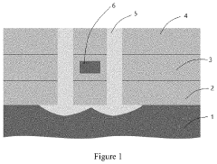
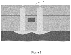
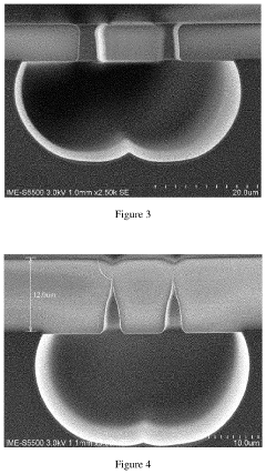
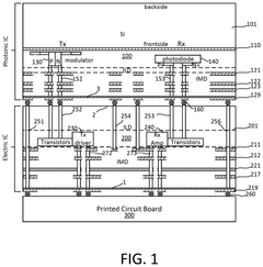
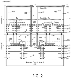
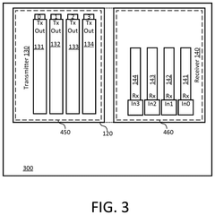
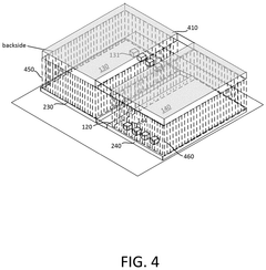
Method for packaging semiconductor structure, packaging structure, and chip
PatentInactiveUS20220308288A1
Innovation
- A method involving plasma-enhanced chemical vapor deposition (PECVD) is used to form a thin silicon oxide film that seals the trench opening without overfilling, leveraging its low step coverage to retain the cavity structure and prevent material blockage, which is then followed by subsequent packaging processes like TSV formation and copper electroplating.
Method and structure for shielding electromagnetic inteference in photonic integrated circuits stacked up electronic integrated circuits
PatentPendingUS20250060545A1
Innovation
- The implementation of through-silicon-vias (TSVs) connected to a conductive layer on the backside of the PIC, forming an electromagnetic shield that terminates electric and magnetic fields, thereby enhancing grounding and reducing crosstalk.
Supply Chain Considerations for Silicon Photonics
The silicon photonics supply chain represents a complex ecosystem that significantly impacts market dynamics in silicon photonics packaging. This intricate network encompasses raw material suppliers, wafer fabrication facilities, packaging houses, testing services, and distribution channels. The supply chain for silicon photonics differs markedly from traditional semiconductor supply chains due to the integration of optical and electronic components, requiring specialized materials and manufacturing processes.
Material sourcing presents a critical consideration, with high-purity silicon, III-V materials for laser integration, and specialty optical coatings being essential components. The limited number of suppliers for these specialized materials creates potential bottlenecks and price volatility. Geographic concentration of these suppliers, predominantly in East Asia, North America, and Western Europe, introduces geopolitical risks that can disrupt availability and pricing.
Manufacturing capacity constraints represent another significant challenge. The fabrication of silicon photonics devices requires specialized foundry services with capabilities for both electronic and photonic integration. Currently, only a limited number of foundries worldwide possess these capabilities, creating production bottlenecks during periods of high demand. This limitation directly impacts packaging costs and lead times.
Vertical integration strategies are increasingly being adopted by major industry players to mitigate supply chain vulnerabilities. Companies like Intel, IBM, and Cisco have invested in developing in-house capabilities across multiple supply chain segments. This trend toward vertical integration may reshape competitive dynamics by providing integrated players with greater control over costs, quality, and innovation timelines.
The emergence of specialized packaging service providers represents a notable trend in the ecosystem. These companies focus exclusively on the complex packaging requirements of silicon photonics, offering expertise in fiber coupling, hermetic sealing, and thermal management. Their specialized knowledge helps address technical challenges while potentially reducing costs through economies of scale and process optimization.
Standardization efforts across the supply chain are gradually gaining momentum, with industry consortia working to establish common specifications for materials, interfaces, and testing protocols. These initiatives aim to reduce fragmentation, improve interoperability, and ultimately lower costs throughout the supply chain. However, the pace of standardization remains relatively slow compared to the rapid technological advancement in the field.
Standardization Efforts in Photonic Packaging
The standardization landscape in silicon photonics packaging represents a critical foundation for industry-wide adoption and scalability. Currently, several international organizations are spearheading efforts to establish common frameworks, including the IEEE P3186 working group focused specifically on silicon photonic integrated circuits, and the IEC's Technical Committee 86 addressing fiber optic systems more broadly. These initiatives aim to create unified specifications for optical interfaces, thermal management protocols, and reliability testing methodologies.
Industry consortia play an equally important role in standardization efforts. The Consortium for On-Board Optics (COBO) has developed multi-source agreements (MSAs) for on-board optical modules, while the Optical Internetworking Forum (OIF) continues to advance interoperability standards for photonic integrated circuits. These collaborative approaches have successfully established preliminary standards for fiber attachment techniques, electrical interface specifications, and thermal design considerations.
The photonics ecosystem has recognized standardization as a market accelerator rather than a constraint. By establishing common platforms, manufacturers can reduce development costs while customers benefit from interchangeable components and simplified integration processes. Recent progress includes the development of standardized test procedures for waveguide coupling efficiency and standardized packaging form factors that accommodate various chip architectures.
Geographical differences in standardization approaches present both challenges and opportunities. European initiatives, often led by Photonics21 and EPIC (European Photonics Industry Consortium), emphasize open platforms and reference designs. Meanwhile, North American efforts frequently focus on application-specific standards driven by data center and telecommunications requirements. Asian standardization bodies, particularly in Japan and China, have concentrated on manufacturing process standardization to support high-volume production capabilities.
Looking forward, emerging standardization priorities include protocols for co-packaged optics, where optical engines are integrated directly with electronic switches or processors. Additionally, standards for automated assembly processes are gaining traction as the industry moves toward higher production volumes. The development of standardized design kits and process design rules represents another frontier, potentially enabling a more accessible ecosystem for photonic integrated circuit designers across various application domains.
The economic impact of standardization cannot be overstated, with market analysts projecting that widely adopted standards could reduce packaging costs by 30-40% over the next five years, potentially unlocking new application segments previously constrained by cost barriers.
Unlock deeper insights with PatSnap Eureka Quick Research — get a full tech report to explore trends and direct your research. Try now!
Generate Your Research Report Instantly with AI Agent
Supercharge your innovation with PatSnap Eureka AI Agent Platform!