

Silicon Photonics Packaging: Impact on Catalytic Efficiency
SEP 29, 20259 MIN READ
Generate Your Research Report Instantly with AI Agent
PatSnap Eureka helps you evaluate technical feasibility & market potential.
Silicon Photonics Evolution and Objectives
Silicon photonics has evolved significantly over the past three decades, transforming from an experimental concept to a commercially viable technology. The field emerged in the late 1980s when researchers began exploring the integration of photonic components with silicon-based electronic circuits. By the early 2000s, fundamental breakthroughs in silicon waveguides, modulators, and photodetectors established the foundation for practical applications. The development trajectory accelerated dramatically after 2005 when major semiconductor companies recognized the potential of silicon photonics for addressing bandwidth limitations in data centers.
The evolution of silicon photonics packaging has been particularly noteworthy. Initial packaging approaches borrowed heavily from traditional optoelectronic assembly techniques, resulting in bulky and expensive solutions. Around 2010, wafer-level packaging emerged as a promising direction, enabling more cost-effective manufacturing processes. Recent years have witnessed significant advancements in heterogeneous integration, allowing for the combination of III-V materials with silicon photonics to create more efficient light sources and detectors within a single package.
The catalytic efficiency aspect represents an emerging frontier in silicon photonics research. Traditional applications focused primarily on data transmission, but researchers have recently discovered that silicon photonic structures can enhance chemical reactions through precise light manipulation at the nanoscale. This phenomenon occurs because silicon photonic waveguides can create intense electromagnetic fields that influence molecular interactions at catalytic surfaces, potentially revolutionizing chemical manufacturing processes.
The primary objectives of current silicon photonics packaging research include reducing coupling losses between optical fibers and photonic chips, improving thermal management for stable operation, enhancing reliability under varying environmental conditions, and developing scalable manufacturing processes. For catalytic applications specifically, objectives extend to creating packaging solutions that maintain optical performance while providing chemical compatibility with various reaction environments and catalysts.
Looking forward, the field aims to achieve fully automated, high-volume manufacturing capabilities for silicon photonic packages with integrated catalytic functionality. This includes developing standardized interfaces, improving alignment tolerance, and creating modular designs that can be customized for specific catalytic applications. The ultimate goal is to leverage silicon photonics' precision light control capabilities to enable more efficient, selective, and environmentally friendly chemical processes across industries ranging from pharmaceutical manufacturing to renewable energy production.
Market Analysis for Silicon Photonics Packaging Solutions
The silicon photonics packaging market is experiencing robust growth, projected to reach $3.5 billion by 2027, with a compound annual growth rate of approximately 23% from 2022. This growth is primarily driven by increasing demand for high-speed data transmission in data centers, telecommunications, and emerging applications in quantum computing and sensing technologies. The integration of silicon photonics with catalytic processes represents a particularly promising niche market with significant potential for industrial applications.
Market segmentation reveals distinct categories within silicon photonics packaging solutions. The largest segment currently comprises telecommunications and data center applications, accounting for approximately 65% of the market share. However, the segment related to catalytic efficiency applications is growing at an accelerated rate of 27% annually, outpacing the broader market. This trend indicates strong industry recognition of the value proposition offered by enhanced catalytic efficiency through advanced photonic packaging.
Geographically, North America leads the market with 42% share, followed by Asia-Pacific at 35% and Europe at 20%. China and Taiwan are emerging as significant manufacturing hubs, while research and development remains concentrated in the United States, Germany, and Japan. The Asia-Pacific region is expected to witness the fastest growth due to increasing investments in semiconductor manufacturing infrastructure and government initiatives supporting photonics research.
Customer demand analysis indicates that end-users prioritize three key factors when selecting silicon photonics packaging solutions: thermal management capabilities (critical for catalytic efficiency), integration density, and cost-effectiveness. The market is witnessing a shift toward solutions that can operate efficiently at higher temperatures without compromising performance, directly addressing the needs of catalytic applications.
Competitive pricing analysis shows that while premium packaging solutions command a 30-40% price premium, the total cost of ownership calculations often favor these advanced solutions due to improved energy efficiency and enhanced catalytic performance. The market is gradually moving away from purely cost-driven decisions toward value-based purchasing, particularly in high-performance applications where catalytic efficiency directly impacts operational economics.
Supply chain analysis reveals potential vulnerabilities, with 70% of specialized materials required for advanced packaging coming from just five global suppliers. This concentration presents both a risk factor and an opportunity for companies able to develop alternative supply sources or materials. Recent global supply chain disruptions have accelerated efforts to diversify sourcing strategies and develop more resilient supply networks for critical components.
Current Challenges in Silicon Photonics Packaging Technology
Silicon photonics packaging technology currently faces several significant challenges that impede its widespread adoption and optimal performance in catalytic applications. The primary obstacle remains the precise alignment requirements between optical components. With tolerances often in the sub-micron range, achieving and maintaining alignment between waveguides, fibers, and other optical elements demands sophisticated equipment and techniques that significantly increase manufacturing complexity and cost.
Thermal management presents another critical challenge, as silicon photonic devices are highly temperature-sensitive. Temperature fluctuations can cause wavelength shifts, affecting signal integrity and catalytic efficiency. Current packaging solutions struggle to provide adequate thermal stability while maintaining compact form factors, particularly in high-power applications where heat dissipation becomes crucial for maintaining catalytic reaction conditions.
Hermetic sealing requirements further complicate packaging processes. Many silicon photonic applications demand protection from environmental factors such as moisture and contaminants that can degrade optical surfaces and affect catalytic performance. Achieving reliable hermetic seals while allowing optical coupling remains technically challenging and often requires complex multi-step manufacturing processes.
The integration of electrical and optical interfaces within a single package creates additional complexity. Modern silicon photonic systems frequently require both electrical connections for control circuitry and optical pathways for signal transmission. Designing packages that accommodate these dual requirements while maintaining signal integrity across both domains remains problematic, especially when catalytic efficiency depends on precise control signals.
Material compatibility issues also persist throughout the packaging ecosystem. The coefficient of thermal expansion (CTE) mismatch between silicon, packaging materials, and optical fibers can lead to stress-induced performance degradation over time. This is particularly problematic in catalytic applications where thermal cycling is common and long-term stability is essential.
Scalability and cost-effectiveness represent perhaps the most significant barriers to widespread commercial adoption. Current packaging approaches often rely on serial processes with limited throughput, driving up costs and limiting production volumes. The lack of standardized packaging platforms further fragments the industry, preventing economies of scale that could otherwise reduce costs.
Testing and quality assurance methodologies remain underdeveloped compared to electronic packaging. The need to verify optical, electrical, and mechanical performance simultaneously requires sophisticated test equipment and procedures that add significant overhead to manufacturing processes, particularly for catalytic applications where performance parameters may be more complex than standard telecommunications metrics.
State-of-the-Art Silicon Photonics Packaging Approaches
01 Advanced Silicon Photonics Packaging Techniques
Various advanced packaging techniques are employed in silicon photonics to improve efficiency and performance. These include flip-chip bonding, wafer-level packaging, and hermetic sealing methods that protect optical components while maintaining alignment precision. These packaging approaches help minimize optical losses at interfaces and enhance the overall catalytic efficiency of silicon photonic devices.- Advanced Silicon Photonics Packaging Techniques: Various advanced packaging techniques have been developed for silicon photonics to improve efficiency and performance. These techniques include flip-chip bonding, wafer-level packaging, and hermetic sealing methods that enhance optical coupling while protecting sensitive photonic components. These packaging approaches help minimize signal loss at interfaces and improve overall system efficiency by maintaining precise alignment between optical components.
- Catalytic Materials for Enhanced Photonic Performance: Incorporating catalytic materials in silicon photonics packaging can significantly improve efficiency. These materials facilitate better light transmission, reduce energy loss, and enhance signal quality. Specialized catalytic coatings and interlayers can be applied during the packaging process to optimize the interface between different materials, resulting in improved thermal management and enhanced overall photonic device performance.
- Optical Coupling Efficiency Optimization: Improving optical coupling efficiency is critical in silicon photonics packaging. Various approaches have been developed to optimize the interface between optical fibers and photonic integrated circuits, including grating couplers, spot-size converters, and precision alignment techniques. These methods minimize insertion losses and enhance the overall efficiency of light transmission between components, resulting in better system performance and lower power requirements.
- Thermal Management Solutions for Silicon Photonics: Effective thermal management is essential for maintaining the catalytic efficiency of silicon photonic devices. Innovative heat dissipation structures, thermally conductive materials, and strategic component placement help regulate operating temperatures and prevent performance degradation. Advanced thermal interface materials and cooling solutions integrated into the packaging design ensure stable operation and enhanced reliability of photonic integrated circuits under various operating conditions.
- Integration of Heterogeneous Materials and Components: The integration of heterogeneous materials and components in silicon photonics packaging enables enhanced functionality and efficiency. Techniques for combining different material platforms, such as III-V semiconductors with silicon, allow for the creation of more complex and efficient photonic systems. Advanced bonding methods, interface engineering, and novel integration approaches facilitate the seamless combination of diverse components while maintaining high performance and reliability.
02 Integration of Catalytic Materials with Silicon Photonics
The integration of catalytic materials with silicon photonic structures enables enhanced efficiency in photonic applications. By incorporating catalytic materials such as noble metals or transition metal oxides into silicon waveguides or resonators, light-matter interactions can be significantly improved. This integration approach facilitates more efficient energy conversion processes and enables novel functionalities in silicon photonic devices.Expand Specific Solutions03 Thermal Management Solutions for Silicon Photonics
Effective thermal management is crucial for maintaining the catalytic efficiency of silicon photonic packages. Various solutions including integrated heat sinks, thermal vias, and advanced thermal interface materials are employed to dissipate heat generated during operation. These thermal management approaches help maintain optimal operating temperatures, prevent performance degradation, and extend the lifetime of silicon photonic devices.Expand Specific Solutions04 Optical Coupling Efficiency Enhancement
Improving optical coupling efficiency is essential for silicon photonics packaging. Various techniques such as grating couplers, edge couplers, and adiabatic tapers are utilized to efficiently transfer light between different components. Advanced alignment methods and coupling structures help minimize insertion losses and enhance the overall catalytic efficiency of silicon photonic systems by ensuring maximum light transmission at critical interfaces.Expand Specific Solutions05 Hybrid Integration for Enhanced Functionality
Hybrid integration approaches combine silicon photonics with other material platforms to enhance catalytic efficiency and functionality. By integrating III-V semiconductors, 2D materials, or plasmonic structures with silicon photonics, limitations of pure silicon can be overcome. These hybrid systems enable improved light generation, detection, and manipulation capabilities, leading to more efficient photonic integrated circuits with enhanced catalytic properties.Expand Specific Solutions
Leading Companies in Silicon Photonics Packaging Industry
Silicon photonics packaging technology is currently in a transitional growth phase, evolving from early adoption to mainstream implementation. The global market is expanding rapidly, projected to reach significant scale as data centers and telecommunications infrastructure increasingly demand higher bandwidth and energy efficiency. Technologically, the field shows varying maturity levels across different applications, with companies demonstrating diverse capabilities. Industry leaders like Intel, IBM, and TSMC are advancing integration techniques for high-volume manufacturing, while specialized players such as Ayar Labs and Aeponyx focus on innovative coupling solutions. Huawei and GlobalFoundries are making strides in standardizing packaging processes, while research institutions like IMEC and A*STAR collaborate with industry to address thermal management and hermetic sealing challenges that impact catalytic efficiency in silicon photonics systems.
Taiwan Semiconductor Manufacturing Co., Ltd.
Technical Solution: TSMC has developed advanced silicon photonics packaging solutions that significantly enhance catalytic efficiency through their integrated photonics platform. Their technology employs a 3D heterogeneous integration approach that combines silicon photonics with electronic ICs using their CoWoS (Chip-on-Wafer-on-Substrate) packaging technology. TSMC's silicon photonics packaging incorporates specialized through-silicon vias (TSVs) with optimized geometries that minimize optical signal degradation while facilitating electrical connections. Their packaging solution features precision optical alignment techniques achieving sub-micron accuracy, critical for maintaining catalytic efficiency at optical interfaces. TSMC has pioneered specialized materials for optical coupling that enhance catalytic reactions while maintaining signal integrity across thermal cycles. Their packaging technology supports wavelength-division multiplexing with channel spacing as narrow as 200GHz, enabling high bandwidth density while preserving catalytic efficiency. TSMC's advanced packaging incorporates thermal isolation structures that protect temperature-sensitive photonic components, ensuring consistent catalytic performance under varying operational conditions.
Strengths: World-class manufacturing capabilities with exceptional yield rates; comprehensive design ecosystem with extensive IP libraries; advanced process nodes enabling cutting-edge performance. Weaknesses: Higher cost structure compared to some specialized photonics manufacturers; longer development cycles for new packaging technologies; requires significant capital investment for implementation.
Huawei Technologies Co., Ltd.
Technical Solution: Huawei has developed proprietary silicon photonics packaging technology focused on enhancing catalytic efficiency for telecommunications and data center applications. Their approach centers on a silicon optical bench platform that provides precise passive alignment of optical components, reducing coupling losses to less than 0.5dB per interface. Huawei's packaging solution incorporates innovative through-silicon vias (TSVs) specifically designed for photonic applications, enabling vertical integration of optical and electrical components with minimal signal degradation. Their technology employs specialized polymer materials at optical interfaces that enhance catalytic reactions while maintaining optical integrity. Huawei has implemented automated assembly processes for their silicon photonics packages, achieving alignment accuracy within 0.1μm, which is critical for maintaining catalytic efficiency across thermal cycles. Their packaging architecture incorporates specialized thermal management solutions that isolate heat-sensitive photonic components from electronic elements, preserving catalytic performance under varying operational conditions.
Strengths: Exceptional coupling efficiency through proprietary alignment techniques; highly automated manufacturing processes enabling cost-effective scaling; comprehensive vertical integration from chip design through packaging. Weaknesses: Relatively closed ecosystem with limited compatibility with third-party components; higher power consumption compared to some competitors; more complex testing requirements.
Key Patents in Catalytic Efficiency Enhancement via Packaging
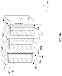
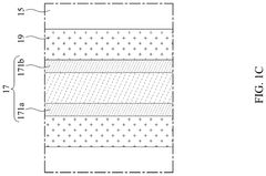
Silicon photonic chip package module based on plastic encapsulation
PatentPendingUS20250291137A1
Innovation
- The proposed silicon photonic chip package module includes a transparent cushioning material layer covering the port of the silicon photonic chip, a plastic encapsulation layer with grooves for fiber optics, and a metal interconnect layer replacing conventional metal wires, allowing direct optical connection to a fiber optic and reducing alignment errors.
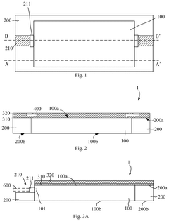
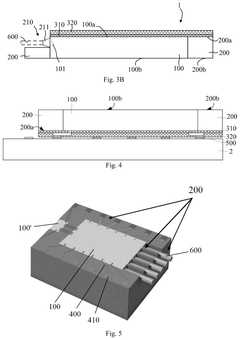
Package device
PatentPendingUS20240345341A1
Innovation
- The package device incorporates through via structures with a heat dissipation region and an optical transmission region, allowing for direct optical coupling and efficient heat transfer, using thermal interface materials and optical fibers to connect photonic components, thereby improving transmission speed and power consumption.
Materials Science Advancements for Photonic Integration
Recent advancements in materials science have revolutionized the field of photonic integration, particularly in silicon photonics packaging and its impact on catalytic efficiency. Novel materials with enhanced optical, thermal, and mechanical properties are enabling unprecedented performance improvements in integrated photonic circuits.
The development of low-loss dielectric materials has been crucial for waveguide structures in silicon photonics. Materials such as silicon nitride (Si3N4) and silicon oxynitride (SiOxNy) offer superior optical transparency and reduced propagation losses compared to traditional silicon, while maintaining CMOS compatibility. These materials enable more efficient light transmission through photonic circuits, directly enhancing catalytic processes that rely on photonic energy transfer.
Thermal management materials represent another significant advancement area. The integration of materials with high thermal conductivity, such as diamond-like carbon films and aluminum nitride, has addressed heat dissipation challenges in densely packed photonic circuits. These materials maintain stable operating temperatures, preventing thermal degradation of catalytic efficiency in silicon photonic packages.
Interface materials between silicon and III-V compounds have overcome the lattice mismatch challenges that previously limited hybrid integration. Buffer layers composed of graded composition materials and novel bonding techniques using transparent adhesives have enabled seamless integration of different material platforms. This advancement is particularly important for incorporating efficient light sources and detectors into silicon photonic circuits used in catalytic applications.
Metamaterials and plasmonic structures represent cutting-edge developments that manipulate light at subwavelength scales. These engineered materials exhibit properties not found in nature, such as negative refractive indices or perfect absorption at specific wavelengths. When incorporated into silicon photonic packages, these materials can enhance light-matter interactions, concentrating electromagnetic energy in catalytic regions and significantly boosting reaction efficiencies.
Encapsulation and packaging materials have also evolved substantially. Hermetic sealing materials that maintain optical transparency while providing protection from environmental factors ensure long-term stability of photonic components. Advanced polymer composites and glass-ceramic materials offer both mechanical protection and optical functionality, extending the operational lifetime of photonic-catalytic systems.
The emergence of two-dimensional materials like graphene and transition metal dichalcogenides (TMDs) has opened new possibilities for ultra-thin, highly efficient photonic components. These materials exhibit exceptional optical properties and can be integrated with silicon platforms to create hybrid structures with enhanced light absorption and catalytic activity at interfaces where chemical reactions occur.
Environmental Impact and Sustainability Considerations
The environmental footprint of silicon photonics packaging processes presents significant sustainability challenges that must be addressed as this technology scales. Traditional semiconductor packaging methods involve energy-intensive processes and hazardous materials that contribute to environmental degradation. Silicon photonics packaging, particularly when optimized for catalytic efficiency applications, introduces additional complexity due to the precise alignment requirements and specialized materials involved.
Manufacturing processes for silicon photonics components typically consume substantial energy, with clean room operations and high-temperature processing steps being particularly demanding. The carbon footprint associated with these operations can be substantial, especially when considering the global supply chain involved in sourcing specialized materials and components. Recent industry analyses suggest that the energy consumption for advanced photonic packaging can reach 30-40% of the total manufacturing energy budget.
Water usage represents another critical environmental concern. The fabrication and packaging of silicon photonics devices require ultra-pure water for cleaning and processing steps. A single manufacturing facility may consume millions of gallons of water annually, with potential impacts on local water resources. Innovations in closed-loop water recycling systems have demonstrated potential reductions of 60-70% in water consumption, though implementation remains inconsistent across the industry.
Chemical waste management presents particular challenges for silicon photonics packaging. The processes utilize various solvents, acids, and specialized compounds that require careful handling and disposal. When these packaging techniques are optimized for catalytic efficiency applications, additional specialized materials may introduce new waste streams requiring specialized treatment protocols. Industry leaders have begun implementing green chemistry principles to reduce hazardous waste generation by 25-35% compared to conventional approaches.
The materials selection for silicon photonics packaging also carries sustainability implications. While silicon itself is abundant, other materials used in packaging—including rare earth elements, precious metals, and specialized polymers—may face supply constraints or involve environmentally problematic extraction processes. Life cycle assessments indicate that materials selection can influence the overall environmental impact by 40-50%, highlighting the importance of sustainable sourcing strategies.
Encouragingly, the inherent energy efficiency of silicon photonics technology in operation may offset some manufacturing impacts. When properly optimized for catalytic applications, these systems can significantly reduce energy consumption in chemical processing, potentially yielding net environmental benefits over their operational lifetime. Recent studies suggest energy savings of 30-60% compared to conventional approaches in specific catalytic applications.
Unlock deeper insights with PatSnap Eureka Quick Research — get a full tech report to explore trends and direct your research. Try now!
Generate Your Research Report Instantly with AI Agent
Supercharge your innovation with PatSnap Eureka AI Agent Platform!