Silicon Photonics Packaging in EV Battery Manufacturing
SEP 29, 20259 MIN READ
Generate Your Research Report Instantly with AI Agent
Patsnap Eureka helps you evaluate technical feasibility & market potential.
Silicon Photonics in EV Battery Manufacturing: Background and Objectives
Silicon photonics, an emerging technology that integrates optical components with silicon-based electronics, has evolved significantly over the past two decades. Initially developed for telecommunications and data centers, this technology is now finding applications in various sectors including automotive and energy storage systems. The integration of silicon photonics in electric vehicle (EV) battery manufacturing represents a convergence of advanced optoelectronics and energy storage technologies.
The historical trajectory of silicon photonics began in the early 2000s with basic research on silicon-based optical waveguides and modulators. By the 2010s, commercial applications emerged primarily in high-speed data transmission. Recent advancements have miniaturized photonic components and improved their integration with electronic circuits, enabling new applications beyond data communications, including sensing and monitoring systems relevant to battery manufacturing.
In the context of EV battery production, silicon photonics offers promising capabilities for real-time monitoring and quality control. The technology enables precise measurements of critical parameters during battery cell assembly, formation, and testing processes. This includes thermal profiling, structural integrity assessment, and chemical composition analysis—all crucial for ensuring battery performance, safety, and longevity.
The technical objectives for silicon photonics in EV battery manufacturing focus on several key areas. First, developing robust packaging solutions that can withstand harsh manufacturing environments while maintaining optical alignment precision. Second, creating integrated sensing systems capable of monitoring multiple battery parameters simultaneously with high accuracy. Third, establishing cost-effective manufacturing processes that enable mass production of silicon photonic components for the EV industry.
Current trends indicate a growing interest in distributed sensing networks within battery production lines, where multiple photonic sensors work in concert to provide comprehensive monitoring. Additionally, there is movement toward integrating artificial intelligence with photonic sensing systems to enable predictive quality control and early fault detection during manufacturing.
The ultimate goal is to leverage silicon photonics technology to enhance battery manufacturing precision, reduce defect rates, extend battery lifespan, and improve safety profiles. This aligns with broader industry objectives to reduce EV battery costs while increasing energy density and reliability—key factors in accelerating electric vehicle adoption globally.
As the EV market continues its rapid expansion, the development of advanced manufacturing technologies becomes increasingly critical. Silicon photonics represents a promising technological pathway to address current limitations in battery production processes and quality assurance methods.
Market Analysis for Silicon Photonics in EV Battery Production
The electric vehicle (EV) battery manufacturing market is experiencing unprecedented growth, driven by the global shift towards sustainable transportation. Within this expanding sector, silicon photonics technology presents a significant opportunity for innovation in battery production processes. Current market projections indicate that the global EV battery market will reach approximately $133 billion by 2027, with a compound annual growth rate exceeding 18% from 2022 to 2027.
Silicon photonics integration in battery manufacturing represents an emerging niche with substantial growth potential. The technology enables precise optical sensing and monitoring systems that can dramatically improve quality control in battery cell production. Market research suggests that advanced manufacturing technologies like silicon photonics could reduce battery production costs by up to 30% while simultaneously improving energy density and safety parameters.
The demand for silicon photonics in EV battery production is primarily driven by three key factors. First, the increasing pressure to reduce battery costs to achieve price parity with internal combustion engine vehicles. Second, the growing emphasis on battery safety and reliability following high-profile thermal runaway incidents. Third, the push for higher energy density batteries to extend EV range capabilities.
Regional market analysis reveals that Asia-Pacific currently dominates the EV battery manufacturing landscape, with China, Japan, and South Korea collectively accounting for over 70% of global production capacity. However, significant investments in North America and Europe are rapidly changing this distribution, with both regions expected to double their market share by 2025.
Consumer demand patterns indicate a clear preference for EVs with longer ranges and faster charging capabilities, directly influencing battery manufacturing priorities. This consumer-driven trend is creating market pull for advanced process control technologies that can produce more uniform and higher-performing battery cells.
The total addressable market for silicon photonics in battery manufacturing is estimated to reach $2.5 billion by 2028. Early adopters are primarily tier-one battery manufacturers who supply to premium EV brands, where the cost-benefit ratio of implementing advanced optical inspection and monitoring systems is most favorable.
Market penetration analysis shows that silicon photonics technology has currently achieved less than 5% penetration in battery manufacturing processes, indicating substantial room for growth. The technology adoption curve suggests an inflection point within the next 24-36 months as successful pilot implementations demonstrate return on investment through improved yield rates and reduced scrap.
Current Challenges in Silicon Photonics Packaging for EV Applications
Silicon photonics packaging in EV battery manufacturing faces significant technical hurdles that impede widespread adoption. The integration of optical components with electronic systems presents unique challenges due to the harsh automotive environment. Temperature fluctuations in EVs, ranging from -40°C to over 125°C, create thermal expansion mismatches between silicon photonic chips and their substrates, leading to optical misalignment and performance degradation over time.
Hermetic sealing represents another major obstacle, as silicon photonic devices are highly sensitive to moisture and contaminants. Traditional hermetic packaging techniques often involve high-temperature processes that can damage temperature-sensitive photonic components. The automotive-grade reliability requirements demand solutions that maintain hermeticity throughout the vehicle's lifecycle while withstanding vibration, shock, and thermal cycling.
Coupling efficiency between optical fibers and silicon waveguides remains problematic in production environments. Current coupling methods achieve only 40-60% efficiency in mass production settings, resulting in significant signal loss. This inefficiency necessitates higher-power optical sources, increasing system cost and energy consumption—critical factors in energy-constrained EV applications.
Manufacturing scalability presents a formidable barrier to cost reduction. Current silicon photonics packaging processes rely heavily on manual alignment and specialized equipment, with cycle times of 5-10 minutes per device. This contrasts sharply with electronic component assembly, which operates at sub-second cycle times. The precision requirements for optical alignment (typically <0.1μm) exceed standard SMT equipment capabilities by an order of magnitude.
Cost structures remain prohibitive for automotive applications. While electronic components benefit from economies of scale, silicon photonic packaging costs remain high at $50-200 per device, primarily due to specialized materials, precision alignment requirements, and low yields. EV manufacturers typically target component costs below $10 for similar functionality.
Integration with existing automotive manufacturing processes poses additional challenges. Current silicon photonics packaging techniques often require clean room environments and specialized handling procedures incompatible with standard automotive assembly lines. This creates logistical complications and increases manufacturing complexity.
Testing and quality assurance methodologies for packaged silicon photonic devices lack standardization in automotive contexts. Unlike electronic components with established test protocols, optical testing requires specialized equipment and expertise not readily available in automotive supply chains. This complicates quality control and increases verification costs throughout the production process.
Current Packaging Solutions for Silicon Photonics in EV Batteries
01 Optical coupling techniques in silicon photonics packaging
Various optical coupling techniques are employed in silicon photonics packaging to efficiently transfer light between optical components. These include edge coupling, grating couplers, and evanescent coupling methods that minimize insertion loss. Advanced alignment techniques ensure precise positioning of optical components relative to waveguides, which is critical for maintaining signal integrity across the photonic integrated circuit.- Optical coupling techniques in silicon photonics packaging: Various optical coupling techniques are employed in silicon photonics packaging to efficiently transfer light between optical components. These include edge coupling, grating couplers, and evanescent coupling methods that minimize insertion loss. Advanced alignment techniques ensure precise positioning of optical components to maintain signal integrity across interfaces. These coupling solutions address the challenges of mode mismatch between different waveguide structures.
- Thermal management solutions for silicon photonics: Thermal management is critical in silicon photonics packaging to maintain operational stability and reliability. Solutions include integrated heat sinks, thermal vias, and specialized thermal interface materials that efficiently dissipate heat from active components. Temperature control mechanisms help maintain wavelength stability in temperature-sensitive photonic devices. These approaches prevent performance degradation due to thermal variations and extend device lifetime.
- Integration of electronic and photonic components: Hybrid integration approaches combine electronic and photonic components in a single package to achieve high-performance optoelectronic systems. These include 2.5D and 3D integration techniques using interposers, through-silicon vias (TSVs), and flip-chip bonding. Co-packaging of drivers, amplifiers, and control electronics with photonic integrated circuits reduces parasitic effects and improves signal integrity while minimizing form factor.
- Hermetic sealing and environmental protection: Hermetic sealing techniques protect sensitive silicon photonic components from environmental factors such as moisture, dust, and contaminants. Methods include glass lid bonding, metal sealing, and specialized polymer encapsulation that maintain optical transparency where needed. These protection strategies ensure long-term reliability and stability of photonic devices in various operating conditions while maintaining optical access for fiber connections.
- Wafer-level packaging for silicon photonics: Wafer-level packaging techniques enable cost-effective mass production of silicon photonic devices. These approaches include wafer bonding, through-silicon via formation, and collective alignment processes that can be performed at the wafer scale before singulation. Advanced lithography and etching processes create optical pathways and alignment structures directly in the wafer. This methodology significantly reduces packaging costs while improving throughput and yield.
02 Thermal management solutions for silicon photonic packages
Thermal management is crucial in silicon photonics packaging to maintain stable operation of temperature-sensitive photonic components. Solutions include integrated thermoelectric coolers, heat spreaders, and thermal vias that efficiently dissipate heat from active components. These thermal management strategies help prevent wavelength drift in lasers and maintain consistent performance of modulators and detectors across varying operating conditions.Expand Specific Solutions03 Hermetic sealing and protection techniques
Hermetic sealing and protection methods are essential for ensuring the long-term reliability of silicon photonic devices. These techniques include glass lid bonding, metal sealing, and polymer encapsulation that protect sensitive optical components from environmental factors such as moisture, dust, and mechanical stress. Advanced materials and bonding processes are employed to maintain optical alignment while providing robust environmental protection.Expand Specific Solutions04 Integration of electronic and photonic components
The integration of electronic and photonic components in a single package presents unique challenges that require specialized solutions. Approaches include 2.5D and 3D integration techniques, interposer technologies, and through-silicon vias that enable efficient communication between electronic and photonic layers. These integration methods minimize signal latency while addressing the different material requirements and fabrication processes of electronic and photonic components.Expand Specific Solutions05 Fiber attachment and alignment methods
Precise fiber attachment and alignment methods are critical for efficient light coupling between optical fibers and silicon photonic chips. Techniques include passive alignment using V-grooves, active alignment with real-time optical feedback, and self-alignment structures that facilitate high-throughput assembly. Advanced adhesives and welding techniques are used to secure fibers while maintaining alignment stability over temperature variations and mechanical stress.Expand Specific Solutions
Key Industry Players in Silicon Photonics and EV Battery Sectors
Silicon photonics packaging in EV battery manufacturing is emerging as a critical technology intersection, currently in its early growth phase. The market is expanding rapidly, driven by increasing EV adoption and demand for advanced battery management systems. While still evolving, the technology shows promising maturity levels with key players advancing different aspects of the ecosystem. Companies like GlobalFoundries and IBM are developing silicon photonics platforms, while BYD and BYTON are exploring integration into EV battery systems. Specialized firms such as Aeponyx and Vanguard Automation are innovating in optical interconnect solutions. ASE and Dow Silicones contribute essential packaging materials and processes. This competitive landscape reflects a technology transitioning from research to commercial applications, with significant growth potential as EV manufacturing scales globally.
Aeponyx, Inc.
Technical Solution: Aeponyx has developed a specialized silicon photonics packaging solution targeting the unique requirements of EV battery manufacturing environments. Their technology centers around micro-optical-electro-mechanical systems (MOEMS) that combine the benefits of MEMS technology with silicon photonics to create highly miniaturized optical switching and sensing components. Aeponyx's approach utilizes their patented micro-mirror technology to create reconfigurable optical pathways within battery monitoring systems, allowing for adaptive sensing configurations that can be optimized for different battery chemistries and form factors. Their packaging solution incorporates plasmonic structures that enhance optical signal strength while minimizing power consumption, critical for battery-powered applications where energy efficiency is paramount. The company's technology employs wafer-level packaging techniques that hermetically seal optical components while maintaining precise alignment, protecting sensitive elements from the corrosive environment inside battery cells. Aeponyx's solution features integrated optical isolators that prevent back-reflections and cross-talk between sensing channels, ensuring measurement accuracy even in high-vibration automotive environments. Their packaging architecture supports wavelength division multiplexing, enabling multiple sensing functions to share a single optical fiber, significantly reducing wiring complexity throughout the battery pack.
Strengths: Ultra-compact form factor enables integration in space-constrained battery designs; low power consumption minimizes impact on overall battery efficiency; reconfigurable architecture provides flexibility for different battery chemistries. Weaknesses: Limited production capacity may challenge scaling to high-volume automotive requirements; relatively new technology with limited field validation in automotive environments; higher complexity in calibration and maintenance compared to conventional solutions.
BYD Co., Ltd.
Technical Solution: BYD has developed an innovative silicon photonics packaging solution integrated directly into their Blade Battery architecture for electric vehicles. Their approach combines silicon photonics with their proprietary battery cell design to create a comprehensive monitoring system that enhances safety and performance. BYD's technology embeds optical waveguides within the battery pack structure, creating a network of sensors that monitor temperature distribution, structural integrity, and chemical composition in real-time. Their packaging solution utilizes a unique edge-coupling technique that maintains optical alignment despite the thermal expansion and contraction cycles inherent in battery operation. The company has developed specialized optical interfaces that can withstand exposure to electrolyte materials while maintaining signal integrity. BYD's integrated approach places silicon photonic chips at strategic locations throughout the battery pack, connected via radiation-hardened fiber optic pathways that are immune to the electromagnetic interference generated during high-current charging and discharging events. This distributed architecture enables millisecond-level response to thermal events, potentially preventing thermal runaway situations before they become dangerous.
Strengths: Vertical integration with battery manufacturing provides seamless implementation; distributed sensing architecture offers superior spatial resolution for monitoring; direct integration with BYD's battery management system enables immediate protective responses. Weaknesses: Proprietary nature limits compatibility with third-party battery systems; higher manufacturing complexity increases production time; limited track record compared to established photonics solutions.
Critical Patents and Technical Literature Review
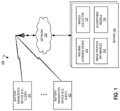
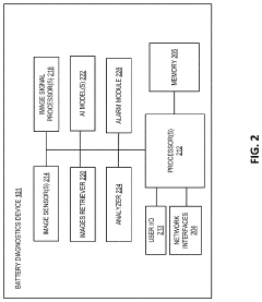
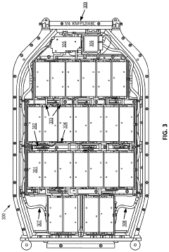
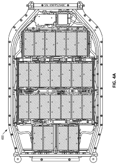
Advanced diagnostics, assembly and service of a high voltage battery using image profiles
PatentInactiveUS20210123870A1
Innovation
- A system that uses high-resolution RGB, thermal, and electromagnetic image profiles to diagnose and assemble battery packs by comparing captured images with reference images, identifying abnormalities, and alerting technicians to stop the assembly line if discrepancies are found, utilizing machine learning models and AI to analyze image data for faulty components.
Thermal interface material coating method for battery cells
PatentPendingUS20230411729A1
Innovation
- A novel TIM coating method using a rotating or moving mechanism with a slot die coater and a meshed substrate with pores to ensure uniform TIM film thickness on battery cells, where the substrate's design, including curvature radius, thickness, and pore size, along with controlled fluid flow and rotation/motion speed, allows for even distribution and adherence of TIM fluid, forming a laterally uniform film.
Thermal Management Strategies for Silicon Photonics in EV Environments
Thermal management represents a critical challenge in the integration of silicon photonics technology within electric vehicle battery manufacturing systems. The operating environment of EVs presents unique thermal constraints, with temperature fluctuations ranging from -40°C to over 85°C depending on geographic location, season, and vehicle operating conditions. Silicon photonic devices, particularly those incorporating sensitive components like lasers and modulators, demonstrate significant performance variations with temperature changes, affecting wavelength stability, optical coupling efficiency, and overall signal integrity.
Current thermal management approaches for silicon photonics in EV applications can be categorized into passive and active solutions. Passive strategies include specialized packaging materials with high thermal conductivity, such as diamond-filled composites and ceramic substrates, which facilitate efficient heat dissipation without additional power requirements. These materials create thermal pathways that draw heat away from sensitive optical components while maintaining mechanical stability across temperature cycles.
Active thermal management solutions incorporate thermoelectric coolers (TECs) and micro-fluidic cooling channels directly integrated into photonic packages. These systems provide precise temperature control but introduce additional power consumption considerations that must be balanced against the energy constraints of EV platforms. Advanced implementations utilize phase-change materials (PCMs) that absorb or release thermal energy during state transitions, effectively dampening temperature fluctuations during rapid operational changes.
Hermetic packaging techniques have emerged as particularly valuable for EV applications, providing both thermal stability and protection against humidity and contaminants. Glass-to-silicon anodic bonding and gold-tin eutectic sealing create robust thermal interfaces while maintaining hermeticity, extending the operational lifetime of photonic components in harsh automotive environments.
Recent innovations focus on thermally-aware design methodologies that incorporate athermal waveguide structures and temperature-compensated optical circuits. These approaches utilize materials with opposing thermo-optic coefficients to create inherently temperature-stable photonic elements. Silicon nitride and polymer overlays on silicon waveguides demonstrate significantly reduced thermal sensitivity compared to conventional silicon-only designs.
Simulation-driven thermal management has become increasingly important, with finite element modeling tools enabling accurate prediction of thermal gradients across complex photonic packages. These computational approaches allow designers to identify and mitigate potential hotspots before physical prototyping, reducing development cycles and improving reliability in production environments.
The integration of distributed temperature sensors within photonic packages represents another advancement, enabling real-time thermal monitoring and adaptive control strategies. These systems can dynamically adjust cooling parameters based on actual operating conditions, optimizing power consumption while maintaining optimal performance parameters for silicon photonic components in variable EV environments.
Supply Chain Resilience and Manufacturing Scalability
The integration of silicon photonics packaging into EV battery manufacturing faces significant supply chain challenges that require strategic planning for long-term resilience and scalability. Currently, the supply chain for silicon photonics components remains fragmented, with key materials and specialized equipment concentrated among a limited number of suppliers primarily located in North America, Europe, and East Asia. This geographic concentration creates vulnerability to regional disruptions, as evidenced during recent global supply chain crises.
Manufacturing scalability presents both challenges and opportunities for silicon photonics in EV battery applications. The transition from low-volume, high-precision manufacturing typical of photonics to the high-volume production required for the automotive sector necessitates substantial process innovation. Current silicon photonics packaging techniques often involve manual alignment steps that are difficult to scale, creating bottlenecks in production throughput.
Vertical integration strategies are emerging among leading EV manufacturers seeking to secure critical components. Companies like Tesla and BYD have begun investing in photonics capabilities to reduce dependency on external suppliers. Simultaneously, tier-one automotive suppliers are forming strategic partnerships with photonics specialists to develop robust supply networks that can withstand market fluctuations and geopolitical tensions.
Material sourcing represents another critical dimension of supply chain resilience. Silicon itself is abundant, but specialized materials required for photonics packaging—including rare earth elements for certain optical components—face supply constraints. Developing alternative materials and recycling processes will be essential for long-term sustainability of silicon photonics in EV applications.
Standardization efforts across the industry could significantly enhance manufacturing scalability. Currently, the lack of unified standards for silicon photonics interfaces and packaging specifications increases production complexity and costs. Industry consortia including automotive and photonics stakeholders are working to establish common standards that would facilitate higher volume production and interchangeability of components.
Regional manufacturing capabilities are diversifying as governments recognize the strategic importance of advanced semiconductor and photonics technologies. Initiatives like the CHIPS Act in the United States and similar programs in Europe and Asia are creating incentives for domestic production capacity, potentially reducing supply chain vulnerabilities while increasing global manufacturing capacity for silicon photonics components used in EV battery systems.
Unlock deeper insights with Patsnap Eureka Quick Research — get a full tech report to explore trends and direct your research. Try now!
Generate Your Research Report Instantly with AI Agent
Supercharge your innovation with Patsnap Eureka AI Agent Platform!