

Silicon Photonics Packaging: Semiconductor Material Advancements
SEP 29, 202510 MIN READ
Generate Your Research Report Instantly with AI Agent
PatSnap Eureka helps you evaluate technical feasibility & market potential.
Silicon Photonics Evolution and Objectives
Silicon photonics emerged in the late 1980s as researchers began exploring the integration of optical components with silicon-based electronic circuits. The initial breakthrough came with the development of silicon waveguides that could effectively guide light, opening possibilities for on-chip optical communication. Throughout the 1990s, fundamental components such as modulators and photodetectors were gradually developed, though with limited performance compared to traditional optical materials.
The early 2000s marked a significant acceleration in silicon photonics development, driven by increasing data center bandwidth demands and telecommunications needs. Intel's demonstration of a silicon modulator operating at gigahertz speeds in 2004 represented a pivotal moment, proving that silicon could indeed serve as a viable platform for high-speed optical communications. This period also saw the emergence of specialized foundry services for silicon photonics, enabling broader research and commercial exploration.
Between 2010 and 2020, silicon photonics transitioned from research laboratories to commercial applications, with companies like Intel, IBM, and Luxtera (later acquired by Cisco) introducing products incorporating silicon photonic components. The technology demonstrated its value in data centers, high-performance computing, and telecommunications infrastructure, offering advantages in bandwidth, energy efficiency, and integration potential with electronic systems.
The packaging of silicon photonic devices has evolved alongside the core technology, transitioning from rudimentary laboratory setups to increasingly sophisticated commercial solutions. Early packaging approaches focused primarily on basic functionality, with little emphasis on cost-effectiveness or manufacturability at scale. As the technology matured, packaging solutions began addressing critical challenges such as fiber-to-chip coupling, thermal management, and hermetic sealing.
Current objectives in silicon photonics packaging center on several key areas. First, achieving higher integration density to accommodate more optical functionality in smaller footprints. Second, developing cost-effective packaging solutions that maintain performance while enabling mass production. Third, improving coupling efficiency between optical fibers and on-chip waveguides to minimize signal loss. Fourth, enhancing thermal management capabilities to ensure stable operation across varying conditions.
Looking forward, the field aims to develop packaging technologies that can support emerging applications in quantum computing, biosensing, and neuromorphic computing. Additionally, there is growing interest in heterogeneous integration approaches that combine silicon with other semiconductor materials to overcome silicon's inherent limitations in light emission and detection. The ultimate goal remains creating fully integrated electro-optical systems that seamlessly merge electronic and photonic functionalities while meeting stringent requirements for reliability, performance, and cost-effectiveness.
Market Demand Analysis for Silicon Photonics
The silicon photonics market is experiencing unprecedented growth driven by increasing demands for high-speed data transmission, cloud computing infrastructure, and telecommunications advancements. Current market projections indicate that the global silicon photonics market is expected to reach $3.5 billion by 2025, with a compound annual growth rate of approximately 23% between 2020 and 2025. This remarkable growth trajectory is primarily fueled by data center applications, which currently account for over 60% of the market share.
The surge in data traffic, particularly with the expansion of 5G networks and the increasing adoption of Internet of Things (IoT) devices, has created substantial demand for higher bandwidth and more energy-efficient data transmission solutions. Silicon photonics technology addresses these needs by enabling optical interconnects that significantly outperform traditional copper-based connections in terms of speed, power consumption, and transmission distance.
Telecommunications providers represent another significant market segment, as they seek to upgrade their infrastructure to handle increasing data loads while minimizing energy consumption. The ability of silicon photonics to integrate seamlessly with existing CMOS manufacturing processes makes it particularly attractive for telecom applications, offering a path to cost-effective scaling of optical networks.
Consumer electronics manufacturers are also showing growing interest in silicon photonics for next-generation devices. The potential for silicon photonics to enable faster data transfer in consumer products, from smartphones to augmented reality devices, represents an emerging market segment with substantial growth potential in the coming years.
Healthcare and biomedical applications constitute a smaller but rapidly expanding market segment. Silicon photonic biosensors offer unprecedented sensitivity for diagnostic applications, while photonic integrated circuits enable compact, portable medical devices with advanced capabilities. Market analysts predict this segment could grow at over 30% annually through 2025.
Geographically, North America currently leads the silicon photonics market with approximately 40% market share, followed by Europe and Asia-Pacific. However, the Asia-Pacific region is expected to witness the highest growth rate over the next five years, driven by increasing investments in telecommunications infrastructure and data centers in countries like China, Japan, and South Korea.
The demand for advanced semiconductor materials for silicon photonics packaging is particularly strong, as packaging represents one of the most significant challenges in commercializing silicon photonics technology. Materials that can address thermal management issues, reduce coupling losses, and enable more efficient integration with electronic components are seeing especially high demand growth.
Current Packaging Challenges and Limitations
Silicon photonics packaging faces significant challenges that currently limit its widespread adoption and commercial viability. The integration of optical components with electronic systems demands precise alignment tolerances at the submicron level, which is substantially more stringent than traditional electronic packaging requirements. This precision is critical because even minor misalignments can cause substantial optical coupling losses, dramatically reducing system performance. The challenge is further complicated by the need to maintain this alignment across varying thermal conditions, as different materials expand and contract at different rates.
Thermal management represents another major obstacle in silicon photonics packaging. Optical components are highly sensitive to temperature variations, which can alter refractive indices and cause wavelength shifts in optical signals. Current packaging solutions struggle to efficiently dissipate heat while maintaining the optical integrity of the system. This is particularly problematic in high-power applications where thermal gradients can significantly impact performance and reliability.
The hermetic sealing requirements for photonic components add another layer of complexity. Unlike electronic components that can often function in standard environments, photonic elements must be protected from moisture, dust, and other contaminants that can scatter light or degrade optical surfaces. Current sealing technologies often involve complex processes that are difficult to scale for high-volume manufacturing.
Material compatibility issues further complicate packaging solutions. The integration of diverse materials—silicon, III-V semiconductors, polymers, and metals—creates challenges in terms of adhesion, thermal expansion matching, and long-term reliability. Many current bonding techniques introduce stress at material interfaces, potentially leading to delamination or fracture over time.
Manufacturing scalability remains a significant limitation. Many current packaging approaches rely on serial processes with high precision equipment, resulting in low throughput and high costs. The industry lacks standardized, high-volume manufacturing processes comparable to those in the electronic semiconductor industry, creating a bottleneck in production scaling.
Testing and quality control present additional challenges. Unlike electronic components that can be tested through electrical probing, photonic components require specialized optical testing methods that are more complex and time-consuming. This increases production costs and limits throughput in manufacturing environments.
Finally, the cost structure of current packaging solutions remains prohibitively high for many applications. The specialized equipment, precision alignment processes, and low yields contribute to packaging costs that can represent up to 80% of the total device cost. This economic barrier significantly limits the adoption of silicon photonics technology in cost-sensitive markets and applications.
Current Packaging Solutions and Techniques
01 Silicon photonics integration with semiconductor materials
Integration of silicon photonics with various semiconductor materials enables enhanced functionality in photonic integrated circuits. These approaches combine silicon's optical properties with other semiconductors' electrical and optical characteristics to create high-performance optoelectronic devices. The integration methods include heterogeneous bonding, monolithic growth, and hybrid assembly techniques that maintain optical alignment while accommodating different material properties.- Silicon photonics integration with semiconductor materials: Silicon photonics technology integrates optical components with semiconductor materials to create photonic integrated circuits. These circuits combine the light-guiding properties of silicon with traditional semiconductor manufacturing techniques to enable high-speed data transmission. The integration allows for efficient coupling between optical and electronic components while maintaining compatibility with CMOS fabrication processes, resulting in cost-effective and scalable photonic devices.
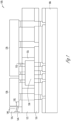
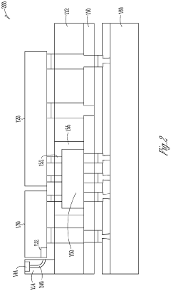
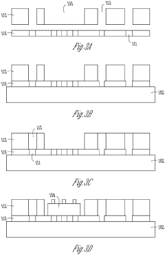
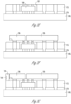
- Advanced packaging techniques for silicon photonics: Advanced packaging techniques for silicon photonics involve methods to protect and connect optical components while maintaining optical alignment precision. These techniques include flip-chip bonding, through-silicon vias (TSVs), and wafer-level packaging that enable 3D integration of photonic and electronic components. The packaging solutions address thermal management challenges and provide hermetic sealing to protect sensitive optical elements while facilitating efficient coupling to optical fibers and other external components.
- Semiconductor materials for photonic applications: Various semiconductor materials are utilized in silicon photonics to enhance functionality and performance. While silicon forms the foundation for waveguides and passive components, other materials like germanium, III-V compounds, and silicon-germanium alloys are incorporated to enable active functions such as light emission, detection, and modulation. These materials are strategically integrated through techniques such as epitaxial growth, wafer bonding, or direct deposition to create hybrid photonic devices with optimized optical and electrical properties.
- Optical coupling and alignment solutions: Optical coupling and alignment solutions address the critical challenge of efficiently transferring light between different components in silicon photonic systems. These solutions include edge couplers, grating couplers, and spot-size converters that minimize insertion losses at interfaces between waveguides, fibers, and other optical elements. Advanced alignment techniques utilize passive alignment features, active alignment processes, and specialized packaging structures to maintain precise optical paths while accommodating thermal expansion and mechanical stress.
- Thermal management and reliability considerations: Thermal management and reliability are crucial aspects of silicon photonics packaging due to the temperature sensitivity of optical components. Solutions include specialized heat spreaders, thermal interface materials, and strategic placement of components to manage heat dissipation. Packaging designs incorporate stress isolation features to minimize thermomechanical stresses that could affect optical alignment. Hermetic sealing techniques protect against environmental factors while allowing for long-term stability and reliability of the photonic devices under various operating conditions.
02 Advanced packaging techniques for silicon photonics
Various packaging methodologies have been developed specifically for silicon photonic devices to maintain optical alignment while providing electrical connectivity and thermal management. These include flip-chip bonding, through-silicon vias (TSVs), interposers, and wafer-level packaging approaches. These techniques address the unique challenges of photonic packaging such as precise alignment tolerances, optical coupling efficiency, and protection of sensitive optical surfaces.Expand Specific Solutions03 Optical coupling solutions for silicon photonics
Efficient optical coupling between silicon photonic chips and external optical components is critical for system performance. Various coupling solutions have been developed including grating couplers, edge couplers, and mode converters that facilitate low-loss transitions between different waveguide geometries. These coupling structures are designed to maximize light transmission while accommodating manufacturing tolerances and environmental variations.Expand Specific Solutions04 Thermal management in silicon photonic packages
Thermal management is crucial for silicon photonic devices as temperature variations can affect optical properties and device performance. Advanced thermal solutions include integrated thermoelectric coolers, heat spreaders, and thermally conductive materials that efficiently dissipate heat while maintaining optical alignment. These approaches help maintain stable operating temperatures for temperature-sensitive components such as lasers, modulators, and wavelength-selective devices.Expand Specific Solutions05 Optical communication systems using silicon photonics
Silicon photonics enables high-bandwidth optical communication systems through integration of multiple optical components on a single chip. These systems incorporate modulators, detectors, multiplexers, and waveguides to transmit and process optical signals at high data rates. The packaging solutions for these systems address challenges related to fiber attachment, electrical interconnects, and system integration while maintaining signal integrity across optical and electrical domains.Expand Specific Solutions
Key Industry Players and Ecosystem
Silicon photonics packaging is currently in a growth phase, with the market expected to reach significant expansion due to increasing demand for high-speed data transmission and energy-efficient computing solutions. The competitive landscape features established semiconductor giants like Intel, TSMC, and GlobalFoundries investing heavily in silicon photonics integration technologies, alongside specialized players such as Xscape Photonics and Aeponyx developing innovative solutions. Research institutions including IBM Research and the Institute of Microelectronics of Chinese Academy of Sciences are advancing material science for improved photonic-electronic integration. Technology maturity varies across applications, with data center interconnects being more mature while quantum computing applications remain experimental. Companies like Huawei and Marvell are focusing on packaging solutions that address thermal management and coupling efficiency challenges, which remain critical barriers to widespread commercial adoption.
Taiwan Semiconductor Manufacturing Co., Ltd.
Technical Solution: TSMC has developed comprehensive silicon photonics packaging solutions that leverage their advanced semiconductor manufacturing expertise. Their approach includes a 300mm silicon photonics platform that integrates germanium photodetectors, silicon modulators, and passive components with CMOS electronics. TSMC's packaging technology utilizes advanced through-silicon vias (TSVs) and micro-bumps to create 3D integrated photonic-electronic systems with minimal interconnect losses. Their manufacturing process incorporates precision alignment techniques that maintain sub-micron positioning accuracy between optical components, critical for maintaining signal integrity. TSMC has pioneered specialized materials for optical coupling interfaces that reduce insertion losses between fiber connections and on-chip waveguides. Their silicon photonics packaging includes hermetic sealing technologies specifically designed to protect sensitive optical components while maintaining thermal stability[4][7]. Recent advancements include their integrated silicon photonics platform that supports wavelength division multiplexing (WDM) with up to 8 channels per waveguide, significantly increasing bandwidth density in data center applications.
Strengths: World-class semiconductor manufacturing infrastructure; established ecosystem of design tools and IP; ability to leverage advanced node technologies for photonics integration; high-volume production capabilities. Weaknesses: Relatively newer entrant to silicon photonics compared to specialized players; challenges in optimizing processes simultaneously for both electronic and photonic components; higher initial investment requirements for customers.
Intel Corp.
Technical Solution: Intel has developed advanced silicon photonics packaging solutions that integrate optical components with CMOS electronics on a single chip. Their technology uses a hybrid integration approach where III-V materials (like InP) are bonded to silicon waveguides to create efficient light sources. Intel's Co-Packaged Optics (CPO) platform combines silicon photonics with ASICs in the same package, significantly reducing power consumption and increasing bandwidth density. Their manufacturing process includes wafer-level integration of optical components and automated assembly techniques that maintain sub-micron alignment precision. Intel has also pioneered techniques for thermal management in silicon photonics packages, using specialized materials to mitigate thermal expansion mismatches between optical and electronic components[1][3]. Recent advancements include their 400G DR4+ silicon photonics transceivers that utilize advanced packaging to achieve higher data rates while maintaining compatibility with existing fiber infrastructure.
Strengths: Industry-leading manufacturing capabilities with high-volume production expertise; vertical integration from design to fabrication; mature ecosystem for photonics-electronics co-design. Weaknesses: Higher cost structure compared to specialized photonics manufacturers; proprietary technology approach may limit broader industry adoption; thermal management challenges in dense integration scenarios remain.
Critical Materials Innovations and Patents
Photonics chips and semiconductor products having angled optical fibers
PatentActiveUS20230127056A1
Innovation
- The development of PIC chips with substrates featuring grooves angled at 30 to 60 degrees, preferably 45 degrees, along the edges to accommodate optical fibers, allowing for increased edge utilization and efficient optical signal transmission by positioning fibers within these grooves, thereby enhancing data density and communication capabilities.
Semiconductor assembly with waveguide and glass substrate
PatentPendingEP4191307A1
Innovation
- The use of laser-based technology for integrating photonic integrated circuits, electronic integrated circuits, and substrates with low-loss coupling, including laser-made glass-to-glass bonds and embedded waveguides formed through laser direct writing, addresses these challenges by minimizing coupling loss and enabling high-voltage compatibility.
Supply Chain Considerations
The silicon photonics supply chain presents unique challenges and opportunities that significantly impact the advancement of semiconductor materials for photonic packaging. Material sourcing for silicon photonics requires specialized suppliers capable of delivering high-purity silicon, III-V compounds, and various optical materials with exceptional consistency. The fragmented nature of this supply chain creates vulnerabilities, as critical components often rely on limited supplier networks concentrated in specific geographic regions.
Manufacturing capacity represents another critical consideration, with specialized foundry services for silicon photonics remaining less developed than traditional CMOS fabrication. The integration of photonic and electronic components demands hybrid manufacturing approaches that few facilities worldwide can support at scale. This manufacturing bottleneck creates potential constraints as market demand accelerates, particularly for advanced packaging solutions requiring precise material specifications.
Quality control across the supply chain introduces additional complexity, as optical performance depends on material purity and structural precision at nanometer scales. Variations in material composition can dramatically affect optical transmission characteristics, requiring sophisticated inspection and testing protocols throughout the supply chain. These quality assurance requirements add cost and time to production cycles, influencing material selection decisions.
Geopolitical factors increasingly shape supply chain strategies for silicon photonics materials. Trade restrictions, export controls, and intellectual property considerations affect access to specialized materials and manufacturing capabilities. Companies developing advanced silicon photonics packaging solutions must navigate these constraints through diversified sourcing strategies and strategic partnerships with material suppliers across multiple regions.
Sustainability considerations are gaining prominence in supply chain decisions. The environmental impact of rare materials used in photonic applications, energy-intensive manufacturing processes, and end-of-life recyclability all influence material selection and packaging design. Forward-thinking organizations are developing circular economy approaches for silicon photonics components, including material reclamation and recycling pathways.
Cost management remains a fundamental supply chain challenge, with specialized materials for silicon photonics commanding premium prices compared to conventional semiconductor materials. Economies of scale have not yet fully materialized for many photonic materials, creating cost barriers to widespread adoption. Strategic supply chain partnerships and vertical integration initiatives offer potential pathways to cost reduction while maintaining material quality specifications essential for photonic performance.
Environmental Impact and Sustainability
The environmental impact of silicon photonics packaging represents a critical consideration as this technology continues to advance. Traditional semiconductor manufacturing processes are known for their significant ecological footprint, including high energy consumption, water usage, and hazardous chemical utilization. Silicon photonics offers potential improvements in this regard, particularly through material advancements that enable more sustainable manufacturing and operational practices.
Recent developments in semiconductor materials for silicon photonics packaging have focused on reducing rare earth element dependencies. These materials, while essential for certain photonic applications, often involve environmentally damaging extraction processes. New composite materials and alternative dopants are emerging that maintain performance characteristics while utilizing more abundant and less environmentally problematic elements.
Energy efficiency represents another substantial environmental benefit of advanced silicon photonics packaging. The integration of photonic circuits with electronic components reduces power consumption by minimizing conversion losses between optical and electrical signals. Material innovations enabling lower-loss optical transmission further enhance this efficiency advantage, potentially reducing data center energy requirements by 30-50% compared to conventional electronic systems.
Manufacturing process improvements accompanying these material advancements also contribute to sustainability. Techniques such as wafer-level packaging reduce material waste significantly compared to traditional die-level approaches. Additionally, new bonding materials designed specifically for silicon photonics applications require lower processing temperatures, thereby reducing energy consumption during manufacturing.
End-of-life considerations have gained increasing attention in semiconductor material research. Recyclability of silicon photonics components presents challenges due to the heterogeneous integration of different materials. Recent advancements include developing more easily separable material interfaces and biodegradable polymers for non-critical packaging elements, improving the overall lifecycle impact of these technologies.
Water usage reduction represents another environmental benefit emerging from material advancements. Traditional semiconductor manufacturing can consume thousands of gallons of ultra-pure water per wafer. New materials and processes designed specifically for silicon photonics packaging have demonstrated potential water usage reductions of up to 40% through more efficient cleaning processes and alternative cooling solutions.
Regulatory compliance and industry standards are increasingly driving sustainability innovations in this field. Materials being developed today must not only meet performance specifications but also conform to regulations such as RoHS and REACH. This regulatory landscape has accelerated research into lead-free solders and halogen-free molding compounds specifically optimized for photonic applications, further reducing the environmental impact of these advanced technologies.
Unlock deeper insights with PatSnap Eureka Quick Research — get a full tech report to explore trends and direct your research. Try now!
Generate Your Research Report Instantly with AI Agent
Supercharge your innovation with PatSnap Eureka AI Agent Platform!