

Silicon Photonics Packaging: Material Advancements and Challenges
SEP 29, 20259 MIN READ
Generate Your Research Report Instantly with AI Agent
PatSnap Eureka helps you evaluate technical feasibility & market potential.
Silicon Photonics Evolution and Objectives
Silicon photonics has evolved significantly since its conceptual inception in the late 1980s, transitioning from theoretical exploration to commercial implementation over three decades. The initial phase focused on fundamental research into silicon's optical properties, with pioneering work demonstrating basic photonic components like waveguides and modulators on silicon substrates. This period established the theoretical foundation but faced significant practical limitations due to silicon's indirect bandgap nature.
The second evolutionary phase, spanning approximately 2000-2010, marked breakthrough developments in hybrid integration techniques. Researchers successfully combined silicon with III-V materials to overcome silicon's inherent limitations in light emission. This period saw the first demonstration of functional silicon photonic circuits integrating multiple components, establishing proof-of-concept for complex photonic integrated circuits (PICs).
From 2010 onwards, silicon photonics entered its commercialization phase, with companies like Intel, IBM, and Luxtera introducing the first market-ready products. Manufacturing processes matured significantly, leveraging existing CMOS infrastructure to achieve cost-effective production at scale. This period witnessed the standardization of design processes and the emergence of foundry services specifically for silicon photonics.
Currently, silicon photonics is experiencing rapid advancement in integration density and functionality, with state-of-the-art chips incorporating thousands of photonic components. The technology has expanded beyond its initial data center applications to telecommunications, sensing, quantum computing, and artificial intelligence accelerators.
The primary technical objectives for silicon photonics packaging advancement center on several critical areas. First is achieving higher integration density while maintaining thermal stability, as heat management remains a significant challenge in densely packed photonic circuits. Second is improving coupling efficiency between optical fibers and on-chip waveguides, which currently represents a major source of signal loss.
Material advancement objectives focus on developing novel materials compatible with silicon that can enhance functionality while maintaining CMOS compatibility. This includes research into silicon-germanium alloys, silicon nitride, and various polymer materials that offer improved optical properties or processing advantages.
Another key objective is standardization of packaging processes to enable high-volume manufacturing with consistent quality and yield. This requires developing robust design methodologies, testing protocols, and quality control measures specific to photonic components.
Looking forward, the field aims to achieve fully integrated electronic-photonic systems on a single chip, with seamless interaction between optical and electronic domains. This convergence represents the ultimate goal of silicon photonics: creating energy-efficient, high-bandwidth computing and communication systems that overcome the limitations of purely electronic approaches.
Market Demand Analysis for Silicon Photonics
The silicon photonics market has experienced remarkable growth in recent years, driven primarily by increasing data center demands for higher bandwidth, lower power consumption, and reduced latency in optical communications. Market research indicates that the global silicon photonics market is projected to grow at a compound annual growth rate of 23% from 2021 to 2026, reaching approximately 3 billion USD by the end of the forecast period.
Data centers represent the largest application segment, accounting for over 40% of the market share. This dominance stems from the exponential growth in cloud computing services and the need for faster data transmission rates. Telecommunications follows as the second-largest segment, where silicon photonics enables high-speed, long-distance data transmission with minimal signal degradation.
Consumer electronics manufacturers are increasingly incorporating silicon photonics technology into their products, particularly for high-speed data transfer applications. The automotive industry has also begun adopting silicon photonics for advanced driver-assistance systems (ADAS) and autonomous driving technologies, where high-bandwidth, low-latency communication is critical.
Geographically, North America leads the market with approximately 35% share, followed by Europe and Asia-Pacific. However, the Asia-Pacific region is expected to witness the highest growth rate during the forecast period due to increasing investments in telecommunications infrastructure and the presence of major semiconductor manufacturing facilities.
The demand for silicon photonics packaging solutions is particularly strong, as packaging represents up to 80% of the total cost of silicon photonic devices. Industry stakeholders are actively seeking advanced materials and packaging techniques that can reduce costs while maintaining or improving performance metrics.
Key market drivers include the growing adoption of cloud services, increasing internet traffic, the proliferation of IoT devices, and the deployment of 5G networks. Additionally, the shift toward edge computing is creating new opportunities for silicon photonics in applications requiring real-time data processing with minimal latency.
Market challenges include high initial investment costs, complex integration requirements, and thermal management issues. The lack of standardization in packaging technologies also presents a significant barrier to widespread adoption, as it increases development costs and time-to-market for new products.
Customer requirements are evolving toward smaller form factors, higher reliability, and improved thermal performance. There is a growing demand for packaging solutions that can withstand harsh environmental conditions while maintaining optical alignment precision over the device lifetime. This has created a significant opportunity for material innovations in adhesives, underfills, and encapsulants specifically designed for silicon photonics applications.
Current Packaging Challenges and Limitations
Silicon photonics packaging faces significant challenges that currently limit its widespread commercial adoption. The primary obstacle remains the precise alignment requirements between optical components. Silicon photonic devices typically require sub-micron alignment accuracy, which is substantially more demanding than traditional electronic packaging. This precision requirement dramatically increases manufacturing complexity and cost, creating a substantial barrier to mass production.
Thermal management presents another critical challenge. Silicon photonic devices are highly temperature-sensitive, with wavelength shifts of approximately 0.1 nm/°C. This sensitivity necessitates sophisticated thermal control mechanisms to maintain operational stability across varying environmental conditions, adding complexity to package design and increasing power consumption.
Material compatibility issues further complicate packaging efforts. The integration of diverse materials—silicon, III-V semiconductors, polymers, and metals—creates thermal expansion mismatches that induce stress and potential failure points during temperature cycling. These mismatches can lead to optical misalignment, performance degradation, and reduced device reliability over time.
Hermetic sealing requirements pose additional difficulties. Optical components are highly sensitive to environmental contaminants such as moisture and particulates, necessitating hermetic packaging solutions. However, traditional hermetic packaging techniques often involve high-temperature processes that can damage temperature-sensitive photonic components, creating a technical contradiction that demands innovative solutions.
Fiber coupling efficiency remains suboptimal in current packaging approaches. The mode size mismatch between standard optical fibers (typically 9-10 μm) and silicon waveguides (approximately 0.5 μm) creates significant coupling losses. While various coupling structures have been developed, including grating couplers and spot-size converters, they add complexity and often introduce wavelength dependencies that limit operational bandwidth.
Scalability challenges persist in current manufacturing processes. Many packaging solutions rely on active alignment techniques that are inherently time-consuming and equipment-intensive. These processes are difficult to parallelize effectively, creating production bottlenecks that increase costs and limit manufacturing throughput.
Testing and quality assurance present unique challenges for photonic packages. Unlike electronic components, which can be comprehensively tested using established electrical probing techniques, photonic devices require specialized optical testing methodologies. The lack of standardized, high-throughput testing protocols increases production costs and complicates quality control procedures, further hindering commercial viability.
Current Material Solutions for Photonic Packaging
01 Advanced Polymer Materials for Silicon Photonics Packaging
Novel polymer materials are being developed specifically for silicon photonics packaging applications. These polymers offer improved thermal stability, optical transparency, and compatibility with semiconductor manufacturing processes. They provide effective encapsulation for photonic integrated circuits while maintaining optical performance. These materials also feature low birefringence and controlled coefficient of thermal expansion to minimize stress on optical components.- Advanced Polymer Materials for Silicon Photonics Packaging: Polymer materials have emerged as crucial components in silicon photonics packaging due to their versatility, thermal stability, and optical properties. These materials are used for encapsulation, waveguide cladding, and optical coupling interfaces. Advanced polymers provide protection against environmental factors while maintaining optical transparency at key wavelengths. Recent developments include thermally stable polymers with controlled coefficient of thermal expansion (CTE) that minimize stress on silicon components during temperature fluctuations, enhancing the reliability and performance of photonic integrated circuits.
- Hermetic Sealing Materials and Techniques: Hermetic sealing materials play a vital role in protecting sensitive silicon photonic components from moisture, contaminants, and environmental degradation. Recent advancements include glass frit bonding materials, metal alloy solders with improved thermal characteristics, and ceramic-based sealing compounds. These materials provide robust environmental protection while maintaining optical alignment precision. Novel approaches combine multiple material layers to achieve both hermeticity and optical transparency at specific wavelengths, extending the operational lifetime of silicon photonic devices in harsh environments.
- Thermal Management Materials for Silicon Photonics: Thermal management is critical in silicon photonics packaging due to the temperature sensitivity of optical components. Advanced thermal interface materials (TIMs) with high thermal conductivity are being developed to efficiently dissipate heat from active photonic components. These include metal-matrix composites, carbon-based materials like graphene and carbon nanotubes, and phase-change materials that provide adaptive thermal management. These materials help maintain stable operating temperatures, prevent wavelength drift in temperature-sensitive devices, and improve overall reliability and performance of silicon photonic systems.
- Optical Coupling Materials and Interfaces: Advanced materials for optical coupling between fibers, waveguides, and photonic integrated circuits represent a significant area of innovation. Index-matching materials with precisely controlled refractive indices minimize insertion losses at interfaces. Novel optical adhesives combine mechanical stability with optical clarity and long-term reliability. Recent developments include gradient-index materials that provide adiabatic mode conversion between different waveguide geometries, and optically clear resins with enhanced resistance to photodegradation. These materials enable more efficient light coupling, reduced signal loss, and improved manufacturing yields in silicon photonic packages.
- Multi-functional Composite Materials for Integrated Packaging: Multi-functional composite materials are emerging as solutions for integrated silicon photonics packaging challenges. These materials combine electrical, optical, thermal, and mechanical functions in a single material system. Examples include ceramic-polymer composites with tailored dielectric and thermal properties, metal-dielectric nanocomposites for electromagnetic shielding while maintaining optical pathways, and glass-ceramic materials with controlled crystallization for specific optical and mechanical properties. These advanced composites enable more compact packaging designs, improved reliability, and enhanced performance by addressing multiple packaging requirements simultaneously.
02 Hermetic Sealing and Thermal Management Materials
Specialized materials for hermetic sealing and thermal management in silicon photonics packages have been developed. These materials provide protection against environmental factors while efficiently dissipating heat generated during operation. Advanced metal alloys, glass frits, and ceramic composites are being utilized to create reliable seals between different package components. These materials maintain their integrity across wide temperature ranges and ensure long-term reliability of photonic devices.Expand Specific Solutions03 Optical Coupling Materials and Interfaces
Innovative materials for optical coupling between silicon photonic chips and external components have been developed. These materials minimize insertion losses at interfaces and maintain signal integrity. Index-matching materials, specialized adhesives, and novel waveguide structures facilitate efficient light transmission between components. These coupling materials are designed to withstand thermal cycling and aging effects while maintaining stable optical performance over the device lifetime.Expand Specific Solutions04 Integration of Novel Substrate Materials
Advanced substrate materials are being incorporated into silicon photonics packaging to enhance performance and reliability. These include specialized ceramics, glass-ceramics, and composite materials that provide improved thermal, mechanical, and electrical properties. The substrates feature precisely engineered thermal expansion characteristics to match silicon photonic chips and reduce stress-induced performance degradation. These materials enable higher integration density and improved signal integrity in photonic systems.Expand Specific Solutions05 Environmentally Resistant Coating Materials
Specialized coating materials have been developed to protect silicon photonic devices from environmental factors. These coatings provide resistance against moisture, chemicals, and mechanical damage while maintaining optical transparency at key wavelengths. Advanced thin-film materials, including modified silicones, fluoropolymers, and inorganic-organic hybrids, offer superior protection without compromising device performance. These coatings can be applied using techniques compatible with standard semiconductor manufacturing processes.Expand Specific Solutions
Key Industry Players and Ecosystem
Silicon photonics packaging is currently in a growth phase, with the market expected to expand significantly due to increasing demand for high-speed data transmission and integrated photonic solutions. The global market size is projected to reach several billion dollars by 2025, driven by applications in data centers, telecommunications, and sensing. Technologically, the field is advancing rapidly but faces challenges in thermal management, optical coupling, and material integration. Leading players like Intel, IBM, and TSMC are making significant investments in silicon photonics packaging technologies, while specialized companies such as Aeponyx and Vanguard Automation are developing innovative solutions for specific applications. Huawei and GlobalFoundries are also expanding their capabilities in this domain, focusing on integration with existing semiconductor manufacturing processes.
Intel Corp.
Technical Solution: Intel has pioneered silicon photonics packaging with their advanced co-packaged optics (CPO) technology that integrates optical I/O directly with ASICs. Their approach focuses on solving thermal challenges through innovative heat dissipation techniques and addressing optical coupling efficiency issues. Intel's silicon photonics platform utilizes hybrid integration of III-V materials with silicon waveguides, achieving data rates exceeding 400 Gbps per channel. They've developed specialized flip-chip bonding techniques that maintain sub-micron alignment precision between optical components while accommodating coefficient of thermal expansion (CTE) mismatches. Intel has also made significant advancements in hermetic sealing technologies using glass frit bonding that maintains optical alignment during temperature cycling, crucial for long-term reliability in data center environments[1][3].
Strengths: Vertical integration capabilities from design to manufacturing; established high-volume manufacturing infrastructure; advanced materials research capabilities. Weaknesses: Higher production costs compared to traditional electronics packaging; thermal management challenges in densely integrated photonic-electronic systems.
Taiwan Semiconductor Manufacturing Co., Ltd.
Technical Solution: TSMC has developed a comprehensive silicon photonics packaging platform that leverages their advanced semiconductor manufacturing expertise. Their approach focuses on 3D heterogeneous integration of photonic and electronic components using their Chip-on-Wafer-on-Substrate (CoWoS) technology. TSMC has pioneered specialized low-temperature bonding techniques that maintain optical alignment while addressing thermal expansion mismatches between different materials. Their packaging solutions incorporate advanced polymer materials with precisely engineered refractive indices to optimize optical coupling efficiency. TSMC has also developed specialized through-silicon vias (TSVs) for photonic applications that minimize signal degradation while providing electrical connectivity between photonic and electronic layers. Their materials research has yielded novel underfill compounds that protect optical interfaces from environmental contaminants while maintaining optical transparency at key wavelengths[2][5].
Strengths: World-class manufacturing precision and quality control; extensive experience with heterogeneous integration; advanced materials characterization capabilities. Weaknesses: Less vertical integration in photonics compared to pure-play photonics companies; challenges in scaling optical alignment processes to high-volume manufacturing.
Critical Patents and Innovations in Packaging Materials
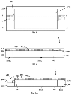
Silicon photonic chip package module based on plastic encapsulation
PatentPendingUS20250291137A1
Innovation
- The proposed silicon photonic chip package module includes a transparent cushioning material layer covering the port of the silicon photonic chip, a plastic encapsulation layer with grooves for fiber optics, and a metal interconnect layer replacing conventional metal wires, allowing direct optical connection to a fiber optic and reducing alignment errors.
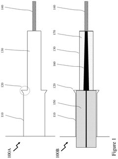
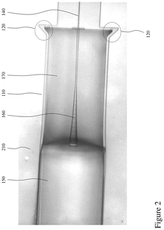
Photonic wire bonding methods and processes for the advanced packaging of photonic devices and systems
PatentPendingUS20250154053A1
Innovation
- The development of photonic wire bonds and photonic wire bonding techniques for packaging discrete integrated optical components, allowing for the formation of optical waveguides that can be directly connected or connected via special structures between optical fibers and integrated optical waveguides, thereby enabling low-cost, low-loss optical interconnections.
Supply Chain Considerations and Constraints
The silicon photonics supply chain presents unique challenges due to the interdisciplinary nature of the technology, combining semiconductor manufacturing with optical components. Material sourcing for silicon photonics packaging remains a critical constraint, particularly for specialized materials such as high-purity silicon wafers, III-V materials for laser integration, and specialty optical polymers. These materials often have limited supplier bases, creating potential bottlenecks in production scaling.
Geographic concentration of key suppliers introduces significant vulnerability to the silicon photonics supply chain. Currently, silicon wafer production is dominated by manufacturers in Japan, Taiwan, and South Korea, while specialty optical materials are often sourced from a small number of suppliers in North America and Europe. This concentration creates risks related to geopolitical tensions, natural disasters, and other regional disruptions.
Manufacturing equipment represents another constraint, as specialized tools for precision alignment and optical testing require substantial capital investment and often face long lead times. The equipment supply chain is similarly concentrated among a few key vendors, primarily in Europe, Japan, and the United States, creating potential capacity limitations as industry demand grows.
Skilled labor shortages present an ongoing challenge throughout the silicon photonics supply chain. The interdisciplinary nature of silicon photonics packaging requires expertise spanning semiconductor processing, optical engineering, and materials science. Universities and training programs have not yet scaled to meet industry demand, creating competition for qualified personnel.
Quality control and standardization issues further complicate supply chain management. Unlike mature semiconductor processes, silicon photonics packaging lacks fully standardized specifications and testing protocols. This inconsistency creates challenges in qualifying new suppliers and ensuring compatibility between components from different vendors.
Regulatory considerations also impact the supply chain, particularly for applications in telecommunications and data centers where compliance with various international standards is required. Environmental regulations affecting certain packaging materials, particularly those containing heavy metals or other restricted substances, may necessitate reformulation or substitution, potentially disrupting established supply chains.
To address these constraints, industry leaders are pursuing vertical integration strategies, developing alternative material sources, and establishing redundant supply chains. Collaborative industry initiatives focused on standardization and workforce development are emerging to address systemic challenges. Additionally, advances in design automation tools may help reduce dependence on specialized materials by enabling more efficient designs with commercially available alternatives.
Environmental Impact and Sustainability Factors
Silicon photonics packaging processes present significant environmental challenges that must be addressed as the industry scales. Traditional packaging methods often involve energy-intensive processes and materials with substantial carbon footprints. The manufacturing of silicon photonic integrated circuits typically requires high-temperature processing, vacuum systems, and specialized clean room environments that consume considerable energy and resources. Additionally, many conventional packaging materials contain hazardous substances such as lead-based solders, which pose environmental risks during production, use, and disposal phases.
Recent material advancements have begun addressing these sustainability concerns. The development of lead-free solders and adhesives specifically designed for photonic applications represents a significant step toward reducing toxic material usage. These alternatives maintain the necessary thermal and mechanical properties while minimizing environmental impact. Similarly, research into biodegradable polymers for optical coupling and protection layers shows promise for reducing end-of-life waste management issues.
Energy efficiency improvements in manufacturing processes are emerging as another critical sustainability factor. Novel low-temperature bonding techniques reduce energy consumption during assembly while maintaining optical alignment precision. Additive manufacturing approaches for certain packaging components minimize material waste compared to traditional subtractive processes, though challenges remain in achieving the necessary precision and optical quality through these methods.
Water usage represents another significant environmental concern in silicon photonics manufacturing. Traditional semiconductor fabrication processes require ultra-pure water in substantial quantities for cleaning and processing. Advanced recycling systems and process optimizations are being implemented to reduce water consumption, though the industry still faces challenges in minimizing this resource footprint, particularly in water-stressed regions.
The end-of-life management of silicon photonic devices presents unique recycling challenges due to the heterogeneous integration of materials. Current research focuses on design-for-disassembly approaches that facilitate the separation and recovery of valuable materials like gold and rare earth elements used in photonic components. However, the miniaturization and complex integration of these systems often complicate recycling efforts.
Regulatory frameworks worldwide are increasingly addressing these environmental concerns. The European Union's Restriction of Hazardous Substances (RoHS) and Registration, Evaluation, Authorization and Restriction of Chemicals (REACH) regulations have driven material innovation in the industry. Similarly, carbon footprint reporting requirements are pushing manufacturers to develop more sustainable packaging solutions and transparent supply chains for silicon photonics components.
Unlock deeper insights with PatSnap Eureka Quick Research — get a full tech report to explore trends and direct your research. Try now!
Generate Your Research Report Instantly with AI Agent
Supercharge your innovation with PatSnap Eureka AI Agent Platform!