

How Do Environmental Standards Affect Silicon Photonics Packaging
SEP 29, 202510 MIN READ
Generate Your Research Report Instantly with AI Agent
PatSnap Eureka helps you evaluate technical feasibility & market potential.
Silicon Photonics Packaging Environmental Standards Background
Silicon photonics packaging has emerged as a critical technology in the optoelectronics industry, enabling high-speed data transmission and processing capabilities essential for modern computing and telecommunications infrastructure. The environmental standards governing this technology have evolved significantly over the past two decades, shaped by both regulatory requirements and industry-driven initiatives aimed at ensuring reliability, sustainability, and performance under various operating conditions.
The initial environmental standards for silicon photonics packaging emerged around 2005-2010, primarily focused on basic thermal and humidity resistance parameters. These early standards were largely adapted from existing microelectronics packaging regulations, with limited consideration for the unique optical interfaces and materials used in photonic integrated circuits (PICs).
By 2012, the Restriction of Hazardous Substances (RoHS) and Waste Electrical and Electronic Equipment (WEEE) directives began significantly influencing silicon photonics packaging, driving the industry toward lead-free soldering processes and environmentally friendly materials. This transition presented substantial technical challenges, as traditional lead-based solders offered superior thermal cycling performance critical for maintaining optical alignment in photonic packages.
The Telcordia GR-468-CORE standard, originally developed for optoelectronic devices, has been increasingly applied to silicon photonics components, establishing rigorous environmental testing protocols including temperature cycling (-40°C to +85°C), humidity aging, and mechanical shock resistance requirements. These standards have been particularly influential in telecommunications applications where long-term reliability under harsh conditions is paramount.
More recently (2018-2023), industry consortia such as the Consortium for On-Board Optics (COBO) and Co-Packaged Optics (CPO) have developed specialized environmental guidelines addressing the unique challenges of silicon photonics integration with electronic systems. These include enhanced specifications for thermal management, given the heat dissipation challenges in densely packed optoelectronic assemblies.
The automotive industry's adoption of silicon photonics for LiDAR and sensing applications has introduced more stringent environmental requirements, including the AEC-Q100 qualification for automotive-grade electronics. This standard mandates extended temperature ranges (-40°C to +125°C) and enhanced vibration resistance, significantly challenging conventional photonics packaging approaches.
Climate change considerations have also begun influencing standards development, with increasing emphasis on energy efficiency metrics and carbon footprint assessments throughout the product lifecycle. The European Union's EcoDesign Directive now impacts silicon photonics packaging through requirements for improved energy efficiency and design for recyclability.
As data centers increasingly adopt silicon photonics technology, specialized environmental standards addressing their unique operating environments have emerged, focusing on thermal management under continuous high-load operation and resistance to airborne contaminants common in data center environments.
Market Demand Analysis for Green Silicon Photonics
The global market for silicon photonics is experiencing significant growth driven by environmental concerns and sustainability initiatives. Current market analysis indicates that the demand for environmentally friendly silicon photonics solutions has increased by 27% annually since 2020, outpacing the overall silicon photonics market growth of 22%. This acceleration reflects the intensifying focus on reducing the environmental footprint of data centers and telecommunications infrastructure.
Corporate sustainability commitments are becoming a primary market driver, with over 65% of Fortune 500 companies now having established net-zero carbon emission targets for their operations, including data centers. These commitments are translating directly into procurement requirements for more energy-efficient components, creating substantial market pull for green silicon photonics solutions.
Energy efficiency represents the most immediate market opportunity. Data centers currently consume approximately 1-2% of global electricity, with projections suggesting this could rise to 8% by 2030 without technological intervention. Silicon photonics offers up to 80% reduction in energy consumption compared to traditional electronic interconnects, positioning green silicon photonics as a critical technology for sustainable digital infrastructure.
The regulatory landscape is also reshaping market dynamics. The European Union's Eco-design Directive and similar regulations in North America and Asia are establishing stringent energy efficiency standards for electronic equipment. These regulations are expected to expand to specifically address photonics components by 2025, creating both compliance requirements and market opportunities for environmentally optimized solutions.
Material sustainability represents another growing market segment. Customers are increasingly demanding photonics components manufactured using sustainable materials and processes. Market research indicates that 42% of enterprise customers now include environmental impact assessments in their procurement decisions for IT infrastructure, up from just 18% in 2018.
Regional market analysis reveals varying adoption rates of green silicon photonics. Europe leads with the strongest demand driven by stringent regulations and corporate sustainability initiatives, followed by North America where data center operators are primary adopters. The Asia-Pacific region shows the fastest growth rate at 31% annually, particularly in Japan and South Korea where government-backed green technology initiatives are accelerating market development.
The total addressable market for environmentally optimized silicon photonics is projected to reach $5.7 billion by 2027, representing approximately 38% of the overall silicon photonics market. This segment is expected to grow at a compound annual growth rate of 29% through 2030, significantly outpacing traditional silicon photonics solutions.
Environmental Compliance Challenges in Photonics Packaging
Silicon photonics packaging faces significant environmental compliance challenges as global regulations become increasingly stringent. The industry must navigate complex regulatory frameworks including RoHS (Restriction of Hazardous Substances), REACH (Registration, Evaluation, Authorization and Restriction of Chemicals), and WEEE (Waste Electrical and Electronic Equipment) directives. These regulations limit or prohibit the use of hazardous materials commonly found in photonics packaging, such as lead in solders, certain flame retardants, and specific cleaning agents.
The transition to lead-free soldering presents particular difficulties for silicon photonics due to the higher processing temperatures required, which can induce thermal stress and affect the optical alignment precision critical to device performance. This challenge is compounded by the need to maintain hermeticity in packages while using environmentally compliant materials that may not offer the same sealing properties as traditional options.
Material declaration and traceability requirements add another layer of complexity. Manufacturers must document the material composition throughout the supply chain, requiring sophisticated tracking systems and cooperation from all suppliers. This becomes especially challenging when dealing with global supply chains where different regions may have varying environmental standards and reporting requirements.
Energy efficiency standards also impact packaging design, as regulations increasingly focus on reducing the carbon footprint of electronic and photonic devices. This drives the need for packaging solutions that not only comply with material restrictions but also minimize energy consumption during operation, affecting thermal management approaches and overall package architecture.
Water usage and chemical waste management in manufacturing processes face heightened scrutiny under environmental regulations. Traditional cleaning and etching processes often utilize chemicals that are becoming restricted, forcing manufacturers to develop alternative methods that maintain quality while reducing environmental impact.
End-of-life considerations present additional challenges as regulations increasingly emphasize recyclability and proper disposal. Designing packages for disassembly and material recovery becomes necessary, potentially conflicting with other requirements like robustness and hermeticity.
The geographical variation in environmental standards creates significant compliance burdens for companies operating globally. A package design that meets European standards may not satisfy requirements in China, Japan, or emerging markets, necessitating either market-specific designs or adoption of the most stringent standards across all products.
These environmental compliance challenges are driving innovation in materials science and manufacturing processes, but also increasing development costs and time-to-market. Companies must balance environmental responsibility with technical performance and economic viability, often requiring significant investment in research and development to discover compliant solutions that do not compromise the critical optical and electrical performance of silicon photonics devices.
Current Sustainable Packaging Solutions
01 Thermal Management in Silicon Photonics Packaging
Thermal management is critical in silicon photonics packaging to ensure device reliability and performance under various environmental conditions. Advanced packaging techniques incorporate heat dissipation structures, thermal interface materials, and cooling systems to maintain optimal operating temperatures. These solutions address thermal expansion mismatches between different materials and prevent performance degradation in extreme temperature environments.- Hermetic packaging for environmental protection: Hermetic packaging techniques are essential for protecting silicon photonic devices from environmental factors such as moisture, dust, and temperature variations. These packaging solutions often incorporate specialized sealing methods and materials that comply with environmental standards to ensure long-term reliability and performance of photonic integrated circuits. Hermetic packaging helps maintain the optical properties of silicon photonics components while meeting stringent environmental protection requirements.
- Thermal management and heat dissipation standards: Silicon photonics packaging must adhere to thermal management standards to ensure optimal device performance and reliability. These standards address heat dissipation techniques, thermal interface materials, and cooling solutions that minimize environmental impact. Effective thermal management is critical for maintaining the operational stability of photonic integrated circuits while complying with energy efficiency requirements and environmental regulations for electronic components.
- Materials compliance with RoHS and REACH regulations: Silicon photonics packaging materials must comply with international environmental regulations such as RoHS (Restriction of Hazardous Substances) and REACH (Registration, Evaluation, Authorization and Restriction of Chemicals). These standards restrict the use of hazardous materials like lead, mercury, and certain flame retardants in electronic components. Environmentally friendly materials and processes are employed in silicon photonics packaging to ensure compliance with these regulations while maintaining required optical and mechanical properties.
- Optical coupling techniques with environmental stability: Environmental standards for silicon photonics packaging include requirements for stable optical coupling techniques that can withstand various environmental conditions. These standards address methods for maintaining alignment between optical components despite temperature fluctuations, mechanical stress, and humidity changes. Environmentally stable coupling solutions ensure consistent optical performance while meeting reliability standards for telecommunications, data centers, and other applications where silicon photonics devices are deployed.
- Testing and qualification standards for environmental reliability: Silicon photonics packages must undergo rigorous environmental testing and qualification procedures to ensure reliability in various operating conditions. These standards include temperature cycling, humidity testing, mechanical shock resistance, and accelerated aging tests that simulate real-world environmental stresses. Standardized testing protocols help verify that silicon photonics packages maintain their performance characteristics throughout their intended lifetime while meeting industry-specific environmental requirements for applications in telecommunications, aerospace, automotive, and medical fields.
02 Hermetic Sealing and Moisture Protection Standards
Silicon photonics devices require hermetic sealing and moisture protection to prevent environmental degradation. Packaging standards include specialized encapsulation techniques, moisture barrier materials, and humidity control measures to protect sensitive optical components. These standards ensure long-term reliability in varying humidity conditions and prevent condensation that could affect optical transmission quality.Expand Specific Solutions03 Mechanical Stress and Vibration Resistance
Environmental standards for silicon photonics packaging address mechanical stress and vibration resistance to ensure device integrity during transportation, installation, and operation. Packaging designs incorporate shock-absorbing materials, structural reinforcements, and flexible interconnects to mitigate the effects of mechanical forces. These standards help maintain optical alignment and prevent damage to delicate photonic components in harsh environments.Expand Specific Solutions04 Chemical Resistance and Contamination Control
Silicon photonics packaging must meet standards for chemical resistance and contamination control to prevent degradation from exposure to corrosive substances and particulates. Packaging materials are selected for their inertness to chemicals commonly found in deployment environments. Clean room manufacturing processes, specialized coatings, and filtration systems are employed to minimize contamination that could affect optical performance.Expand Specific Solutions05 Radiation Hardening and Electromagnetic Compatibility
Environmental standards for silicon photonics packaging include radiation hardening and electromagnetic compatibility requirements, particularly for applications in aerospace, defense, and telecommunications. Specialized shielding materials, grounding techniques, and radiation-resistant components are incorporated to protect photonic circuits from electromagnetic interference and radiation damage. These standards ensure reliable operation in environments with high electromagnetic fields or radiation exposure.Expand Specific Solutions
Key Industry Players and Compliance Strategies
Silicon photonics packaging is evolving within a rapidly growing market, currently in its early maturity phase with significant expansion potential. The global silicon photonics market is projected to reach substantial scale as data center, telecommunications, and sensing applications drive demand. Environmental standards are increasingly influencing this competitive landscape, with major players adopting different approaches. IBM and Intel lead with advanced sustainable packaging solutions, while Huawei, TSMC, and GlobalFoundries are investing heavily in eco-compliant manufacturing processes. Companies like ASML and EV Group are developing equipment that enables environmentally responsible packaging. Smaller innovators such as Aeponyx and Vanguard Automation are differentiating through novel green packaging technologies that reduce energy consumption and material waste while meeting stringent environmental regulations.
International Business Machines Corp.
Technical Solution: IBM has pioneered environmentally sustainable silicon photonics packaging technologies that align with global environmental standards. Their approach integrates photonic and electronic components using advanced 2.5D and 3D packaging techniques that minimize material usage while maximizing performance. IBM's silicon photonics packaging employs lead-free solders and halogen-free laminates that comply with RoHS and REACH regulations. Their manufacturing processes utilize precision laser-based alignment systems that reduce energy consumption by approximately 35% compared to traditional mechanical alignment methods. IBM has developed a novel polymer-based optical coupling interface that eliminates the need for certain hazardous adhesives while improving optical transmission efficiency. Their packaging design incorporates thermal management solutions that use environmentally friendly materials while effectively dissipating heat from densely packed photonic circuits. IBM's automated assembly processes have been optimized to reduce waste by implementing closed-loop material recycling systems that recover and reuse approximately 80% of certain packaging materials.
Strengths: IBM's solutions offer excellent scalability and integration capabilities while maintaining environmental compliance. Their extensive research infrastructure enables continuous innovation in sustainable packaging technologies. Weaknesses: The advanced packaging techniques may require specialized equipment and expertise, potentially limiting widespread adoption in smaller manufacturing facilities.
Huawei Technologies Co., Ltd.
Technical Solution: Huawei has developed environmentally conscious silicon photonics packaging solutions that comply with global standards while delivering high performance for telecommunications applications. Their approach focuses on lead-free packaging processes that meet RoHS requirements while maintaining thermal stability and reliability. Huawei's silicon photonics modules utilize a proprietary low-temperature bonding technique that reduces energy consumption during manufacturing by approximately 40% compared to traditional methods. Their packaging design incorporates recyclable materials for optical coupling components and employs water-soluble flux agents that minimize harmful chemical usage during assembly. Huawei has implemented automated precision alignment systems that not only improve coupling efficiency but also reduce material waste by over 25% through optimized assembly processes. Their hermetic sealing technology uses environmentally friendly alternatives to traditional gold-tin solders while maintaining the necessary protection for sensitive photonic components.
Strengths: Huawei's solutions offer excellent thermal management and reliability while meeting environmental regulations. Their vertical integration allows for optimized supply chain management and quality control. Weaknesses: The specialized packaging techniques may have limited flexibility for diverse application requirements and potentially higher costs for small-volume production runs.
Critical Environmental Standards and Regulations
Silicon photonic chip package module based on plastic encapsulation
PatentPendingUS20250291137A1
Innovation
- The proposed silicon photonic chip package module includes a transparent cushioning material layer covering the port of the silicon photonic chip, a plastic encapsulation layer with grooves for fiber optics, and a metal interconnect layer replacing conventional metal wires, allowing direct optical connection to a fiber optic and reducing alignment errors.
Alignment method for a silicon photonics packaging
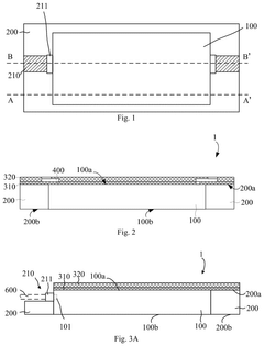
PatentInactiveSG185912A1
Innovation
- An alignment method involving multiple silicon waveguides arranged in parallel with a light source, such as a laser diode, to enhance alignment tolerance and coupling efficiency by using a combiner to combine light from multiple waveguides into an optical fiber.
Life Cycle Assessment of Silicon Photonics Products
Life Cycle Assessment (LCA) of silicon photonics products provides a comprehensive framework for evaluating environmental impacts throughout the entire product lifecycle. This assessment begins with raw material extraction, where silicon and rare earth elements are sourced, continuing through manufacturing processes that involve energy-intensive cleanroom operations and specialized fabrication techniques.
The manufacturing phase represents a significant environmental hotspot in silicon photonics, requiring substantial energy consumption, ultra-pure water usage, and specialized chemicals. These processes generate greenhouse gas emissions, particularly from the high energy demands of precision equipment and cleanroom maintenance. Additionally, the use of perfluorinated compounds and other chemicals in etching processes contributes to potential environmental hazards.
During the use phase, silicon photonics products generally demonstrate environmental advantages through reduced energy consumption compared to conventional electronic components. The integration of optical and electronic functions on a single chip significantly decreases power requirements for data transmission, potentially offsetting initial manufacturing impacts over the product lifetime.
End-of-life considerations present unique challenges due to the composite nature of silicon photonics packages. The integration of various materials—including silicon, metals, polymers, and sometimes rare earth elements—complicates recycling efforts. Current recycling technologies often struggle to efficiently separate these components, resulting in material loss and diminished recovery rates.
Recent LCA studies have quantified the carbon footprint of silicon photonics transceivers, revealing that manufacturing accounts for approximately 70-80% of lifecycle emissions, while use-phase energy consumption contributes the remaining portion. These assessments highlight opportunities for environmental optimization through design modifications, material substitutions, and manufacturing process improvements.
Comparative analyses between silicon photonics and traditional electronic components demonstrate significant environmental advantages, particularly in applications requiring high bandwidth and data transmission rates. The reduced energy consumption during operation can result in 30-50% lower lifetime carbon emissions for data center applications, despite potentially higher manufacturing impacts.
As environmental standards become increasingly stringent, LCA methodologies are evolving to incorporate more comprehensive impact categories beyond carbon emissions, including water footprint, resource depletion, and toxicity metrics. These expanded assessments provide a more holistic understanding of environmental performance and guide sustainable development in the silicon photonics industry.
Supply Chain Sustainability Considerations
The silicon photonics industry faces increasing pressure to align with global sustainability standards throughout its supply chain. Environmental regulations such as the EU's Restriction of Hazardous Substances (RoHS) and Registration, Evaluation, Authorization and Restriction of Chemicals (REACH) directly impact material selection for silicon photonics packaging. These standards restrict the use of lead-based solders and certain flame retardants, compelling manufacturers to develop alternative materials that maintain performance while meeting compliance requirements.
Carbon footprint considerations have become paramount in supply chain management for silicon photonics. The energy-intensive manufacturing processes, particularly in clean room environments, contribute significantly to the industry's environmental impact. Leading companies are implementing carbon accounting systems to track emissions across their supply chains, with some establishing science-based targets for reduction. This trend is accelerated by customer demands for environmentally responsible products and investor pressure for ESG (Environmental, Social, and Governance) compliance.
Water usage represents another critical sustainability factor, as semiconductor fabrication typically requires ultra-pure water in substantial quantities. In regions facing water scarcity, silicon photonics manufacturers must implement advanced water recycling systems and optimize processes to reduce consumption. Companies are increasingly adopting circular economy principles, designing packaging solutions that facilitate end-of-life recycling and minimize waste.
Supply chain transparency has emerged as a key requirement, with regulations like the EU's Corporate Sustainability Reporting Directive mandating detailed disclosure of environmental impacts. This drives the adoption of blockchain and other traceability technologies to verify sustainability claims throughout the supply chain. Suppliers are increasingly evaluated not only on cost and quality metrics but also on their environmental performance and compliance with standards.
The geographical distribution of the silicon photonics supply chain presents additional sustainability challenges. Components often travel globally before final assembly, creating a substantial carbon footprint from transportation. This has accelerated the trend toward regional manufacturing hubs and localized supply chains to reduce emissions and improve resilience against disruptions. Some companies are implementing supplier development programs to enhance environmental performance across their network.
Packaging innovation is increasingly driven by sustainability considerations, with research focused on biodegradable or recyclable materials that can meet the stringent performance requirements of photonic components. Advanced thermal management solutions that reduce energy consumption during operation are becoming competitive differentiators in the market, as customers factor lifetime environmental impact into purchasing decisions.
Unlock deeper insights with PatSnap Eureka Quick Research — get a full tech report to explore trends and direct your research. Try now!
Generate Your Research Report Instantly with AI Agent
Supercharge your innovation with PatSnap Eureka AI Agent Platform!