How Do Patents Shape the Future of Silicon Photonics Packaging
SEP 29, 20259 MIN READ
Generate Your Research Report Instantly with AI Agent
Patsnap Eureka helps you evaluate technical feasibility & market potential.
Silicon Photonics Packaging Patent Landscape and Objectives
Silicon photonics packaging has evolved significantly over the past two decades, transitioning from experimental laboratory concepts to commercial deployment in data centers. This evolution has been shaped substantially by patent activities that protect key innovations while simultaneously defining technological trajectories. The patent landscape in silicon photonics packaging reveals a complex interplay between technical advancement, market forces, and strategic positioning by industry leaders.
The historical development of silicon photonics packaging patents shows three distinct phases: foundational patents (2000-2010) establishing basic coupling and assembly techniques; optimization patents (2010-2018) focusing on manufacturing scalability and performance enhancement; and integration patents (2018-present) addressing heterogeneous integration challenges and system-level packaging solutions.
Current patent trends indicate increasing focus on wafer-level packaging techniques, optical I/O standardization, and thermal management solutions specific to photonic integrated circuits. These patents aim to address the fundamental challenges of coupling efficiency, alignment precision, and cost-effective manufacturing at scale - all critical barriers to widespread adoption of silicon photonics technology.
Geographically, patent filings demonstrate concentration in North America, East Asia, and Western Europe, with the United States maintaining leadership in fundamental innovation while Asian entities increasingly dominate manufacturing-oriented patents. This distribution reflects the global supply chain dynamics and regional specialization in the semiconductor and photonics industries.
The technical objectives revealed through patent analysis include achieving sub-micron alignment precision in high-volume manufacturing environments, developing hermetic sealing techniques compatible with optical interfaces, and creating packaging architectures that accommodate both electrical and optical interconnects while maintaining signal integrity across diverse operating conditions.
Patent citation networks highlight the emergence of several key technology clusters, including flip-chip bonding adaptations for photonic applications, polymer waveguide coupling interfaces, and automated active alignment systems. These clusters represent critical innovation pathways that will likely define future development trajectories.
The patent landscape also reveals strategic positioning by industry players, with telecommunications equipment manufacturers, semiconductor foundries, and specialized photonics companies establishing distinct patent portfolios that reflect their market positions and technical capabilities. Cross-licensing agreements and patent acquisitions further illustrate the strategic importance of packaging technologies in the broader silicon photonics ecosystem.
Market Demand Analysis for Advanced Photonic Integration
The global market for advanced photonic integration is experiencing unprecedented growth, driven by the increasing demand for high-speed data transmission, cloud computing, and artificial intelligence applications. Silicon photonics packaging, as a critical component of this ecosystem, represents a significant market opportunity with projections indicating a compound annual growth rate exceeding 20% through 2030. This growth trajectory is primarily fueled by data center operators seeking energy-efficient solutions to manage exponential increases in data traffic.
Telecommunications infrastructure represents the largest current market segment, with carriers worldwide upgrading networks to support 5G and eventually 6G technologies. These advanced networks require integrated photonic solutions capable of handling massive data throughput while maintaining signal integrity across long distances. The demand for silicon photonics packaging in this sector is particularly strong in North America, Europe, and developed Asian markets.
Data centers constitute the fastest-growing market segment, with hyperscale providers actively seeking solutions to address power consumption challenges. Silicon photonics offers significant advantages in reducing energy usage while increasing data transmission speeds. Market research indicates that approximately 40% of data center operators consider photonic integration a strategic priority for their infrastructure roadmaps, creating substantial demand for advanced packaging solutions.
Consumer electronics represents an emerging market with significant potential. As augmented reality, virtual reality, and autonomous vehicles gain mainstream adoption, the need for compact, energy-efficient photonic components increases dramatically. This segment is expected to generate substantial demand for miniaturized silicon photonic packages that can be integrated into portable and wearable devices.
Industrial automation and sensing applications constitute another growth vector, with manufacturing facilities increasingly deploying photonic sensors for precision monitoring and control. The industrial Internet of Things (IoT) ecosystem particularly benefits from silicon photonics' ability to provide high-bandwidth connections in electromagnetically noisy environments.
Market analysis reveals regional variations in demand patterns. Asia-Pacific leads in manufacturing capacity but North America dominates in terms of technology innovation and patent generation. European markets show particular strength in specialized applications for automotive and industrial sectors.
The market landscape is further shaped by evolving customer requirements, with end-users increasingly demanding standardized interfaces, reduced form factors, and improved thermal management. These requirements directly influence packaging technology development priorities and patent strategies across the industry.
Current Challenges in Silicon Photonics Packaging Technologies
Silicon photonics packaging faces significant technical challenges that impede its widespread commercial adoption. The integration of optical and electrical components at the package level remains one of the most formidable obstacles. Current packaging solutions struggle with achieving precise optical alignment between silicon photonic chips and optical fibers, with tolerances often required in the sub-micron range. This alignment challenge is exacerbated by thermal expansion mismatches between different materials used in the package, causing performance degradation over time and temperature variations.
Hermetic sealing represents another critical challenge, as photonic components are highly sensitive to environmental factors such as moisture and contaminants. Traditional electronic packaging methods often prove inadequate for maintaining the optical integrity required in silicon photonics applications. The industry currently lacks standardized packaging solutions, resulting in custom approaches that drive up costs and limit scalability.
Cost-effective manufacturing presents a persistent hurdle. While silicon photonics leverages CMOS fabrication infrastructure for chip production, packaging processes remain largely manual and difficult to automate. This creates a significant bottleneck in the manufacturing pipeline, with packaging costs often exceeding 80% of the total device cost. The absence of high-volume, automated packaging solutions severely restricts market penetration across various application domains.
Power consumption during operation constitutes another significant challenge. Current packaging technologies struggle to efficiently dissipate heat generated by active photonic components, leading to thermal management issues that affect device performance and reliability. This is particularly problematic in data center applications where energy efficiency is paramount.
Testing and quality assurance of packaged silicon photonic devices present unique difficulties. Unlike electronic components, optical testing requires specialized equipment and procedures that are not easily integrated into standard manufacturing flows. The lack of standardized testing methodologies increases production costs and time-to-market.
Coupling efficiency between optical fibers and silicon waveguides remains suboptimal in many packaging solutions, resulting in significant signal losses. Current approaches using grating couplers or edge couplers each have limitations in bandwidth, polarization sensitivity, or manufacturing complexity that compromise overall system performance.
Patent analysis reveals that while significant innovation is occurring in addressing these challenges, many solutions remain proprietary and fragmented across different industry players. This fragmentation hinders the development of universal standards and interoperable solutions that could accelerate market adoption and reduce costs through economies of scale.
Current Patent-Protected Packaging Solutions
01 Optical coupling techniques in silicon photonics packaging
Various optical coupling techniques are employed in silicon photonics packaging to efficiently transfer light between optical components. These include edge coupling, grating coupling, and evanescent coupling methods that optimize the interface between photonic chips and optical fibers. Advanced coupling designs minimize insertion loss and enhance alignment tolerance, which is critical for maintaining signal integrity in photonic integrated circuits.- Optical coupling techniques in silicon photonics packaging: Various optical coupling techniques are employed in silicon photonics packaging to efficiently transfer light between optical components. These include edge coupling, grating couplers, and evanescent coupling methods that minimize insertion loss. Advanced alignment techniques ensure precise positioning of optical components to maintain signal integrity across interfaces. These coupling solutions address the challenges of mode mismatch and polarization sensitivity in photonic integrated circuits.
- Thermal management solutions for silicon photonics: Thermal management is critical in silicon photonics packaging due to temperature sensitivity of optical components. Various approaches include integration of thermal vias, heat spreaders, and thermoelectric coolers to dissipate heat efficiently. Advanced thermal interface materials improve heat transfer between components. Temperature control systems maintain stable operating conditions for wavelength-sensitive devices, ensuring consistent performance across varying environmental conditions.
- Hermetic sealing and protection techniques: Hermetic sealing technologies protect sensitive photonic components from environmental factors such as moisture, dust, and contaminants. Various approaches include glass lid bonding, metal sealing, and polymer encapsulation. These techniques maintain optical alignment while providing mechanical protection. Advanced materials with matched coefficients of thermal expansion minimize stress on optical components during temperature fluctuations, ensuring long-term reliability and stable optical performance.
- Integration with electronic components: Silicon photonics packaging involves integration of optical and electronic components to create complete optoelectronic systems. Approaches include 2.5D and 3D integration techniques, through-silicon vias, and interposer technologies. Co-packaging of photonic integrated circuits with electronic integrated circuits addresses signal integrity challenges at high data rates. These integration methods enable compact form factors while maintaining high-speed communication between optical and electronic domains.
- Wafer-level packaging techniques: Wafer-level packaging techniques for silicon photonics enable cost-effective mass production while maintaining optical performance. These include wafer bonding, through-silicon vias for vertical integration, and collective alignment methods. Wafer-level testing capabilities allow for early detection of defects before final assembly. Advanced materials and processes ensure compatibility with standard semiconductor manufacturing flows while addressing the unique requirements of optical components.
02 Thermal management solutions for photonic packages
Thermal management is crucial in silicon photonics packaging to maintain operational stability and reliability. Solutions include integrated heat sinks, thermal interface materials, and active cooling systems that efficiently dissipate heat generated during operation. These thermal management approaches prevent wavelength drift and performance degradation in temperature-sensitive photonic components, ensuring consistent operation across varying environmental conditions.Expand Specific Solutions03 Hermetic sealing and protection techniques
Hermetic sealing and protection methods are essential for silicon photonics packages to shield sensitive optical components from environmental factors. Techniques include glass lid bonding, metal sealing, and polymer encapsulation that provide moisture resistance and mechanical protection. These approaches extend device lifetime by preventing contamination and physical damage while maintaining optical transparency where required for light transmission.Expand Specific Solutions04 Integration of electronic and photonic components
The integration of electronic and photonic components in a single package presents unique challenges and solutions in silicon photonics. Approaches include 2.5D and 3D integration techniques, interposer technologies, and hybrid bonding methods that enable efficient communication between electronic and photonic domains. These integration strategies minimize signal latency, reduce power consumption, and enhance overall system performance while addressing the different material requirements of each component type.Expand Specific Solutions05 Wafer-level packaging processes for mass production
Wafer-level packaging processes enable cost-effective mass production of silicon photonic devices. These include wafer bonding, through-silicon vias (TSVs), and collective assembly techniques that allow parallel processing of multiple devices. Such approaches significantly reduce manufacturing costs while maintaining high yield and reliability, making silicon photonics more commercially viable for widespread deployment in telecommunications, data centers, and sensing applications.Expand Specific Solutions
Key Industry Players and Patent Holders Analysis
Silicon photonics packaging is evolving through a competitive landscape characterized by early commercial maturity and rapid growth. The market is projected to expand significantly as data centers and telecommunications demand higher bandwidth solutions. Intel leads with extensive patent portfolios focusing on integration techniques, while TSMC and GlobalFoundries leverage their semiconductor manufacturing expertise to develop advanced packaging solutions. Ayar Labs and Xscape Photonics represent innovative startups disrupting traditional approaches with novel co-packaging technologies. Huawei and IBM are investing heavily in patents related to optical interconnect solutions. The technology is transitioning from research to commercial deployment, with companies like Mellanox (NVIDIA) and Cisco developing standards-based approaches to ensure interoperability across the ecosystem.
Intel Corp.
Technical Solution: Intel has pioneered advanced silicon photonics packaging technologies through their integrated approach combining photonics with CMOS electronics. Their patented technologies focus on heterogeneous integration methods that allow optical components to be directly integrated with electronic circuits on the same silicon substrate. Intel's Silicon Photonics platform utilizes wafer-scale manufacturing processes to create high-volume, low-cost optical interconnects. Their patents cover critical areas including waveguide coupling structures, optical I/O solutions, and thermal management techniques specific to photonic integrated circuits. Intel has developed innovative flip-chip bonding methods for integrating III-V lasers with silicon waveguides, addressing one of the fundamental challenges in silicon photonics. Their packaging solutions enable data transmission rates exceeding 400 Gbps per fiber with plans to scale to terabit speeds in future iterations. Intel's patent portfolio also includes novel approaches to fiber attachment technologies and hermetic sealing methods critical for maintaining long-term reliability of photonic components.
Strengths: Intel's vertical integration capabilities allow them to optimize both chip design and packaging technologies simultaneously. Their established semiconductor manufacturing infrastructure provides economies of scale for photonics production. Weaknesses: Their proprietary packaging approaches may limit ecosystem development compared to more open standards, and their solutions tend to be optimized for data center applications rather than broader markets.
Taiwan Semiconductor Manufacturing Co., Ltd.
Technical Solution: TSMC has developed extensive patent portfolios around silicon photonics packaging that leverage their advanced semiconductor manufacturing capabilities. Their approach focuses on monolithic and hybrid integration techniques that enable high-density photonic-electronic integration. TSMC's patents cover specialized through-silicon via (TSV) technologies adapted specifically for photonic applications, allowing vertical integration of optical components with electronic drivers. They've pioneered low-loss optical coupling methods between different material platforms and waveguide structures. TSMC's packaging solutions address thermal isolation challenges between photonic and electronic components, which is critical for maintaining wavelength stability in dense wavelength division multiplexing (DWDM) applications. Their patents also cover novel approaches to optical alignment during the packaging process, utilizing passive alignment structures that can achieve sub-micron precision at wafer scale. TSMC has developed specialized materials and processes for optical interface protection during packaging, ensuring long-term reliability even in harsh environmental conditions. Their integrated photonics packaging technologies support applications ranging from high-performance computing interconnects to next-generation 5G/6G optical transceivers.
Strengths: TSMC's unparalleled semiconductor manufacturing expertise allows for extremely precise and repeatable photonic component fabrication. Their established ecosystem of partners enables rapid commercialization pathways. Weaknesses: As primarily a foundry, TSMC may lack the end-to-end system knowledge that vertically integrated companies possess, potentially limiting optimization across the full photonic system stack.
Critical Patent Analysis and Technical Innovations
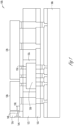
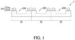
Semiconductor assembly with waveguide and glass substrate
PatentPendingEP4191307A1
Innovation
- The use of laser-based technology for integrating photonic integrated circuits, electronic integrated circuits, and substrates with low-loss coupling, including laser-made glass-to-glass bonds and embedded waveguides formed through laser direct writing, addresses these challenges by minimizing coupling loss and enabling high-voltage compatibility.
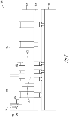
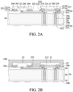
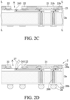
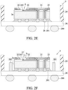
Electronic package and manufacturing method thereof
PatentActiveUS20230420391A1
Innovation
- The design of a photonic die with conductive vias, an electronic element, and a functional part with a hollow area, where the electronic element is electrically connected to the conductive vias and the functional part is bonded with dummy bumps, allowing for direct signal transmission to an optical fiber through a cladding layer, thereby shortening the signal transmission path.
Standards and Interoperability Considerations
The standardization landscape for silicon photonics packaging is evolving rapidly as the technology matures, with patents playing a crucial role in shaping industry standards. Major standardization bodies including IEEE, IEC, and the Optical Internetworking Forum (OIF) have established working groups specifically focused on silicon photonics interconnects and packaging technologies. These efforts aim to create unified specifications for optical interfaces, thermal management protocols, and testing methodologies that enable interoperability across different manufacturers' components.
Patent portfolios from industry leaders like Intel, IBM, and Cisco are significantly influencing these emerging standards. Companies with extensive patent holdings in key packaging technologies—such as optical coupling techniques, hermetic sealing methods, and thermal management solutions—often secure positions on standards committees, allowing them to steer specifications in directions aligned with their intellectual property. This creates a complex ecosystem where standards development and patent strategy are increasingly intertwined.
Interoperability remains a critical challenge in silicon photonics packaging, with patents both enabling and potentially hindering progress. Cross-licensing agreements between major players have become essential to ensure that standardized interfaces can be implemented without infringement concerns. The Co-Packaged Optics Collaboration and the Consortium for On-Board Optics represent industry efforts to develop open specifications that balance proprietary innovation with necessary interoperability.
Patent analysis reveals emerging trends toward modular packaging approaches that allow for mix-and-match integration of components from different vendors. These approaches require standardized electrical and optical interfaces, with patents covering specific implementation techniques rather than the interface definitions themselves. This distinction is crucial for maintaining an open ecosystem while protecting proprietary manufacturing methods.
The geographical distribution of standards-related patents shows interesting patterns, with North American companies focusing on system-level integration patents, while Asian manufacturers hold significant IP in manufacturing processes and assembly techniques. European entities often focus on testing and qualification methodologies. This distribution creates natural collaboration opportunities but also potential friction points in global standards adoption.
Looking forward, patents covering software-defined optical interfaces and automated testing protocols are likely to become increasingly valuable as the industry moves toward more flexible, programmable photonic systems. These patents will shape how silicon photonics components interact with broader data center and telecommunications infrastructure, potentially defining competitive advantages for decades to come.
IP Strategy and Competitive Positioning
In the competitive landscape of silicon photonics packaging, intellectual property (IP) has emerged as a critical strategic asset that shapes market dynamics and technological advancement. Companies with robust patent portfolios in this domain can secure significant competitive advantages through licensing agreements, cross-licensing opportunities, and freedom-to-operate positions. The strategic value of patents extends beyond mere legal protection, serving as bargaining chips in negotiations and indicators of technological leadership.
Leading organizations in silicon photonics packaging have adopted diverse IP strategies. Some focus on building broad patent portfolios covering fundamental packaging techniques, while others target specific high-value applications or niche solutions. This strategic differentiation has created a complex competitive ecosystem where patent position often determines market access and partnership opportunities.
Patent analysis reveals distinct geographical patterns in IP development. North American companies typically emphasize innovation in optical coupling and thermal management solutions, while Asian entities demonstrate strength in manufacturing processes and materials science applications. European organizations often focus on specialized integration techniques and testing methodologies. These regional specializations create opportunities for strategic collaborations across borders.
The evolution of patent filing trends indicates a shift from broad conceptual patents toward highly specific implementation techniques. Early patents in silicon photonics packaging focused on fundamental approaches, while recent filings increasingly address practical manufacturing challenges, reliability issues, and cost reduction methods. This progression reflects the technology's maturation and commercialization trajectory.
For new market entrants, navigating the patent landscape requires careful strategic planning. Options include developing non-infringing alternative technologies, pursuing licensing agreements with patent holders, or identifying white space opportunities where innovation remains relatively unconstrained by existing IP. The choice depends on available resources, time-to-market requirements, and long-term business objectives.
Patent quality has become increasingly important as the technology matures. While patent quantity previously dominated strategic considerations, the industry now recognizes that fewer high-quality patents covering critical technological bottlenecks often provide greater competitive advantage than numerous peripheral patents. This shift has implications for R&D investment decisions and IP portfolio management approaches.
Looking forward, companies that strategically align their IP portfolios with emerging market needs will likely secure advantageous positions in the evolving silicon photonics ecosystem. The most successful organizations will balance defensive patenting strategies with offensive approaches that create barriers to competition while enabling strategic partnerships.
Unlock deeper insights with Patsnap Eureka Quick Research — get a full tech report to explore trends and direct your research. Try now!
Generate Your Research Report Instantly with AI Agent
Supercharge your innovation with Patsnap Eureka AI Agent Platform!