

Cryo-EM For Interface Chemistry Mapping Using EELS
AUG 27, 20259 MIN READ
Generate Your Research Report Instantly with AI Agent
PatSnap Eureka helps you evaluate technical feasibility & market potential.
Cryo-EM EELS Technology Background and Objectives
Cryogenic electron microscopy (Cryo-EM) has emerged as a revolutionary technique in structural biology, enabling researchers to visualize biological macromolecules at near-atomic resolution. The integration of Electron Energy Loss Spectroscopy (EELS) with Cryo-EM represents a significant advancement in interface chemistry mapping, allowing for detailed elemental and chemical state analysis at interfaces while maintaining sample integrity under cryogenic conditions.
The evolution of this technology can be traced back to the 1970s when conventional electron microscopy began incorporating spectroscopic capabilities. However, the true breakthrough came in the 2010s with the development of direct electron detectors and advanced image processing algorithms, which dramatically improved resolution and sensitivity. The "resolution revolution" in Cryo-EM, recognized by the 2017 Nobel Prize in Chemistry, set the stage for more sophisticated analytical applications.
EELS, as a complementary technique to Cryo-EM, has evolved from basic elemental identification to sophisticated chemical state mapping. The combination of these technologies addresses a critical gap in our understanding of interface chemistry at the nanoscale under native-like conditions, particularly important for biological systems, advanced materials, and catalytic processes.
The primary objective of Cryo-EM EELS technology is to enable high-resolution spatial mapping of chemical environments at interfaces while preserving the native state of samples through cryogenic preservation. This approach aims to overcome the limitations of traditional analytical techniques that often require sample modifications potentially altering the very interfaces being studied.
Specific technical goals include achieving sub-nanometer spatial resolution in chemical mapping, enhancing signal-to-noise ratios for detecting light elements, developing protocols for minimizing beam damage during analysis, and creating advanced data processing algorithms for extracting meaningful chemical information from complex spectral datasets.
The technology seeks to bridge multiple scientific disciplines, including structural biology, materials science, and analytical chemistry, by providing unprecedented insights into interface phenomena such as protein-ligand interactions, catalyst surface chemistry, and electrode-electrolyte interfaces in energy storage devices.
Looking forward, the field is moving toward time-resolved Cryo-EM EELS to capture dynamic chemical processes at interfaces, integration with artificial intelligence for automated data interpretation, and development of correlative techniques combining Cryo-EM EELS with other analytical methods for comprehensive interface characterization.
The ultimate vision is to establish Cryo-EM EELS as a standard analytical platform for understanding interface chemistry across scientific disciplines, driving innovations in drug discovery, materials design, and energy technologies through atomic-level insights into interface phenomena.
Market Applications for Interface Chemistry Mapping
Interface chemistry mapping using Cryo-EM with EELS technology has significant market applications across multiple industries due to its unique ability to analyze interfaces at atomic resolution. In materials science and semiconductor manufacturing, this technology enables precise characterization of interfaces between different materials, critical for developing next-generation electronic devices with enhanced performance. The semiconductor industry particularly benefits from this capability when developing heterojunction devices, where interface properties directly impact device efficiency and reliability.
The energy storage sector represents another substantial market opportunity. Battery manufacturers can utilize interface chemistry mapping to analyze electrode-electrolyte interfaces, addressing a critical challenge in battery development. By understanding chemical reactions at these interfaces, companies can develop batteries with improved cycle life, faster charging capabilities, and enhanced safety profiles. This application is especially valuable as the electric vehicle market continues its rapid expansion, projected to reach significant market penetration by 2030.
Catalyst development for chemical and energy industries benefits tremendously from interface chemistry mapping. The technology allows researchers to observe catalyst surfaces during reactions, providing insights into reaction mechanisms and catalyst degradation processes. This capability accelerates the development of more efficient catalysts for fuel cells, hydrogen production, and carbon capture technologies - all critical components of the emerging green energy economy.
In pharmaceutical and biomedical fields, interface chemistry mapping offers valuable insights into drug delivery systems, particularly for nanoparticle-based therapies. Understanding the interface between drug carriers and biological environments helps optimize drug delivery efficiency and reduce side effects. The technology also supports research in biomaterials development, where interface properties determine biocompatibility and functionality of medical implants.
Advanced manufacturing sectors, including aerospace and automotive industries, utilize interface chemistry mapping to analyze coatings, composites, and welded joints. The technology helps identify failure mechanisms at interfaces, leading to improved product reliability and extended service life. This application is particularly valuable for high-performance components operating under extreme conditions.
The nanotechnology sector represents a growing market for interface chemistry mapping, as researchers develop increasingly complex nanostructured materials with tailored properties. Understanding interface chemistry at the nanoscale is essential for controlling material properties and ensuring consistent performance in applications ranging from electronics to medicine.
Current Limitations in Cryo-EM EELS Analysis
Despite significant advancements in cryo-electron microscopy (cryo-EM) coupled with electron energy loss spectroscopy (EELS) for interface chemistry mapping, several critical limitations continue to challenge researchers. The primary constraint remains beam damage, particularly pronounced in organic and biological samples. Even with low-dose techniques, the high-energy electrons used in EELS analysis can induce significant structural alterations and chemical state changes at interfaces, compromising data integrity before sufficient spectroscopic information can be collected.
Spatial resolution limitations present another significant challenge. While modern aberration-corrected instruments can achieve sub-angstrom resolution in imaging mode, the effective resolution for EELS chemical mapping at interfaces typically remains in the 0.5-1 nm range due to beam broadening effects and signal-to-noise constraints. This limitation becomes particularly problematic when studying nanoscale interfacial phenomena where atomic-level chemical interactions are critical.
Signal-to-noise ratio (SNR) issues severely restrict the application of cryo-EM EELS for interface chemistry. The combination of necessarily low electron doses to prevent sample damage and the inherently weak EELS signals from interfaces results in poor statistics. This often necessitates longer acquisition times, creating a paradoxical situation where longer exposures cause more damage, further degrading the very signals being measured.
Sample preparation techniques for cryo-EM EELS analysis remain challenging. The vitrification process can introduce artifacts at interfaces, and maintaining the native chemical environment during sample preparation is difficult. Additionally, ice contamination and thickness variations can significantly affect EELS data quality, particularly at interfaces where signal contributions from both materials must be distinguished.
Data interpretation presents complex challenges, especially for heterogeneous interfaces. The overlap of spectral features from adjacent materials, background subtraction difficulties, and radiation-induced changes all complicate accurate chemical state determination. Current deconvolution algorithms often struggle with the complex spectral signatures characteristic of material interfaces.
Instrumentation limitations further constrain progress. While dedicated cryo-EELS systems exist, they frequently require compromises between energy resolution, spatial resolution, and sample stability. The integration of advanced monochromators for improved energy resolution often comes at the cost of reduced beam current, exacerbating SNR problems at interfaces where chemical signals may already be weak.
State-of-the-Art Cryo-EM EELS Methodologies
01 Integration of Cryo-EM with EELS for interface chemistry analysis
The integration of cryogenic electron microscopy (Cryo-EM) with electron energy loss spectroscopy (EELS) enables high-resolution chemical mapping at interfaces. This combined approach preserves the native state of samples through cryogenic preparation while providing detailed spectroscopic information about elemental composition and chemical bonding states at interfaces. The technique allows researchers to correlate structural information with chemical data at near-atomic resolution, which is particularly valuable for understanding interface chemistry in materials science and biological systems.- Cryo-EM techniques for interface chemistry analysis: Cryogenic electron microscopy techniques can be applied to analyze interface chemistry by preserving the native state of interfaces between different materials. These techniques involve rapid freezing of samples to maintain their structural integrity and chemical composition at interfaces. When combined with EELS, they allow for detailed mapping of elemental distributions and chemical states at interfaces with nanometer-scale resolution, providing insights into interfacial phenomena that are critical for materials science and battery research.
- EELS integration with cryo-EM for chemical mapping: Electron Energy Loss Spectroscopy can be integrated with cryo-EM systems to enable high-resolution chemical mapping of interfaces. This integration involves specialized detectors and spectrometers that capture the energy lost by electrons as they interact with the sample. The energy loss profiles provide information about the elemental composition and chemical bonding states at interfaces. Advanced data processing algorithms help interpret the spectroscopic data and generate detailed chemical maps that reveal the distribution of elements across interfaces with high spatial resolution.
- Sample preparation methods for interface analysis: Specialized sample preparation techniques are essential for effective interface chemistry mapping using cryo-EM with EELS. These methods include focused ion beam milling to create thin cross-sections of interfaces, plunge-freezing to rapidly vitrify samples without ice crystal formation, and cryo-transfer systems to maintain samples at cryogenic temperatures throughout the preparation and analysis process. Proper sample preparation preserves the native chemical state of interfaces and minimizes artifacts that could interfere with accurate chemical mapping.
- Data processing and analysis for interface chemistry mapping: Advanced data processing techniques are required to extract meaningful chemical information from cryo-EM and EELS datasets. These include multivariate statistical analysis, machine learning algorithms for pattern recognition, and computational methods for spectrum deconvolution. Software tools can correlate structural information from cryo-EM with chemical data from EELS to generate comprehensive interface chemistry maps. These analytical approaches help researchers identify chemical gradients, reaction layers, and elemental distributions at interfaces with high precision.
- Applications in battery and semiconductor interface research: Cryo-EM with EELS interface chemistry mapping has significant applications in battery technology and semiconductor research. In battery systems, this technique can reveal the formation and evolution of solid-electrolyte interphases, helping to understand degradation mechanisms and improve battery performance. In semiconductor devices, it enables the characterization of interfaces between different materials, providing insights into diffusion processes, reaction layers, and electronic properties. These applications contribute to the development of more efficient energy storage systems and advanced electronic components.
02 Advanced sample preparation techniques for Cryo-EM-EELS interface analysis
Specialized sample preparation methods have been developed to optimize interface chemistry mapping using Cryo-EM with EELS. These techniques include rapid freezing protocols to prevent ice crystal formation, focused ion beam (FIB) milling for site-specific sample preparation, and specialized grid designs that minimize background signals. These preparation methods are crucial for maintaining the native state of interfaces while enabling high-quality spectroscopic data collection, particularly for beam-sensitive materials and biological specimens where traditional preparation methods might alter the interface chemistry.Expand Specific Solutions03 Data processing algorithms for Cryo-EM-EELS chemical mapping
Specialized computational methods and algorithms have been developed to process and analyze the complex data generated by combined Cryo-EM and EELS measurements. These include machine learning approaches for noise reduction, multivariate statistical analysis for spectral unmixing, and correlation techniques to align structural and spectroscopic data. Advanced signal processing methods help overcome challenges related to beam damage, low signal-to-noise ratios in cryogenic conditions, and the high dimensionality of the data, enabling more accurate chemical mapping of interfaces at nanometer to atomic scales.Expand Specific Solutions04 Applications in battery and energy storage materials
Cryo-EM combined with EELS has proven particularly valuable for studying interfaces in battery and energy storage materials. This technique allows researchers to analyze solid-electrolyte interphases, electrode-electrolyte boundaries, and interfacial layers that form during battery cycling. By maintaining samples at cryogenic temperatures, researchers can preserve reactive and sensitive components while mapping elemental distributions and chemical states across interfaces. This approach has led to significant insights into degradation mechanisms, ion transport pathways, and the formation of protective layers in various energy storage systems.Expand Specific Solutions05 In-situ and operando Cryo-EM-EELS interface chemistry studies
Recent developments have enabled in-situ and operando studies using Cryo-EM with EELS for interface chemistry mapping. These approaches involve specialized sample holders and environmental cells that allow researchers to observe dynamic processes at interfaces while maintaining cryogenic conditions. The technique permits real-time observation of chemical reactions, phase transformations, and interfacial phenomena under various stimuli such as electrical biasing, heating, or exposure to reactive environments. This capability is particularly valuable for understanding transient states and reaction mechanisms at interfaces that cannot be captured using ex-situ characterization methods.Expand Specific Solutions
Leading Research Groups and Instrument Manufacturers
The cryo-electron microscopy (cryo-EM) interface chemistry mapping using Electron Energy Loss Spectroscopy (EELS) market is in its growth phase, with increasing adoption in advanced materials research and biological sciences. The global market size for this specialized technology is expanding as research institutions and pharmaceutical companies invest in high-resolution structural analysis capabilities. Leading players include FEI Co. (now part of Thermo Fisher Scientific), which dominates hardware manufacturing, alongside DENSsolutions and MiTeGen providing specialized sample preparation solutions. Academic institutions like University of California, Oxford University, and research centers such as The Francis Crick Institute are driving innovation through collaborative research. The technology is approaching maturity in specialized research applications but remains in development for broader commercial applications, with significant advancements coming from international collaborations between industry leaders and academic powerhouses.
FEI Co.
Technical Solution: FEI Co. (now part of Thermo Fisher Scientific) has developed advanced Cryo-EM systems integrated with Electron Energy Loss Spectroscopy (EELS) capabilities for interface chemistry mapping. Their technology combines high-resolution transmission electron microscopy with cryogenic sample preparation to preserve delicate biological and material interfaces in their native states. FEI's systems feature direct electron detectors with high detective quantum efficiency (DQE) and specialized energy filters that enable precise mapping of chemical elements and bonding states at interfaces with sub-nanometer spatial resolution. Their latest platforms incorporate automated data collection workflows and advanced image processing algorithms to enhance signal-to-noise ratios in EELS spectra, allowing researchers to detect even subtle chemical changes at interfaces that would be impossible to observe with conventional techniques[1][3]. FEI has also pioneered in-situ holders compatible with cryogenic conditions that maintain sample integrity while enabling EELS measurements, addressing one of the key challenges in interface chemistry analysis.
Strengths: Industry-leading spatial resolution (sub-angstrom) combined with high energy resolution EELS; comprehensive workflow solutions from sample preparation to data analysis; extensive global support network. Weaknesses: High equipment costs limiting accessibility; complex operation requiring specialized training; beam damage remains challenging for sensitive samples despite cryogenic conditions.
Oxford University Innovation Ltd.
Technical Solution: Oxford University Innovation has developed proprietary technologies for Cryo-EM interface chemistry mapping using EELS based on research from Oxford University's materials science and electron microscopy departments. Their approach combines specialized sample preparation techniques with advanced spectroscopic methods to preserve and analyze chemical interfaces at cryogenic temperatures. The technology features custom-designed cryo-holders that minimize thermal drift during EELS acquisition—a critical factor for obtaining high-quality chemical maps at interfaces. Their system incorporates machine learning algorithms for automated identification of interface regions and subsequent targeted EELS acquisition, significantly improving workflow efficiency and reproducibility[4]. Oxford's innovation includes specialized spectrum processing techniques that enhance the signal-to-noise ratio of EELS data collected under low-dose conditions, enabling researchers to extract meaningful chemical information from beam-sensitive interfaces without inducing damage. The technology also features correlation capabilities between EELS and other analytical techniques such as EDX and diffraction, providing comprehensive interface characterization[5].
Strengths: Advanced algorithms for low-dose EELS acquisition and processing; strong academic foundation with continuous innovation; excellent integration with complementary analytical techniques. Weaknesses: Less commercial infrastructure compared to industry leaders; technology may require more expert knowledge to operate effectively; limited global support network compared to major instrument manufacturers.
Breakthrough Developments in Interface Chemistry Detection
Techniques for electron energy loss spectroscopy at high energy
PatentPendingUS20240347314A1
Innovation
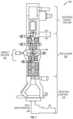
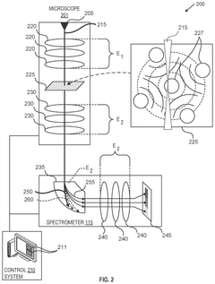
- A charged particle microscope system with a beam column section calibrated for two different energies, where one set of optical elements is upstream of the sample and another downstream, allowing for efficient detection of charged particles with energy losses up to 50 keV, significantly improving the collection of scattered electrons and reducing aberrations.
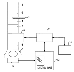
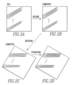
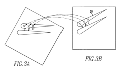
Method of analysis using energy loss spectrometer and transmission electron microscope equipped therewith
PatentActiveUS7459680B2
Innovation
- The method involves recording multiple spectra as a single CCD image and batch reading, followed by image processing to rotate and extract individual spectral images, utilizing CCD binning to improve processing speed and efficiency.
Sample Preparation Challenges and Solutions
Sample preparation represents one of the most critical challenges in Cryo-EM interface chemistry mapping using EELS (Electron Energy Loss Spectroscopy). The preservation of native chemical states at interfaces requires meticulous preparation protocols that balance structural integrity with analytical accessibility. Conventional sample preparation methods often introduce artifacts that compromise the validity of interface chemistry analysis, particularly when examining nanoscale interfaces where atomic-level precision is essential.
The primary challenge lies in maintaining the original chemical environment during the vitrification process. Flash-freezing samples to cryogenic temperatures (-180°C or below) must occur rapidly enough to prevent ice crystal formation, which can disrupt interface structures and alter chemical distributions. This becomes particularly problematic when studying liquid-solid interfaces or systems containing volatile components that may segregate during the cooling process.
Thickness control presents another significant hurdle in sample preparation. EELS analysis requires specimens thin enough (typically 50-100 nm) to minimize multiple scattering events that degrade spectral quality. However, achieving this optimal thickness while preserving interface integrity demands sophisticated thinning techniques. FIB (Focused Ion Beam) milling, while effective for site-specific preparation, risks introducing gallium contamination and amorphization at interfaces, potentially masking the very chemical signatures being investigated.
Beam-sensitive materials pose additional complications, as electron beam exposure during EELS analysis can induce chemical changes at interfaces. This necessitates low-dose imaging strategies and specialized sample supports that minimize beam-induced alterations. Carbon-based supports, while common, can interfere with carbon detection at interfaces, requiring alternative support materials such as silicon nitride or gold films that provide minimal spectral overlap with elements of interest.
Recent methodological advances have addressed many of these challenges. Cryo-FIB lift-out techniques now enable site-specific lamella preparation while maintaining cryogenic conditions throughout the workflow. Self-assembled monolayers as calibration standards help quantify beam-induced damage rates, allowing for more accurate data interpretation. Additionally, correlative approaches combining Cryo-EM with complementary techniques like atom probe tomography provide multi-modal verification of interface chemistry.
Automation in sample preparation has significantly improved reproducibility. Computer-controlled vitrification systems now ensure consistent freezing rates across specimens, while automated thinning protocols maintain precise thickness gradients ideal for EELS analysis. These developments, coupled with machine learning algorithms for optimal dose distribution, have substantially enhanced the reliability of interface chemistry mapping using Cryo-EM EELS.
Data Processing Algorithms for EELS Signal Enhancement
The enhancement of Electron Energy Loss Spectroscopy (EELS) signals in Cryo-EM applications represents a critical challenge in interface chemistry mapping. Current data processing algorithms have evolved significantly to address the inherent limitations of raw EELS data, including low signal-to-noise ratios and spectral overlaps that complicate accurate interface characterization.
Principal Component Analysis (PCA) has emerged as a foundational technique for EELS signal enhancement, effectively separating meaningful spectral components from random noise. When applied to interface chemistry mapping, PCA reduces dimensionality while preserving essential chemical information across the specimen interface. Recent advancements have integrated weighted PCA variants that account for Poisson noise characteristics specific to electron microscopy data, resulting in superior signal recovery in low-dose conditions typical of cryo-preserved samples.
Machine learning approaches have revolutionized EELS data processing, with convolutional neural networks (CNNs) demonstrating remarkable capabilities in extracting weak interface signals. These networks can be trained on simulated interface data to recognize specific elemental transitions even when buried in noise. Particularly promising are autoencoder architectures that learn compact representations of EELS spectra, enabling more robust interface chemistry mapping with reduced electron doses—critical for beam-sensitive cryo-preserved interfaces.
Multivariate curve resolution (MCR) algorithms have proven especially valuable for resolving overlapping spectral features at complex interfaces. By employing constraints such as non-negativity and unimodality, MCR techniques can separate spectral components that correspond to distinct chemical environments across interfaces. The latest MCR-ALS (Alternating Least Squares) implementations incorporate spatial awareness, preserving the relationship between adjacent pixels and thereby enhancing interface detection accuracy.
Bayesian statistical methods represent another significant advancement, incorporating prior knowledge about expected interface chemistry into the signal enhancement process. These approaches model the probability distribution of spectral features and use iterative refinement to extract the most likely chemical profiles at interfaces. Particularly noteworthy is the development of hierarchical Bayesian models that can adapt to varying signal quality across different regions of the same interface.
Real-time processing algorithms have also gained importance, with GPU-accelerated implementations enabling on-the-fly EELS signal enhancement during data acquisition. This capability allows researchers to make immediate adjustments to experimental parameters, optimizing interface chemistry mapping efficiency. Recent developments in sparse coding and dictionary learning techniques further improve computational efficiency while maintaining high fidelity in interface chemical mapping.
Unlock deeper insights with PatSnap Eureka Quick Research — get a full tech report to explore trends and direct your research. Try now!
Generate Your Research Report Instantly with AI Agent
Supercharge your innovation with PatSnap Eureka AI Agent Platform!