

Exploring PEEK Polymer's Role in MEMS Technology
OCT 24, 202510 MIN READ
Generate Your Research Report Instantly with AI Agent
PatSnap Eureka helps you evaluate technical feasibility & market potential.
PEEK Polymer in MEMS: Background and Objectives
Polyetheretherketone (PEEK) has emerged as a significant material in the evolution of Micro-Electro-Mechanical Systems (MEMS) technology over the past three decades. This high-performance thermoplastic polymer was first developed in the 1970s but gained prominence in advanced applications during the 1990s due to its exceptional mechanical, thermal, and chemical properties. The trajectory of PEEK in MEMS technology represents a shift from traditional silicon-based approaches toward more versatile polymer-based solutions that offer unique advantages in specific application domains.
The historical development of PEEK in MEMS can be traced through several key milestones. Initially, MEMS devices relied predominantly on silicon and other inorganic materials. However, as applications expanded into biomedical, aerospace, and harsh environment sensing, the limitations of these conventional materials became apparent. PEEK's introduction addressed critical challenges including biocompatibility, chemical resistance, and mechanical flexibility that silicon-based systems could not adequately provide.
Current technological trends indicate an accelerating integration of PEEK polymers in next-generation MEMS devices. This evolution is driven by increasing demands for miniaturization, functionality in extreme environments, and biocompatible interfaces. The polymer's glass transition temperature of approximately 143°C and melting point around 343°C enable operation in temperature ranges that exceed the capabilities of many other polymers, making it particularly valuable for harsh environment applications.
The primary technical objectives for PEEK in MEMS technology encompass several dimensions. First, researchers aim to optimize microfabrication techniques specifically tailored for PEEK, including precision injection molding, laser micromachining, and novel bonding methods that preserve the material's inherent properties. Second, there is significant focus on enhancing PEEK's surface properties through functionalization techniques to improve adhesion, wettability, and biocompatibility for specialized applications.
Another critical objective involves the development of PEEK composites that incorporate nanofillers such as carbon nanotubes, graphene, or ceramic particles to enhance specific properties like electrical conductivity, thermal management, or mechanical strength while maintaining processability. These composite materials potentially represent the next frontier in PEEK-based MEMS technology, enabling entirely new device architectures and functionalities.
The integration of PEEK with other materials in heterogeneous MEMS structures presents both opportunities and challenges. Current research aims to develop reliable interfaces between PEEK and metals, ceramics, or semiconductors to create truly multifunctional devices. This includes addressing thermal expansion mismatches, adhesion issues, and long-term reliability under operational stresses.
Market Analysis for PEEK-based MEMS Applications
The global market for PEEK-based MEMS applications is experiencing significant growth, driven by increasing demand for high-performance materials in harsh operating environments. Current market valuations indicate that the PEEK polymer market for microelectromechanical systems reached approximately 320 million USD in 2022, with projections suggesting a compound annual growth rate of 7.8% through 2028. This growth trajectory is primarily fueled by expanding applications in aerospace, automotive, medical devices, and industrial automation sectors.
The aerospace and defense segment currently represents the largest market share at 31% of PEEK-based MEMS applications. This dominance stems from the material's exceptional thermal stability, chemical resistance, and mechanical strength under extreme conditions, making it ideal for sensors and actuators in aircraft systems. The medical device sector follows closely at 27%, where biocompatibility combined with mechanical properties positions PEEK as a premium material for implantable MEMS devices and diagnostic equipment.
Regional analysis reveals that North America leads the market with approximately 38% share, followed by Europe (29%) and Asia-Pacific (26%). However, the Asia-Pacific region is demonstrating the fastest growth rate at 9.2% annually, primarily driven by expanding manufacturing capabilities in China, Japan, and South Korea, coupled with increasing investments in advanced electronics and medical technology.
Customer demand patterns indicate a growing preference for miniaturized MEMS devices with enhanced durability and reliability. End-users are increasingly willing to pay premium prices for PEEK-based solutions that offer extended operational lifespans and reduced maintenance requirements, particularly in critical applications where failure is not an option. This trend is creating a value-based market segment where performance characteristics outweigh initial cost considerations.
Market challenges include the relatively high cost of PEEK compared to conventional polymers, which limits adoption in price-sensitive applications. Additionally, complex processing requirements and specialized manufacturing expertise create barriers to entry for smaller manufacturers. These factors have contributed to market consolidation, with the top five suppliers controlling approximately 65% of the global PEEK-based MEMS market.
Future market growth will likely be driven by emerging applications in renewable energy systems, particularly in harsh environment sensors for wind turbines and solar installations. The Internet of Things (IoT) ecosystem also presents substantial opportunities, with PEEK-based MEMS sensors increasingly integrated into smart infrastructure and industrial monitoring systems. Industry forecasts suggest these emerging segments could represent up to 18% of the total market by 2027.
Current PEEK Integration Challenges in MEMS
Despite PEEK's promising properties for MEMS applications, several significant integration challenges currently limit its widespread adoption in this field. The primary obstacle lies in the high processing temperatures required for PEEK, typically ranging from 370°C to 400°C, which exceeds the thermal budget of many standard MEMS fabrication processes and can damage sensitive components or create thermal stress in hybrid systems.
Microfabrication compatibility presents another substantial hurdle. PEEK's semi-crystalline structure makes it difficult to achieve the precise micron and sub-micron features required in MEMS devices using conventional lithography and etching techniques. The polymer's chemical resistance, while beneficial for device longevity, complicates selective etching processes that are fundamental to MEMS fabrication.
Surface modification and adhesion issues further complicate PEEK integration. The inherent hydrophobicity and chemical inertness of PEEK create challenges in achieving strong adhesion between PEEK and other materials commonly used in MEMS, such as silicon, metals, and other polymers. This poor interfacial bonding can lead to delamination and device failure under operational conditions.
Dimensional stability represents another critical challenge. PEEK exhibits relatively high thermal expansion coefficients compared to silicon and metals used in MEMS, creating potential misalignment and stress issues during thermal cycling. Additionally, moisture absorption, though lower than many polymers, can still cause dimensional changes that affect device precision and reliability.
The electrical properties of PEEK also present integration difficulties. As an insulator with limited options for controlled conductivity modification, incorporating PEEK into devices requiring electrical functionality necessitates additional processing steps and materials, increasing fabrication complexity and cost.
Batch processing compatibility remains problematic as well. Current PEEK processing methods like injection molding or extrusion are not fully compatible with the wafer-level batch processing that makes MEMS manufacturing economically viable. The lack of standardized processes for integrating PEEK into established MEMS fabrication workflows creates significant production engineering challenges.
Quality control and characterization methods for PEEK in MEMS applications are still underdeveloped. The industry lacks standardized testing protocols to evaluate PEEK's performance in micro-scale applications, making quality assurance difficult and hindering adoption in high-reliability applications.
Finally, cost considerations remain significant. The specialized equipment and process modifications required to incorporate PEEK into MEMS manufacturing workflows, combined with the polymer's higher raw material cost compared to conventional MEMS materials, create economic barriers to adoption, particularly for cost-sensitive applications.
Current PEEK Implementation Solutions for MEMS
01 PEEK polymer composition and synthesis
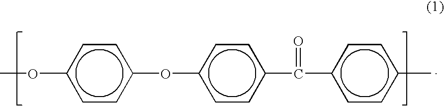
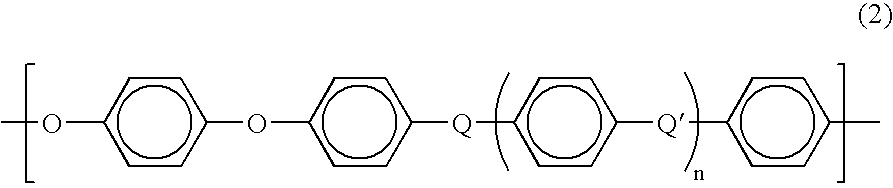
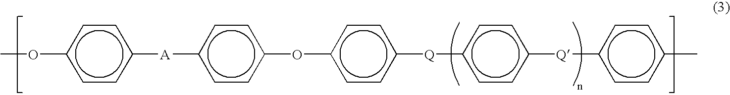
Polyetheretherketone (PEEK) is a high-performance thermoplastic polymer with excellent mechanical properties, chemical resistance, and thermal stability. Various methods for synthesizing PEEK polymers involve specific reaction conditions and catalysts to achieve desired molecular weights and properties. These synthesis approaches can include nucleophilic substitution reactions between diphenols and activated dihalides, often requiring high temperatures and specialized solvents.- PEEK polymer composition and synthesis: Polyetheretherketone (PEEK) is a high-performance thermoplastic polymer with excellent mechanical properties, chemical resistance, and thermal stability. Various methods for synthesizing PEEK polymers have been developed, including nucleophilic substitution reactions and condensation polymerization. The synthesis typically involves the reaction of diphenols with dihalides in the presence of catalysts under controlled conditions to achieve desired molecular weight and properties.
- PEEK polymer blends and composites: PEEK polymers can be blended with other materials or reinforced with fillers to enhance specific properties. Common reinforcements include carbon fibers, glass fibers, and mineral fillers, which significantly improve mechanical strength, stiffness, and dimensional stability. These composites find applications in aerospace, automotive, and industrial sectors where high performance under extreme conditions is required.
- PEEK polymer applications in medical devices: PEEK polymers are widely used in medical applications due to their biocompatibility, radiolucency, and mechanical properties similar to human bone. They are employed in implantable devices, orthopedic implants, spinal cages, and dental prosthetics. Medical-grade PEEK can be sterilized using conventional methods without significant degradation of properties, making it suitable for long-term implantation in the human body.
- PEEK polymer processing techniques: Various processing techniques can be applied to PEEK polymers, including injection molding, extrusion, compression molding, and additive manufacturing. Due to its high melting point (around 343°C), specialized equipment and processing conditions are required. Surface treatments and modifications can be applied to enhance adhesion properties, wettability, or to incorporate functional groups for specific applications.
- PEEK polymer in filtration and separation systems: PEEK polymers are utilized in filtration and separation systems due to their excellent chemical resistance, thermal stability, and mechanical strength. They are employed in membrane supports, filter housings, and components for high-temperature or chemically aggressive environments. PEEK-based filtration systems can withstand harsh operating conditions, including high temperatures, pressures, and exposure to corrosive chemicals, making them suitable for industrial and pharmaceutical applications.
02 PEEK polymer blends and composites
PEEK can be blended with other materials to enhance specific properties or create composites with superior performance characteristics. These blends may incorporate carbon fibers, glass fibers, or other polymers to improve mechanical strength, wear resistance, or thermal conductivity. The resulting composites find applications in aerospace, automotive, and industrial sectors where high performance under extreme conditions is required.Expand Specific Solutions03 PEEK polymer for medical applications
PEEK polymers have gained significant importance in medical and biomedical applications due to their biocompatibility, radiolucency, and mechanical properties similar to human bone. These materials are used in implantable medical devices, dental applications, and surgical instruments. Modified PEEK formulations can include antimicrobial properties or enhanced osseointegration capabilities for improved clinical outcomes.Expand Specific Solutions04 PEEK polymer processing techniques
Various processing techniques are employed for PEEK polymers, including injection molding, extrusion, compression molding, and additive manufacturing. These processes require specific temperature profiles, pressure conditions, and cooling rates to achieve optimal part quality. Advanced processing methods have been developed to overcome challenges associated with PEEK's high melting point and viscosity, enabling the production of complex geometries with consistent properties.Expand Specific Solutions05 PEEK polymer for filtration and separation applications
PEEK polymers are utilized in filtration and separation technologies due to their excellent chemical resistance, thermal stability, and mechanical strength. These materials are processed into membranes, filters, and support structures for applications in harsh chemical environments, high-temperature operations, and critical separation processes. PEEK-based filtration systems offer advantages in industries requiring pure water, pharmaceutical processing, and chemical manufacturing.Expand Specific Solutions
Leading PEEK and MEMS Industry Players
The MEMS technology market utilizing PEEK polymers is currently in a growth phase, with increasing adoption across medical devices, aerospace, and electronics sectors. The market size is estimated to reach significant value due to PEEK's exceptional thermal stability, chemical resistance, and mechanical properties. In terms of technical maturity, leading players like Solvay Specialty Polymers, Victrex Manufacturing, and Jilin Joinature Polymer have established advanced capabilities in PEEK formulation for MEMS applications. Academic institutions including Jilin University and Zhejiang University are driving fundamental research, while companies like Stryker and Olympus are implementing PEEK-based MEMS in medical devices. The competitive landscape shows a balance between established chemical corporations and specialized polymer manufacturers, with increasing collaboration between industry and academic research centers to overcome processing challenges.
Victrex Manufacturing Ltd.
Technical Solution: Victrex has pioneered APTIV® film technology, a specialized PEEK-based solution engineered specifically for MEMS applications requiring exceptional dimensional stability and thermal resistance. Their proprietary manufacturing process creates ultra-thin PEEK films (down to 6 microns) with highly controlled thickness uniformity (±5%), critical for precise MEMS device fabrication. Victrex's PEEK formulations incorporate nanoscale fillers that enhance mechanical properties while maintaining processability, achieving flexural moduli exceeding 4 GPa while preserving the polymer's inherent chemical resistance. Their technology includes specialized surface treatment protocols that improve adhesion to metals and silicon, enabling reliable integration with traditional MEMS materials. Victrex has developed PEEK composites with tailored coefficients of thermal expansion (CTE) ranging from 25-47 ppm/K, allowing better matching with other MEMS structural materials to minimize thermal stress during operation.
Strengths: Victrex offers unmatched expertise in PEEK processing and formulation, with materials demonstrating exceptional mechanical properties retention at elevated temperatures. Their established supply chain and quality control systems ensure consistent performance across production batches. Weaknesses: Limited electrical conductivity options compared to some competing materials, and relatively high material costs that can impact overall MEMS device economics for high-volume applications.
Jilin Joinature Polymer Co., Ltd.
Technical Solution: Jilin Joinature has developed a proprietary PEEK synthesis process optimized for MEMS applications, yielding polymers with molecular weights exceeding 80,000 g/mol and polydispersity indices below 2.3, ensuring consistent mechanical properties critical for MEMS device reliability. Their technology includes specialized PEEK composites incorporating silicon carbide nanoparticles (3-5% by weight) that enhance tribological properties while maintaining processability, achieving friction coefficients as low as 0.15 in dry conditions. The company has pioneered solvent-based PEEK processing techniques that enable direct patterning of PEEK structures with feature sizes down to 10μm, compatible with standard photolithography equipment. Their MEMS-grade PEEK materials demonstrate glass transition temperatures consistently above 145°C and crystallinity levels between 30-35%, providing excellent dimensional stability during thermal cycling typical in MEMS operation environments.
Strengths: Cost-effective manufacturing processes make their PEEK materials more accessible for commercial MEMS applications, and their materials show excellent chemical compatibility with standard MEMS processing chemicals. Weaknesses: Less established global presence compared to Western competitors limits technical support availability, and their materials have less documented long-term reliability data in mission-critical applications.
Key PEEK Material Innovations for MEMS Technology
Semiconductive film, electric charge control member and process for production the semiconductive film
PatentInactiveUS20070020450A1
Innovation
- A production process involving extrusion of a resin composition comprising PEEK and a conductive filler through a T-die or ring die with controlled lip clearance and temperature, followed by cooling and solidification using a cooling roll or mandrel, to produce a semiconductive film with balanced properties including narrow thickness and volume resistivity scatter, high folding endurance, and excellent mechanical strength.
A polyether ether ketone-based composite, and methods thereof
PatentActiveIN201811018806A
Innovation
- A composite material comprising polyether ether ketone (PEEK) reinforced with refractory materials like silicon carbide (SiC) and a compatibilizer like polycarbosilane, with a refractory to PEEK weight ratio of 0.001:1 to 0.42:1, to improve hardness and flame-retardancy.
Environmental Impact of PEEK in MEMS Manufacturing
The environmental impact of PEEK (Polyetheretherketone) in MEMS manufacturing represents a critical consideration as this high-performance polymer gains traction in microelectromechanical systems technology. PEEK offers significant environmental advantages compared to traditional materials used in MEMS fabrication. Its exceptional chemical resistance eliminates the need for toxic protective coatings, reducing hazardous waste generation during manufacturing processes.
PEEK-based MEMS production typically consumes less energy than conventional silicon or metal-based manufacturing, as PEEK can be processed at lower temperatures (around 343°C compared to silicon's 1400°C processing requirements). This temperature differential translates to substantial energy savings and reduced carbon emissions across production facilities. Additionally, PEEK manufacturing processes generate fewer harmful byproducts compared to traditional semiconductor fabrication, which often involves hazardous chemicals like hydrofluoric acid and various heavy metals.
The durability and longevity of PEEK components contribute positively to the environmental profile of MEMS devices. With superior resistance to thermal cycling, mechanical stress, and chemical degradation, PEEK-based MEMS typically exhibit extended operational lifespans, reducing replacement frequency and associated electronic waste. This longevity factor becomes increasingly important as miniaturized electronic systems proliferate across consumer and industrial applications.
From a lifecycle perspective, PEEK presents both advantages and challenges. While its exceptional durability reduces replacement waste, end-of-life recycling remains problematic. PEEK's high thermal stability and chemical resistance—the very properties that make it valuable for MEMS applications—also complicate conventional recycling processes. Current mechanical recycling methods for PEEK result in significant property degradation, limiting closed-loop recycling potential.
Water consumption in PEEK-based MEMS manufacturing deserves particular attention. Compared to traditional silicon processing, which requires ultra-pure water in substantial quantities, PEEK fabrication typically demands less water. However, the polymer processing still requires cooling systems and cleaning processes that consume water resources, though advanced facilities are implementing closed-loop water recycling systems to mitigate this impact.
Emerging research focuses on developing more environmentally sustainable PEEK formulations specifically for MEMS applications. Bio-based precursors and additives are being explored to reduce the polymer's petroleum dependence, while maintaining its exceptional performance characteristics. Additionally, novel manufacturing techniques like additive manufacturing (3D printing) of PEEK components show promise for reducing material waste through more precise deposition processes, potentially decreasing the environmental footprint of PEEK-based MEMS production.
Thermal and Chemical Stability Considerations
PEEK (polyetheretherketone) polymer exhibits exceptional thermal stability, maintaining structural integrity at temperatures up to 260°C continuously and withstanding short-term exposure to temperatures approaching 300°C. This remarkable thermal resistance makes PEEK an ideal candidate for MEMS applications requiring operation in harsh thermal environments, such as automotive sensors, aerospace components, and industrial monitoring systems. Unlike conventional polymers that degrade rapidly at elevated temperatures, PEEK's aromatic backbone structure provides inherent resistance to thermal decomposition, ensuring consistent performance across wide temperature ranges.
The chemical stability of PEEK further enhances its suitability for MEMS technology. The polymer demonstrates outstanding resistance to a broad spectrum of chemicals, including acids, bases, hydrocarbons, and organic solvents. This resistance is particularly valuable in microfluidic MEMS applications where exposure to aggressive reagents is common. PEEK's chemical inertness prevents degradation that could compromise device functionality or introduce contamination in sensitive analytical processes. Studies have shown that PEEK maintains its mechanical properties even after prolonged exposure to harsh chemicals that would rapidly degrade alternative polymers.
Radiation stability represents another critical consideration for PEEK in MEMS applications. The polymer exhibits superior resistance to various forms of radiation, including gamma rays and UV exposure, making it suitable for space applications and medical devices requiring sterilization. This radiation resistance prevents chain scission and cross-linking phenomena that typically compromise the mechanical integrity of polymers in radiation-intensive environments.
The hydrolytic stability of PEEK is exceptional, with minimal water absorption (typically less than 0.5% by weight) and resistance to hydrolysis even in high-temperature aqueous environments. This property is crucial for MEMS devices operating in humid conditions or biological environments, as it ensures dimensional stability and consistent electrical properties over time. The low moisture uptake also contributes to PEEK's excellent electrical insulation characteristics, which remain stable across varying humidity levels.
When considering long-term reliability, PEEK demonstrates minimal aging effects compared to other engineering polymers. Accelerated aging tests have shown that PEEK maintains its mechanical and thermal properties after extended exposure to elevated temperatures and oxidative environments. This stability translates to extended service life for PEEK-based MEMS devices, reducing replacement frequency and associated costs in critical applications.
The combination of these stability characteristics positions PEEK as a superior material for MEMS applications where environmental resistance is paramount. However, processing considerations must be addressed, as PEEK's high melting temperature (approximately 343°C) and limited solubility in common solvents present challenges for conventional microfabrication techniques. Advanced processing methods, including laser micromachining and specialized molding techniques, have been developed to overcome these limitations and fully leverage PEEK's exceptional stability profile in next-generation MEMS devices.
Unlock deeper insights with PatSnap Eureka Quick Research — get a full tech report to explore trends and direct your research. Try now!
Generate Your Research Report Instantly with AI Agent
Supercharge your innovation with PatSnap Eureka AI Agent Platform!