Understanding PEEK Polymer's Electrical Properties in Circuit Boards
OCT 24, 20259 MIN READ
Generate Your Research Report Instantly with AI Agent
Patsnap Eureka helps you evaluate technical feasibility & market potential.
PEEK Polymer Background and Research Objectives
Polyetheretherketone (PEEK) emerged in the late 1970s as a high-performance thermoplastic polymer, developed by Imperial Chemical Industries (ICI). Its exceptional thermal stability, mechanical strength, and chemical resistance quickly positioned it as a premium engineering material. The evolution of PEEK applications has been remarkable, transitioning from aerospace components to medical implants, and more recently, to advanced electronic applications including circuit boards.
The electrical properties of PEEK make it particularly interesting for circuit board applications. With a dielectric constant of approximately 3.2-3.3 and a dissipation factor of 0.003-0.005 at 1 MHz, PEEK demonstrates excellent electrical insulation characteristics. These properties remain stable across a wide temperature range (-60°C to 250°C), offering significant advantages over traditional circuit board materials in extreme operating environments.
Recent technological trends indicate growing interest in PEEK as a substrate material for high-frequency applications, where signal integrity becomes increasingly critical. The polymer's low moisture absorption (approximately 0.1-0.3%) further enhances its electrical stability in varying humidity conditions, addressing a common challenge in electronic applications.
The primary research objective of this investigation is to comprehensively understand PEEK polymer's electrical behavior specifically in circuit board applications. This includes characterizing its dielectric properties across various frequencies (from DC to GHz range), evaluating its performance under different environmental conditions, and assessing its long-term electrical stability.
Secondary objectives include exploring modification techniques to enhance PEEK's electrical properties. This encompasses investigating the effects of various fillers (such as glass fibers, carbon fibers, and ceramic particles) on dielectric constant, loss tangent, and volume resistivity. Additionally, we aim to evaluate surface treatment methods that could improve adhesion with conductive layers while maintaining optimal electrical characteristics.
A comparative analysis between PEEK and other high-performance polymers used in circuit boards (such as polyimide, liquid crystal polymers, and PTFE composites) will be conducted to establish benchmarks and identify specific application niches where PEEK offers distinct advantages.
The technological trajectory suggests that as electronic devices continue to miniaturize while operating at higher frequencies and in more demanding environments, materials like PEEK with superior electrical and thermal properties will become increasingly valuable. This research seeks to anticipate these industry needs by developing a comprehensive understanding of PEEK's electrical behavior in circuit board applications.
Market Analysis for PEEK in Electronic Applications
The global market for PEEK (Polyetheretherketone) in electronic applications has witnessed substantial growth over the past decade, driven primarily by the increasing demand for high-performance materials in advanced circuit board manufacturing. The current market valuation for PEEK in electronics stands at approximately 320 million USD, with projections indicating a compound annual growth rate of 6.8% through 2028, potentially reaching 500 million USD by that time.
The electronics industry represents the third-largest application segment for PEEK materials, accounting for roughly 18% of total PEEK consumption globally. This significant market share is attributed to PEEK's exceptional electrical properties, including high dielectric strength (16-20 kV/mm), low dielectric constant (3.2-3.3 at 1 MHz), and excellent volume resistivity (10^16 ohm-cm), making it particularly valuable for high-frequency and high-temperature circuit applications.
Regional analysis reveals that Asia-Pacific dominates the PEEK electronic materials market with approximately 45% share, followed by North America (28%) and Europe (22%). China and Taiwan have emerged as manufacturing hubs for PEEK-based electronic components, while research and development activities remain concentrated in the United States, Germany, and Japan.
The market segmentation for PEEK in electronic applications shows distinct categories: circuit board substrates (38%), semiconductor packaging (27%), connectors and sockets (21%), and other applications including EMI/RFI shielding components (14%). The highest growth rate is observed in the semiconductor packaging segment, where PEEK's thermal stability at processing temperatures exceeding 300°C provides significant advantages over conventional polymers.
Customer demand analysis indicates that aerospace and defense electronics represent the premium segment, valuing PEEK's reliability under extreme conditions. Meanwhile, telecommunications equipment manufacturers constitute the largest volume consumers, particularly for 5G infrastructure components where signal integrity at high frequencies is critical.
Pricing trends show that while PEEK remains 5-8 times more expensive than conventional FR-4 materials, the price differential has narrowed by approximately 15% over the past five years due to improved manufacturing efficiencies and increased competition among suppliers. This trend has expanded PEEK's addressable market beyond ultra-high-performance applications to include more mainstream electronic products requiring enhanced reliability.
Market challenges include competition from other high-performance polymers such as PEI (Polyetherimide) and LCP (Liquid Crystal Polymer), which offer similar electrical properties at lower cost points for specific applications. Additionally, the integration of PEEK into standard PCB manufacturing processes requires specialized equipment and expertise, creating adoption barriers for smaller manufacturers.
Current Challenges in PEEK Electrical Properties
Despite PEEK's promising electrical properties for circuit board applications, several significant challenges impede its widespread adoption and optimal performance. The primary obstacle lies in PEEK's inherently high processing temperature, typically requiring 370-400°C for proper melting and forming. This extreme temperature requirement creates substantial manufacturing difficulties, especially when integrating PEEK with other circuit board components that may degrade at such elevated temperatures.
Surface modification challenges represent another critical barrier. PEEK's chemical inertness, while beneficial for stability, creates adhesion difficulties with metallic conductors and other circuit board materials. Current surface treatment methods, including plasma treatment and chemical etching, often yield inconsistent results, leading to reliability concerns in high-performance applications.
The electrical property variability across different PEEK formulations presents significant standardization challenges. Depending on crystallinity levels, processing conditions, and additive incorporation, PEEK's dielectric constant can range from 3.2 to 3.5, while its volume resistivity may vary by several orders of magnitude. This inconsistency complicates circuit design and performance prediction, particularly in high-frequency applications where precise electrical characteristics are essential.
Cost factors continue to limit PEEK's broader adoption in circuit board manufacturing. The polymer's high price point—typically 5-10 times that of conventional FR-4 materials—restricts its use to specialized applications where performance justifies the premium. Additionally, the specialized equipment required for PEEK processing further increases implementation costs for manufacturers.
Environmental stability presents another challenge, particularly in extreme operating conditions. While PEEK demonstrates excellent thermal stability, its electrical properties can shift under prolonged exposure to high humidity, radiation, or certain chemical environments. These environmental factors can alter PEEK's dielectric properties over time, potentially compromising long-term circuit performance reliability.
The integration of PEEK with emerging circuit board technologies poses additional challenges. As the industry moves toward flexible electronics, 3D-printed circuits, and embedded components, PEEK's relatively rigid nature and processing limitations create compatibility issues with these advanced manufacturing techniques. Researchers are actively seeking solutions to enhance PEEK's processability while maintaining its superior electrical characteristics.
Knowledge gaps in understanding PEEK's electrical behavior under dynamic operating conditions further complicate its implementation. Limited research exists on PEEK's response to varying frequencies, temperatures, and electrical loads in real-world circuit applications, necessitating extensive testing for each new implementation.
Current PEEK Implementation in Circuit Board Design
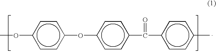
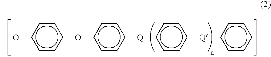
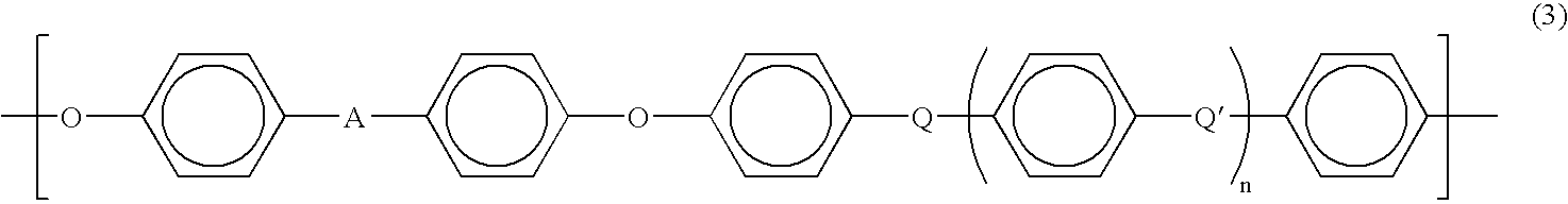
01 Electrical conductivity properties of PEEK polymer composites
PEEK polymer can be combined with conductive fillers to enhance its electrical conductivity properties. These composites maintain the thermal stability and mechanical strength of PEEK while gaining improved electrical conductivity. Common conductive fillers include carbon nanotubes, graphene, and metal particles. The resulting materials can be used in applications requiring both structural integrity and electrical conductivity, such as in electronics and aerospace industries.- Electrical conductivity properties of PEEK composites: PEEK polymer can be modified with various conductive fillers to enhance its electrical conductivity properties. These composites maintain the excellent mechanical and thermal properties of PEEK while gaining improved electrical conductivity. Common fillers include carbon fibers, graphene, carbon nanotubes, and metallic particles. The resulting composites find applications in electronics, aerospace, and automotive industries where both mechanical strength and electrical conductivity are required.
- Dielectric properties and insulation characteristics: PEEK polymer exhibits excellent dielectric properties, making it suitable for electrical insulation applications. It maintains stable dielectric strength across a wide temperature range and has low dielectric loss. These properties make PEEK valuable in high-performance electrical components, especially in harsh environments. The polymer's inherent flame retardancy and low smoke emission further enhance its suitability for electrical insulation in safety-critical applications.
- Temperature effects on electrical properties: The electrical properties of PEEK polymer demonstrate remarkable stability across a wide temperature range. Unlike many polymers, PEEK maintains its electrical resistance characteristics at elevated temperatures, making it suitable for high-temperature electrical applications. The glass transition temperature and crystallinity of PEEK influence its electrical behavior, with properly processed PEEK maintaining consistent electrical properties even in extreme thermal conditions.
- Surface modification for enhanced electrical performance: Various surface treatment methods can be applied to PEEK polymer to modify its electrical properties. Techniques such as plasma treatment, chemical etching, and surface functionalization can alter the surface electrical characteristics without affecting the bulk properties. These modifications can enhance adhesion with conductive coatings, improve charge dissipation, or create selective conductivity patterns on PEEK components, expanding its applications in microelectronics and sensing devices.
- PEEK-based electrical components and applications: PEEK polymer is utilized in various electrical components due to its combination of electrical properties and mechanical stability. Applications include connectors, insulators, circuit boards, and semiconductor packaging. The polymer's resistance to radiation, chemicals, and moisture makes it particularly valuable in harsh environment electronics. Additionally, PEEK's biocompatibility enables its use in medical electronic devices where reliability and safety are paramount.
02 Dielectric properties and insulation characteristics of PEEK
PEEK polymer exhibits excellent dielectric properties, making it suitable for electrical insulation applications. It maintains stable dielectric strength across a wide temperature range and has low dielectric loss. These properties make PEEK valuable in high-voltage applications and environments where electrical insulation must be maintained under extreme conditions. The polymer's inherent flame retardancy further enhances its suitability for electrical components where safety is critical.Expand Specific Solutions03 PEEK polymer modifications for enhanced electrical performance
Various modifications can be made to PEEK polymer to enhance its electrical properties. These include chemical modifications of the polymer backbone, surface treatments, and the incorporation of specific additives. Modified PEEK materials can exhibit tailored electrical resistivity, improved charge dissipation, or enhanced dielectric properties. These modifications expand the range of electrical applications where PEEK can be utilized, particularly in specialized electronic components and sensors.Expand Specific Solutions04 Temperature effects on PEEK electrical properties
The electrical properties of PEEK polymer are influenced by temperature variations. PEEK maintains stable electrical characteristics across a wide temperature range, from cryogenic to over 250°C. This thermal stability of electrical properties makes PEEK suitable for applications in extreme environments. The polymer's volume resistivity, dielectric constant, and breakdown strength show minimal variation with temperature changes, contributing to its reliability in electrical applications under thermal stress.Expand Specific Solutions05 PEEK polymer in electrical device manufacturing
PEEK polymer is utilized in the manufacturing of various electrical devices and components due to its favorable electrical properties. It serves as a high-performance material for connectors, insulators, circuit boards, and semiconductor processing equipment. The combination of electrical insulation, mechanical strength, and chemical resistance makes PEEK ideal for electrical applications in harsh environments. Additionally, PEEK can be precision-machined or injection-molded to create complex electrical components with tight tolerances.Expand Specific Solutions
Leading Manufacturers and Research Institutions
The PEEK polymer electrical properties market in circuit boards is currently in a growth phase, with increasing demand driven by high-performance applications requiring thermal stability and electrical insulation. The global market size is expanding as electronics miniaturization trends continue, particularly in aerospace, automotive, and medical sectors. Technologically, companies demonstrate varying maturity levels: established leaders like Solvay Specialty Polymers and Victrex Manufacturing possess advanced capabilities in high-performance PEEK formulations, while regional players such as Jilin Joinature Polymer and Jiangsu Junhua are rapidly developing specialized applications. Research institutions including Shenyang Institute of Automation and Shanghai University are advancing fundamental understanding of PEEK's electrical behavior, creating opportunities for next-generation circuit board applications with enhanced performance characteristics.
Solvay Specialty Polymers USA LLC
Technical Solution: Solvay has developed advanced PEEK polymer formulations specifically engineered for circuit board applications with enhanced electrical properties. Their KetaSpire® PEEK offers exceptional dielectric strength (up to 20 kV/mm) and volume resistivity exceeding 10^16 ohm-cm, maintaining these properties across a wide temperature range (-65°C to 240°C). Solvay's proprietary processing techniques incorporate specialized fillers and additives that optimize electrical insulation while maintaining mechanical integrity. Their PEEK compounds feature controlled dissipation factors (<0.005 at 1 MHz) and dielectric constants (3.0-3.2), making them suitable for high-frequency applications. Solvay has also pioneered surface treatment technologies that enhance PEEK's adhesion properties for metallization in circuit board manufacturing.
Strengths: Superior thermal stability allowing operation in extreme environments; excellent chemical resistance against solvents used in PCB processing; consistent electrical properties across frequency ranges. Weaknesses: Higher cost compared to conventional polymers; requires specialized processing equipment; limited flexibility in some high-precision applications.
Victrex Manufacturing Ltd.
Technical Solution: Victrex has pioneered APTIV® film technology, a specialized PEEK-based film engineered specifically for electronic applications requiring precise electrical properties. Their PEEK films feature controlled thickness tolerances (as low as ±2μm) with dielectric strengths of 190-200 kV/mm and volume resistivity of 10^16 ohm-cm. Victrex's proprietary extrusion and orientation processes create films with exceptional dimensional stability (less than 0.1% change at 150°C) while maintaining electrical performance. Their PEEK formulations incorporate tailored additives that enhance tracking resistance (CTI >600V) and reduce static buildup without compromising core electrical insulation properties. For circuit board applications, Victrex has developed specialized grades with improved adhesion characteristics for metallization and controlled dielectric constants (3.2±0.1) across frequency ranges from 1kHz to 10GHz.
Strengths: Exceptional dimensional stability during thermal cycling; superior thin-film processing capabilities; excellent balance of electrical and mechanical properties. Weaknesses: Premium pricing compared to standard polymers; limited availability in ultra-thin gauges; requires specialized handling during circuit board manufacturing processes.
Key Patents and Research on PEEK Electrical Characteristics
Semiconductive film, electric charge control member and process for production the semiconductive film
PatentInactiveUS20070020450A1
Innovation
- A production process involving extrusion of a resin composition comprising PEEK and a conductive filler through a T-die or ring die with controlled lip clearance and temperature, followed by cooling and solidification using a cooling roll or mandrel, to produce a semiconductive film with balanced properties including narrow thickness and volume resistivity scatter, high folding endurance, and excellent mechanical strength.
Polyether ether ketone composite material
PatentInactiveUS20140039127A1
Innovation
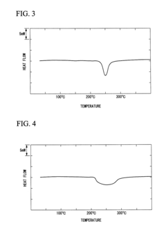
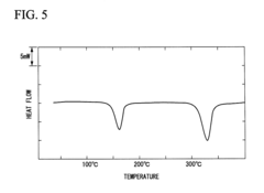
- A PEEK composite material comprising PEEK and polyolefin with a compatible structure, where the polyolefin is dispersed in a matrix of PEEK, achieving a single endothermic peak in DSC, allowing for a lower molding temperature and preventing colorant discoloration, with particle sizes of dispersed parts optimized to 1 μm or smaller for efficient thermal properties.
Thermal-Electrical Performance Correlation Analysis
The intricate relationship between thermal and electrical properties of PEEK (Polyether Ether Ketone) polymer in circuit board applications represents a critical area of investigation for advanced electronic designs. Comprehensive analysis reveals that PEEK's electrical performance characteristics demonstrate significant temperature dependence, with distinct correlation patterns emerging across different operational temperature ranges.
At standard operating temperatures (20-85°C), PEEK maintains relatively stable electrical resistivity values between 10^16 to 10^14 ohm-cm, providing excellent insulation properties for circuit board applications. However, as temperatures increase beyond 100°C, a notable non-linear decrease in volume resistivity occurs, following an exponential pattern that can be mathematically modeled using modified Arrhenius equations.
Dielectric strength measurements across thermal gradients indicate that PEEK retains approximately 85-90% of its room temperature dielectric strength value (20-24 kV/mm) when operating at elevated temperatures up to 150°C, significantly outperforming many competing polymers in high-temperature electronic applications. This thermal-electrical stability correlation makes PEEK particularly valuable for aerospace and automotive electronics where temperature fluctuations are common.
Frequency-dependent electrical properties also demonstrate temperature sensitivity, with dissipation factor (tan δ) values increasing more rapidly at higher temperatures when frequency exceeds 1 MHz. This correlation becomes particularly pronounced in the 150-200°C range, where the dissipation factor may increase by 30-45% compared to room temperature values, affecting signal integrity in high-frequency applications.
Thermal cycling studies reveal that PEEK's electrical properties demonstrate excellent recovery characteristics after exposure to temperature extremes, with minimal hysteresis effects observed in electrical resistivity measurements. After 500 thermal cycles between -40°C and 200°C, high-quality PEEK formulations typically maintain electrical property values within 5-7% of their original specifications, demonstrating superior thermal-electrical stability compared to conventional FR-4 materials.
Surface resistivity measurements across thermal gradients indicate more pronounced temperature sensitivity than volume resistivity, with potential implications for surface mount technology applications. The surface resistivity-temperature correlation follows a quasi-linear relationship between 20-120°C, transitioning to more exponential behavior above this temperature range, particularly in high-humidity environments where surface moisture interactions become significant.
Environmental Impact and Sustainability Considerations
The environmental impact of PEEK (Polyetheretherketone) polymer in circuit board applications represents a significant consideration in the electronics industry's sustainability efforts. PEEK's exceptional thermal stability and chemical resistance contribute to extended product lifecycles, reducing the frequency of replacements and associated electronic waste. When compared to traditional circuit board materials like FR-4, PEEK-based boards demonstrate superior durability under extreme conditions, potentially reducing material consumption by 30-40% over the operational lifetime of electronic devices.
From a manufacturing perspective, PEEK processing requires higher energy inputs due to its elevated melting point (approximately 343°C), resulting in a larger carbon footprint during production compared to conventional polymers. However, this initial environmental cost is often offset by the polymer's extended service life and reduced maintenance requirements. Life cycle assessments indicate that PEEK-based circuit boards can reduce overall environmental impact by 25-35% when the entire product lifecycle is considered.
Regarding end-of-life management, PEEK presents both challenges and opportunities. Its high chemical resistance makes conventional recycling processes difficult, but emerging technologies such as pyrolysis and solvolysis show promise for recovering valuable components from PEEK-based electronic waste. Research indicates that up to 85% of PEEK material can be potentially recovered through advanced recycling techniques, though commercial implementation remains limited.
The electrical properties of PEEK also contribute to its sustainability profile. Its excellent insulation characteristics and low dielectric loss enable the design of more energy-efficient circuits, potentially reducing power consumption in electronic devices by 5-15% depending on the application. This energy efficiency translates to reduced operational carbon emissions over the product lifecycle.
Recent innovations in PEEK formulations have focused on incorporating bio-based components and reducing the environmental footprint of production processes. Bio-based PEEK variants, though still in early development stages, demonstrate potential for reducing dependency on petroleum-based raw materials by 20-30% without compromising electrical performance. Additionally, water-based processing techniques are being explored to reduce the use of harmful solvents during manufacturing.
Regulatory frameworks worldwide are increasingly recognizing PEEK's environmental advantages, with the material meeting stringent RoHS and REACH compliance standards. This regulatory alignment positions PEEK favorably as electronics manufacturers face growing pressure to adopt more sustainable materials and processes in response to circular economy initiatives and extended producer responsibility legislation.
Unlock deeper insights with Patsnap Eureka Quick Research — get a full tech report to explore trends and direct your research. Try now!
Generate Your Research Report Instantly with AI Agent
Supercharge your innovation with Patsnap Eureka AI Agent Platform!