

How do Gallium Nitride Transistors Enhance Aerospace Electronics
OCT 14, 202510 MIN READ
Generate Your Research Report Instantly with AI Agent
PatSnap Eureka helps you evaluate technical feasibility & market potential.
GaN Transistor Evolution and Aerospace Applications
The evolution of Gallium Nitride (GaN) transistor technology represents a significant paradigm shift in aerospace electronics. Since the early 2000s, GaN has emerged from laboratory research to become a cornerstone technology in high-performance aerospace applications. The wide bandgap semiconductor properties of GaN, with its 3.4 eV bandgap compared to silicon's 1.1 eV, enable operation at higher voltages, frequencies, and temperatures than conventional silicon-based technologies.
The developmental trajectory of GaN transistors has been marked by several key milestones. Initial research focused on overcoming material growth challenges, particularly the lack of native substrates. The breakthrough came with the development of heteroepitaxial growth techniques on silicon carbide and sapphire substrates, enabling commercially viable production. By 2005, the first reliable GaN high-electron-mobility transistors (HEMTs) demonstrated power densities exceeding 10 W/mm, far surpassing silicon capabilities.
In aerospace applications, GaN transistors have revolutionized radar systems, satellite communications, and electronic warfare equipment. Modern airborne radar systems utilizing GaN technology have achieved 5-10 times the power output of previous gallium arsenide solutions while reducing size and weight by approximately 30%. This translates directly to extended detection ranges and improved resolution for critical aerospace systems.
The integration of GaN in satellite communications has enabled higher data transmission rates and more efficient power amplification. Current GaN-based solid-state power amplifiers (SSPAs) achieve efficiencies exceeding 70% at Ka-band frequencies, compared to 40-50% for traditional technologies. This efficiency improvement has dramatically reduced thermal management requirements and extended satellite operational lifespans.
For electronic warfare applications, GaN transistors provide unprecedented bandwidth capabilities, enabling systems to operate across multiple frequency bands simultaneously. This versatility is crucial for modern aerospace platforms that must function in increasingly congested electromagnetic environments. GaN-based jammers and countermeasure systems can generate higher output power across broader frequency ranges, enhancing aircraft survivability.
The reliability improvements in GaN technology have been equally impressive. Modern GaN devices demonstrate mean time to failure exceeding 10^7 hours at operating temperatures of 200°C, addressing the stringent reliability requirements of aerospace applications. This exceptional reliability, combined with radiation hardness superior to silicon alternatives, makes GaN particularly suitable for space applications where component replacement is impossible.
Looking forward, GaN transistor technology continues to evolve toward higher frequencies, greater power densities, and improved thermal performance. Recent developments in diamond-GaN composites promise to push power densities beyond 40 W/mm while maintaining reliability at elevated temperatures, further expanding the application space in next-generation aerospace systems.
Aerospace Electronics Market Demand Analysis
The aerospace electronics market is experiencing unprecedented growth, driven by increasing demand for advanced avionics systems, satellite communications, and defense applications. Current market valuations place the global aerospace electronics sector at approximately $6.3 billion in 2023, with projections indicating a compound annual growth rate of 7.2% through 2030. This expansion is primarily fueled by the modernization of military aircraft fleets, growing commercial aviation sectors in emerging economies, and increased investment in space exploration initiatives.
Within this expanding market, there exists a critical demand for electronic components that can withstand extreme environmental conditions while delivering superior performance. Aerospace applications typically operate under harsh conditions including temperature extremes ranging from -55°C to over 200°C, high radiation exposure, and significant vibration stress. Traditional silicon-based electronics struggle to maintain reliability under these conditions, creating a substantial market gap for more robust alternatives.
Power management systems represent a particularly high-demand segment, with aerospace manufacturers seeking solutions that can reduce weight, increase efficiency, and enhance reliability. The industry's push toward more electric aircraft (MEA) architectures has intensified this need, as modern aircraft designs incorporate increasingly sophisticated electronic systems that replace traditional hydraulic and pneumatic controls.
Market research indicates that aerospace customers are willing to pay premium prices for electronic components that can demonstrate tangible improvements in three key performance metrics: power density, thermal management, and radiation hardness. Gallium Nitride (GaN) transistors directly address these requirements, positioning them as highly valuable components in the aerospace supply chain.
Regional analysis reveals varying demand patterns, with North America leading in defense-related applications of advanced electronics, while Europe shows stronger interest in commercial aviation applications. The Asia-Pacific region, particularly China and India, represents the fastest-growing market segment, driven by ambitious space programs and expanding defense budgets.
Industry surveys indicate that aerospace manufacturers prioritize long-term reliability over initial cost considerations, creating favorable market conditions for premium solutions like GaN transistors. The typical procurement cycle for aerospace electronics components spans 2-3 years, with qualification testing representing a significant portion of this timeline. This extended qualification process creates substantial barriers to entry but also ensures strong market positions for technologies that successfully navigate certification requirements.
The shift toward unmanned aerial vehicles (UAVs) and small satellite constellations has created new market opportunities for specialized electronic components that can deliver high performance in compact form factors. These emerging applications value power efficiency and heat dissipation capabilities—areas where GaN technology demonstrates significant advantages over conventional solutions.
GaN Technology Status and Implementation Challenges
Gallium Nitride (GaN) technology has emerged as a revolutionary material in power electronics, offering significant advantages over traditional silicon-based semiconductors. Currently, GaN transistors have reached commercial maturity in several sectors, with aerospace applications representing one of the most promising yet challenging implementation areas. The global market for GaN power devices is experiencing rapid growth, projected to reach $1.75 billion by 2026 with a CAGR of approximately 35%.
In aerospace electronics specifically, GaN technology has demonstrated superior performance in radar systems, satellite communications, and electronic warfare applications. However, widespread adoption faces several critical challenges. The primary technical hurdle remains thermal management, as GaN devices generate significant heat during high-power operation in confined aerospace environments. Current cooling solutions often add weight and complexity, counteracting the inherent benefits of GaN's power density advantages.
Reliability concerns present another major challenge, particularly in aerospace applications where component failure is unacceptable. While GaN devices have demonstrated impressive mean time between failures (MTBF) in laboratory settings, long-term reliability data in extreme aerospace conditions remains limited. Radiation hardness testing has shown promising results, but further validation is required for mission-critical applications in space environments.
Manufacturing scalability continues to constrain broader implementation. Current GaN wafer production primarily utilizes silicon carbide (SiC) substrates, which are expensive and limited in supply. Silicon substrates offer cost advantages but introduce performance compromises through lattice mismatch issues. The industry is gradually transitioning toward larger wafer sizes (6-inch becoming standard), but aerospace-grade production volumes remain relatively low, keeping costs elevated.
Geographically, GaN technology development shows distinct regional characteristics. North America leads in defense and aerospace applications, with companies like Northrop Grumman and Raytheon developing proprietary GaN solutions. Europe focuses on space applications through the European Space Agency's GaN initiatives. Meanwhile, Asia (particularly Japan and China) dominates in commercial GaN manufacturing capacity but lags in aerospace-specific implementations.
Standardization represents another significant challenge, as aerospace electronics require strict certification processes. Currently, there is limited consensus on testing protocols specific to GaN devices in aerospace environments. Industry bodies like JEDEC have begun developing standards, but comprehensive aerospace-specific qualification frameworks remain under development.
Cost factors continue to impact adoption rates, with GaN solutions typically commanding a 2.5-3x premium over silicon alternatives. While this gap is narrowing annually (approximately 15% cost reduction per year), aerospace qualification requirements maintain higher price points compared to commercial applications.
Current GaN Solutions for Aerospace Systems
01 GaN HEMT structure optimization
High Electron Mobility Transistors (HEMTs) based on Gallium Nitride can be enhanced through structural optimizations. These include improving the two-dimensional electron gas (2DEG) channel formation, optimizing the AlGaN/GaN heterostructure, and engineering the gate structure to reduce leakage current and increase breakdown voltage. These structural improvements lead to better carrier mobility and higher power density capabilities.- GaN HEMT structure optimization: High Electron Mobility Transistors (HEMTs) based on Gallium Nitride can be enhanced through structural optimizations. These include improving the two-dimensional electron gas (2DEG) channel formation, optimizing the AlGaN/GaN heterostructure, and engineering the gate design. Such optimizations lead to higher electron mobility, reduced on-resistance, and improved switching performance, making these transistors suitable for high-frequency and high-power applications.
- GaN growth and substrate technologies: Enhancement of Gallium Nitride transistors can be achieved through advanced growth techniques and substrate selection. Methods such as Metal-Organic Chemical Vapor Deposition (MOCVD), Molecular Beam Epitaxy (MBE), and Hydride Vapor Phase Epitaxy (HVPE) are used to grow high-quality GaN layers. Various substrates including silicon, silicon carbide, and sapphire are employed, each offering different benefits for thermal management, lattice matching, and cost-effectiveness.
- Gate engineering and dielectric integration: Gate engineering plays a crucial role in enhancing GaN transistor performance. Techniques include implementing recessed gate structures, using novel gate metals, and integrating high-k dielectric materials. These approaches help reduce gate leakage current, improve threshold voltage control, and enhance reliability. Advanced gate technologies also contribute to better channel control and switching characteristics in power applications.
- Power efficiency and thermal management: Enhancing power efficiency and thermal management in GaN transistors involves developing advanced packaging techniques, implementing efficient heat dissipation structures, and optimizing device layouts. These improvements allow GaN transistors to operate at higher power densities while maintaining reliability. Thermal management solutions include flip-chip bonding, diamond heat spreaders, and optimized device geometries that minimize self-heating effects.
- Normally-off GaN transistor technologies: Developing normally-off (enhancement-mode) GaN transistors is critical for power electronics applications. Various approaches include p-GaN gate structures, fluorine plasma treatment, recessed gate configurations, and hybrid cascode structures. These technologies shift the threshold voltage to positive values, enabling safer operation and simpler gate drive requirements compared to conventional depletion-mode devices, while maintaining the high-frequency and high-power density advantages of GaN.
02 GaN growth and substrate technologies
Enhancement of Gallium Nitride transistors can be achieved through improved crystal growth techniques and substrate selection. Methods such as Metal-Organic Chemical Vapor Deposition (MOCVD) and Molecular Beam Epitaxy (MBE) are used to grow high-quality GaN layers. Various substrates including silicon, silicon carbide, and sapphire are employed, each offering different advantages in terms of thermal conductivity, lattice matching, and cost-effectiveness.Expand Specific Solutions03 Surface passivation and gate dielectric engineering
Surface passivation techniques and gate dielectric engineering significantly enhance GaN transistor performance. By applying appropriate passivation layers and optimizing gate dielectrics, issues such as current collapse, dynamic on-resistance, and threshold voltage instability can be mitigated. Materials like SiN, Al2O3, and HfO2 are commonly used to reduce surface states and improve reliability under high-voltage operation.Expand Specific Solutions04 Enhancement-mode GaN transistor designs
Various approaches are used to create enhancement-mode (normally-off) GaN transistors, which are preferred for many power applications. These include p-GaN gate structures, fluorine plasma treatment, recessed gate designs, and hybrid cascode configurations. These techniques modify the threshold voltage to achieve normally-off operation while maintaining the high-performance characteristics of GaN technology.Expand Specific Solutions05 Thermal management and packaging solutions
Effective thermal management and advanced packaging solutions are crucial for enhancing GaN transistor performance. Heat dissipation techniques such as flip-chip bonding, advanced heat sinks, and thermal vias help maintain optimal operating temperatures. Innovative packaging designs reduce parasitic inductances and capacitances, enabling GaN transistors to operate at higher frequencies and power levels with improved reliability.Expand Specific Solutions
Key Players in GaN Aerospace Electronics
Gallium Nitride (GaN) transistors are revolutionizing aerospace electronics in a rapidly evolving market currently transitioning from early adoption to growth phase. The global GaN aerospace electronics market is expanding significantly, driven by demands for lighter, more efficient, and heat-resistant components. Technologically, GaN transistors have reached moderate maturity, with key players demonstrating varied capabilities. Companies like MACOM, Texas Instruments, and Raytheon lead with established product lines, while specialized firms such as GaN Systems, Cambridge GaN Devices, and Transphorm are advancing innovative solutions. Research institutions including Xidian University and Industrial Technology Research Institute contribute significantly to technological development. Asian manufacturers like Innoscience and Taiwan Semiconductor are scaling production capabilities, positioning the industry for accelerated growth as aerospace applications increasingly adopt GaN technology.
Analog Devices, Inc.
Technical Solution: Analog Devices has developed comprehensive GaN solutions for aerospace electronics, focusing on integrated RF and mixed-signal systems. Their GaN technology portfolio includes high-performance power amplifiers operating at frequencies up to 40GHz with power-added efficiencies exceeding 60%, enabling next-generation satellite communications and radar systems. ADI's aerospace GaN solutions feature integrated driver circuits and protection mechanisms specifically designed to withstand the radiation environments encountered in space applications, with total ionizing dose tolerance up to 100 krad. The company has pioneered GaN-based phased array solutions that combine multiple transistors with phase shifters and attenuators in single packages, reducing size and weight by up to 75% compared to discrete implementations. Their GaN technology enables software-defined radio architectures for aerospace applications, featuring linearity specifications (IMD3) better than -50dBc while maintaining efficiency, critical for modern communications satellites.
Strengths: Extensive system-level expertise combining GaN with advanced signal processing; strong presence in both commercial and military aerospace markets. Weaknesses: Less vertical integration in GaN manufacturing compared to some competitors; higher system complexity can increase integration challenges.
Texas Instruments Incorporated
Technical Solution: Texas Instruments has developed specialized GaN transistor technology optimized for aerospace power management and motor control applications. Their GaN platform features integrated gate drivers and protection circuitry specifically designed to withstand the wide temperature ranges (-55°C to +125°C) and radiation environments encountered in aerospace systems. TI's aerospace GaN solutions achieve switching frequencies exceeding 2MHz while maintaining efficiencies above 98%, enabling significant reductions in the size and weight of power converters for aircraft and satellites. Their GaN technology incorporates advanced thermal management techniques including flip-chip packaging and integrated temperature sensors that enable reliable operation in the confined spaces typical of aerospace electronics. TI has developed specialized GaN-based motor drive solutions that achieve power densities up to 40kW/kg for electric propulsion systems in next-generation aircraft, featuring integrated sensing and protection functions that enhance reliability in critical flight systems.
Strengths: Comprehensive ecosystem including controllers and drivers optimized for GaN; extensive experience with aerospace qualification standards including DO-254 and DO-160. Weaknesses: More focused on power management than RF applications; relatively later entry into GaN technology compared to some RF-focused competitors.
Critical GaN Patents and Technical Literature
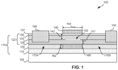
Gallium nitride material transistors and methods associated with the same
PatentInactiveUS7994540B2
Innovation
- The development of gallium nitride material transistors with active regions formed in a gallium nitride layer, integrated with a matching circuit to transform impedance, enabling the amplification of input signals to produce output signals with an adjacent channel power ratio (ACPR) of less than or equal to −20 dBc, while maintaining high drain efficiencies and output powers.
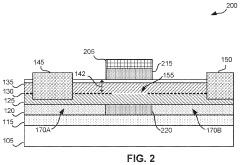
Gallium nitride enhancement mode device
PatentInactiveUS20220093779A1
Innovation
- The fabrication of enhancement mode GaN-based semiconductor devices with a buried p-type region under the two-dimensional electron gas (2DEG) region, allowing for a normally off switching mechanism, achieved by patterning and configuring the p-type material to deplete the 2DEG region and control the threshold voltage, thereby reducing circuit complexity.
Radiation Hardness and Reliability Assessment
Gallium Nitride (GaN) transistors demonstrate exceptional radiation hardness characteristics, making them particularly valuable for aerospace electronics operating in harsh radiation environments. Extensive testing has shown that GaN High Electron Mobility Transistors (HEMTs) maintain functionality after exposure to total ionizing doses exceeding 100 Mrad, significantly outperforming silicon-based alternatives which typically show degradation at much lower radiation levels. This inherent radiation tolerance stems from GaN's wide bandgap (3.4 eV) and strong atomic bonds, which reduce the formation of defects when subjected to high-energy particles.
The reliability assessment of GaN transistors for aerospace applications follows rigorous protocols established by organizations such as NASA, ESA, and the Department of Defense. These assessments typically include accelerated life testing, temperature cycling between extreme values (-55°C to +125°C), and high-temperature operating life tests exceeding 1000 hours. Recent data indicates that properly designed GaN devices can achieve mean time between failures (MTBF) exceeding 10^7 hours at operating temperatures of 150°C, demonstrating exceptional long-term reliability.
Single event effects (SEEs) represent a critical concern for aerospace electronics, as high-energy particles can trigger destructive events in semiconductor devices. GaN transistors exhibit superior resistance to single event burnout (SEB) and single event gate rupture (SEGR) compared to silicon counterparts. Testing with heavy ions having linear energy transfer (LET) values up to 80 MeV-cm²/mg has demonstrated GaN's robustness against these catastrophic failure mechanisms, with threshold voltages for failure significantly higher than those of silicon devices.
The radiation-induced threshold voltage shift in GaN transistors is notably minimal, typically less than 100mV after exposure to 1 Mrad total dose, compared to several volts for conventional silicon MOSFETs. This stability ensures consistent performance in radiation environments encountered during space missions. Furthermore, the leakage current increase post-irradiation remains within acceptable operational parameters, typically less than 10% increase after exposure to radiation levels equivalent to decades in low Earth orbit.
Manufacturing processes significantly impact radiation hardness, with devices fabricated using advanced techniques such as field plates and optimized passivation layers showing enhanced radiation tolerance. Recent developments in GaN-on-Diamond and GaN-on-SiC technologies have further improved thermal management capabilities, addressing a critical reliability concern for high-power aerospace applications. These advancements have extended the operational lifetime of GaN devices under combined thermal and radiation stress conditions.
Qualification standards for aerospace GaN electronics continue to evolve, with the JEDEC JEP001 and MIL-PRF-38535 standards being adapted to address the unique characteristics of wide bandgap semiconductors. Current reliability data suggests that properly qualified GaN transistors can meet or exceed the 15-year operational lifetime requirement for most satellite missions, even in geosynchronous orbits where radiation exposure is significant.
Thermal Management Strategies for GaN in Aerospace
Thermal management represents a critical challenge in the implementation of Gallium Nitride (GaN) transistors for aerospace electronics. The high power density capabilities of GaN devices, while advantageous for performance, generate significant heat that must be effectively dissipated to maintain reliability in the harsh aerospace environment.
Traditional cooling methods such as forced-air convection prove insufficient for GaN applications in aerospace, necessitating more advanced thermal management strategies. Liquid cooling systems have emerged as a promising solution, offering superior heat transfer coefficients compared to air cooling. These systems utilize specialized coolants with high thermal conductivity that can efficiently remove heat from GaN devices while maintaining compatibility with aerospace requirements for weight and reliability.
Advanced thermal interface materials (TIMs) play a crucial role in GaN thermal management. Diamond-based composites and metal matrix composites with thermal conductivities exceeding 1000 W/mK are being deployed to enhance heat transfer from GaN devices to heat sinks. These materials significantly reduce thermal resistance at interfaces, addressing a major bottleneck in thermal dissipation pathways.
Phase change materials (PCMs) represent another innovative approach, particularly valuable for managing transient thermal loads common in aerospace applications. PCMs absorb excess heat during high-power operation and release it during low-power periods, effectively dampening temperature fluctuations that could otherwise compromise GaN device reliability.
Microfluidic cooling technologies have demonstrated exceptional potential for aerospace GaN applications. These systems incorporate microscale channels directly into device packaging or substrates, allowing coolant to flow in close proximity to heat sources. Recent developments in additive manufacturing have enabled complex cooling channel geometries that optimize fluid flow patterns for maximum heat extraction efficiency.
Thermal simulation and modeling tools have become indispensable for aerospace GaN thermal management. Computational fluid dynamics (CFD) coupled with electrothermal models enable accurate prediction of hotspots and thermal gradients under various operating conditions. These simulation capabilities allow engineers to evaluate thermal management strategies virtually before physical implementation, reducing development cycles and costs.
Integration of thermal management with overall system design represents the most holistic approach. This includes strategic placement of GaN devices within aerospace systems, optimization of circuit layouts to distribute heat generation, and coordination with structural elements that can serve dual purposes as heat dissipation pathways.
Unlock deeper insights with PatSnap Eureka Quick Research — get a full tech report to explore trends and direct your research. Try now!
Generate Your Research Report Instantly with AI Agent
Supercharge your innovation with PatSnap Eureka AI Agent Platform!