

How OLED vs MicroLED Influence Semiconductor Efficiency
OCT 23, 20259 MIN READ
Generate Your Research Report Instantly with AI Agent
PatSnap Eureka helps you evaluate technical feasibility & market potential.
OLED and MicroLED Display Technology Evolution
Display technology has undergone significant evolution over the past decades, transitioning from CRT to LCD, and now advancing toward OLED and MicroLED technologies. OLED (Organic Light-Emitting Diode) emerged commercially in the early 2000s, pioneered by companies like Kodak and Sony, offering superior contrast ratios and flexibility compared to traditional displays. The technology matured throughout the 2010s, becoming mainstream in smartphones, televisions, and wearable devices.
MicroLED represents the next frontier in display technology, with roots dating back to the early 2000s when researchers began exploring inorganic LED arrays at microscopic scales. Unlike OLED, which uses organic compounds, MicroLED utilizes inorganic gallium nitride (GaN) materials. Major development milestones occurred around 2012-2014 when companies like Sony and Samsung demonstrated early prototypes, though mass production challenges have delayed widespread commercialization.
The technological trajectory of these display technologies directly impacts semiconductor efficiency. OLED displays initially suffered from manufacturing yield issues and shorter lifespans, particularly for blue pixels. Technological improvements have addressed these concerns through advanced thin-film transistor (TFT) backplanes, more efficient organic materials, and enhanced manufacturing processes like inkjet printing for RGB OLED deposition.
MicroLED technology promises even greater efficiency improvements with its inorganic semiconductor foundation. The evolution path has focused on overcoming mass transfer challenges—moving millions of tiny LED chips precisely onto display substrates. Recent innovations include pick-and-place technologies, laser transfer methods, and fluidic assembly techniques that have gradually improved yield rates and reduced production costs.
Both technologies continue to evolve toward higher energy efficiency, with OLED focusing on reducing power consumption through improved organic materials and driving methods, while MicroLED development concentrates on enhancing quantum efficiency and reducing the size of individual LED elements below 10 micrometers.
The convergence of these display technologies with semiconductor manufacturing has created a symbiotic relationship where advances in one field drive innovation in the other. Semiconductor processes originally developed for computing applications have been adapted for display manufacturing, while unique requirements of display technologies have pushed semiconductor fabrication toward new capabilities in precision, scale, and materials science.
Market Demand Analysis for Advanced Display Technologies
The display technology market is experiencing a significant shift as advanced technologies like OLED and MicroLED continue to evolve. Current market analysis indicates that the global advanced display market reached approximately $143 billion in 2022, with projections suggesting growth to $206 billion by 2027, representing a compound annual growth rate of 7.5%. This growth is primarily driven by increasing consumer demand for higher resolution, energy-efficient displays across multiple sectors including consumer electronics, automotive, and healthcare.
OLED technology currently dominates the premium smartphone and high-end television segments, with Samsung and LG maintaining leadership positions. Market penetration for OLED displays in smartphones has reached nearly 50% in the premium segment, while adoption in television markets continues to grow steadily at 15-20% annually. Consumer preference surveys indicate that 78% of high-end device users prioritize display quality as a critical purchasing factor, directly benefiting OLED technology adoption.
MicroLED, though still emerging, is generating substantial market interest due to its superior brightness, efficiency, and longevity compared to OLED. Market forecasts predict MicroLED will capture 25% of the premium display market by 2028, with initial adoption focused on large-format displays, automotive applications, and augmented reality devices. Investment in MicroLED manufacturing infrastructure has exceeded $4.5 billion over the past three years, signaling strong industry confidence in this technology.
Regional analysis reveals Asia-Pacific continues to lead in both production and consumption of advanced displays, accounting for 65% of global manufacturing capacity. North America and Europe follow with 18% and 12% respectively, primarily focusing on specialized applications and research advancements rather than mass production.
The automotive sector represents the fastest-growing market segment for advanced display technologies, with a projected 22% annual growth rate through 2027. This is driven by increasing integration of digital cockpits, heads-up displays, and entertainment systems in modern vehicles. Consumer electronics remains the largest segment by volume, while healthcare and industrial applications show promising growth trajectories with 18% and 15% annual increases respectively.
Energy efficiency has emerged as a critical market driver, with 82% of enterprise customers citing power consumption as a key consideration in display technology selection. This trend particularly benefits MicroLED technology, which offers 30-40% greater energy efficiency compared to traditional LCD and potential advantages over OLED in certain applications, especially those requiring high brightness and extended operational lifespans.
Current Technical Challenges in Display Semiconductor Efficiency
Despite significant advancements in display technologies, both OLED and MicroLED face substantial technical challenges that impact semiconductor efficiency. OLED displays continue to struggle with differential aging of organic materials, particularly blue emitters which degrade faster than red and green counterparts. This uneven degradation necessitates complex compensation circuits that increase power consumption and reduce overall efficiency of the semiconductor components.
Material stability remains a critical issue, with OLED panels experiencing efficiency degradation over time due to exposure to oxygen and moisture. While encapsulation technologies have improved, they add manufacturing complexity and cost while not completely eliminating the degradation problem, ultimately affecting long-term semiconductor performance.
For MicroLED displays, the primary challenge lies in the mass transfer process of microscopic LED chips. Current pick-and-place technologies struggle to achieve the necessary precision at commercially viable speeds, resulting in yield issues that significantly impact production efficiency. The semiconductor processes required for MicroLED manufacturing demand extremely high precision, with placement accuracy requirements below 1.5 micrometers.
Thermal management presents another significant obstacle for both technologies. OLED displays generate heat during operation that accelerates material degradation, while MicroLED displays face challenges in heat dissipation due to the high density of semiconductor components. This thermal load requires additional power management circuitry that can reduce overall system efficiency.
Power efficiency at low brightness levels remains problematic, particularly for MicroLED. While OLED can achieve pixel-level dimming efficiently, MicroLED struggles with maintaining efficiency at low brightness levels due to the threshold voltage characteristics of inorganic LED semiconductors. This results in disproportionate power consumption at lower brightness settings, a critical consideration for mobile applications.
Color uniformity and consistency present ongoing challenges for both technologies. OLED displays require complex compensation algorithms to maintain uniform brightness and color across the panel as materials age differently. MicroLED faces issues with binning and sorting of LED chips to ensure color consistency, with variations in semiconductor manufacturing processes causing perceptible differences in color output.
Integration density poses a fundamental limitation, particularly for MicroLED. As pixel densities increase for higher resolution displays, the semiconductor architecture must accommodate smaller and more tightly packed components, leading to increased crosstalk, power leakage, and thermal management difficulties that collectively reduce efficiency.
Technical Comparison of OLED vs MicroLED Power Efficiency Solutions
01 OLED efficiency enhancement techniques
Various techniques are employed to enhance the efficiency of OLED displays, including improved electron transport layers, optimized emissive materials, and novel device architectures. These advancements help reduce power consumption while maintaining or improving brightness and color accuracy. Enhanced phosphorescent and fluorescent materials with better quantum efficiency contribute significantly to overall display performance.- OLED efficiency enhancement technologies: Various technologies have been developed to enhance the efficiency of OLED displays. These include improved organic materials, optimized device structures, and novel manufacturing techniques that reduce energy consumption while maintaining or improving display quality. Advanced electrode designs and charge transport layers help balance electron and hole injection, resulting in more efficient light emission and longer device lifetimes.
- MicroLED fabrication and integration methods: MicroLED displays utilize microscopic LED arrays that offer superior brightness, contrast, and energy efficiency compared to traditional display technologies. Advanced fabrication methods include mass transfer techniques for placing tiny LED elements precisely on substrates, integration of driver circuits, and novel bonding approaches. These methods address manufacturing challenges while maintaining the high efficiency that makes MicroLED technology promising for next-generation displays.
- Semiconductor materials for display efficiency: Specialized semiconductor materials play a crucial role in determining the efficiency of both OLED and MicroLED displays. These include advanced quantum dot materials, novel phosphorescent compounds, and engineered semiconductor heterostructures that improve light emission efficiency. Material innovations focus on reducing energy loss pathways, improving charge carrier mobility, and enhancing light extraction to maximize overall display efficiency.
- Power management and driving schemes: Innovative power management systems and driving schemes significantly impact the energy efficiency of OLED and MicroLED displays. These include adaptive brightness control, pixel compensation circuits, and intelligent power distribution systems that optimize energy usage based on displayed content. Advanced driving methods reduce power consumption during operation while maintaining image quality and extending battery life in portable devices.
- Thermal management for display efficiency: Effective thermal management is essential for maintaining the efficiency of both OLED and MicroLED displays. Heat dissipation techniques, including specialized substrate materials, thermal interface materials, and cooling structures, help prevent efficiency degradation at high brightness levels. By controlling operating temperatures, these solutions extend device lifetime, maintain consistent color performance, and allow displays to operate at peak efficiency levels for longer periods.
02 MicroLED fabrication and integration methods
MicroLED displays utilize innovative fabrication and integration methods to achieve high efficiency. These include advanced transfer techniques for placing microscopic LED elements onto display substrates, improved semiconductor structures, and novel bonding methods. The miniaturization of LED components while maintaining high light output efficiency represents a significant advancement in display technology.Expand Specific Solutions03 Power management and thermal efficiency
Power management systems and thermal efficiency solutions are critical for both OLED and MicroLED technologies. These include adaptive brightness control, efficient driving circuits, and heat dissipation structures. Improved power management not only extends battery life in portable devices but also enhances the longevity of display components by reducing thermal stress and preventing degradation.Expand Specific Solutions04 Quantum dot integration for color enhancement
Quantum dot technology is being integrated with both OLED and MicroLED displays to enhance color gamut and efficiency. These semiconductor nanocrystals can convert light with high efficiency and provide precise color control. The integration of quantum dots allows for improved color accuracy, wider color gamut, and potentially reduced power consumption in display applications.Expand Specific Solutions05 Novel semiconductor materials for display efficiency
Research into novel semiconductor materials is advancing the efficiency of both OLED and MicroLED displays. These materials include improved organic compounds for OLEDs and advanced III-V semiconductors for MicroLEDs. Material innovations focus on enhancing electron mobility, improving quantum efficiency, and extending operational lifetime while maintaining high brightness and color purity.Expand Specific Solutions
Key Industry Players in Display Semiconductor Manufacturing
The OLED vs MicroLED competition in semiconductor efficiency is evolving through distinct market phases. Currently in a transition stage, the OLED market is mature with established players like Samsung Display, LG Display, and BOE Technology dominating production, while MicroLED remains in early commercialization with companies like Samsung Electronics, Apple, and emerging specialists like eLux and X Display Co. developing innovative solutions. The global display market is projected to reach $200 billion by 2025, with MicroLED expected to capture increasing share due to superior efficiency and longevity. Technologically, OLED has reached commercial maturity while MicroLED faces manufacturing challenges, particularly in mass transfer techniques, with companies like Applied Materials and Lumileds working on semiconductor process improvements to enhance efficiency and reduce production costs.
BOE Technology Group Co., Ltd.
Technical Solution: BOE has made significant advancements in both OLED and MicroLED semiconductor technologies with a focus on efficiency optimization. For OLED displays, BOE has developed flexible AMOLED technology utilizing low-temperature polycrystalline oxide (LTPO) backplanes that enable variable refresh rates from 1Hz to 120Hz, reducing power consumption by up to 30% compared to fixed refresh rate displays. Their semiconductor integration includes proprietary pixel compensation circuits that maintain uniform current distribution across the display, improving overall efficiency by minimizing hotspots that waste energy. BOE's OLED pixel architecture incorporates advanced thin film encapsulation (TFE) technology that reduces the number of layers while maintaining barrier performance, allowing for better light extraction efficiency. For MicroLED development, BOE has created a novel "chip-on-glass" integration approach that directly bonds microLED chips to the glass substrate with integrated circuits, reducing connection resistance and improving thermal management. Their semiconductor design includes specialized driver ICs that implement adaptive current control algorithms, dynamically adjusting power delivery based on image content to achieve up to 25% energy savings compared to static driving methods. BOE has also pioneered hybrid semiconductor materials for MicroLED, combining traditional III-V compounds with silicon-based technologies to optimize the balance between light emission efficiency and manufacturing scalability.
Strengths: BOE's vertical integration capabilities allow for customized semiconductor solutions optimized specifically for display efficiency. Their massive production scale enables rapid iteration and improvement of manufacturing processes. Weaknesses: Their MicroLED technology still faces yield challenges at mass production scales, increasing costs. Their OLED technology shows slightly lower color volume and peak brightness efficiency compared to industry leaders.
Samsung Electronics Co., Ltd.
Technical Solution: Samsung has pioneered both OLED and MicroLED technologies with significant advancements in semiconductor efficiency. For OLED, Samsung utilizes thin-film transistor (TFT) backplanes with low-temperature polysilicon (LTPS) technology that enables higher electron mobility (100 cm²/Vs compared to a-Si's 0.5-1 cm²/Vs), resulting in more efficient current delivery to organic materials. Their quantum dot (QD)-OLED hybrid technology further improves energy efficiency by approximately 25% compared to conventional OLED displays. For MicroLED, Samsung has developed proprietary mass transfer techniques that allow placement of microscopic RGB LED chips (under 50 micrometers) with precision at scale. Their MicroLED architecture eliminates the need for color filters and polarizers, achieving nearly 100% light utilization efficiency compared to OLED's typical 20-40% light extraction efficiency. Samsung's semiconductor integration includes advanced driver ICs that optimize power management across different brightness levels, reducing overall system power consumption by up to 30% in their latest display generations.
Strengths: Samsung's vertical integration allows for optimized semiconductor components specifically designed for their display technologies, resulting in better power efficiency. Their extensive manufacturing experience enables high-yield production of both technologies at scale. Weaknesses: MicroLED production costs remain significantly higher than OLED, limiting mass market adoption. Their OLED technology still faces challenges with blue pixel degradation affecting long-term efficiency.
Critical Patents and Innovations in Display Semiconductor Materials
Display substrate, display device, and control method thereof
PatentActiveUS20210183311A1
Innovation
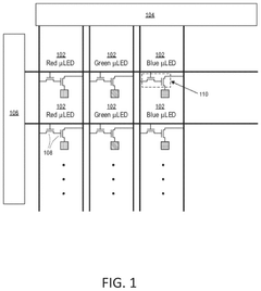
- A display substrate with a configuration of multiple sub-pixels, including a fourth sub-pixel with the same emission color as the first sub-pixel, where the light emission is controlled based on ambient temperature to compensate for brightness changes, reducing color cast by adjusting the emission of sub-pixels accordingly.


Semiconductor smoothing apparatus and method
PatentActiveUS12119435B2
Innovation
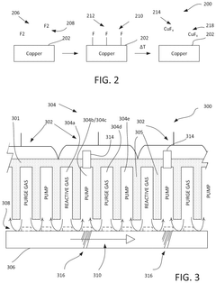
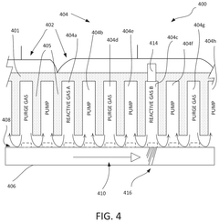
- A semiconductor manufacturing apparatus with discrete open chambers is used to smooth copper surfaces on large substrates, employing reactive plasma or ionic gases to form volatile compounds that are then vaporized and removed, followed by purging, to achieve atomic-level smoothness of copper contact pads, enabling effective bonding between micro-LED elements and the display backplane.
Supply Chain Considerations for Next-Generation Display Technologies
The global display technology supply chain is undergoing significant transformation as OLED and MicroLED technologies compete for market dominance. These advanced display technologies require fundamentally different semiconductor materials and manufacturing processes, creating distinct supply chain architectures with varying implications for efficiency and sustainability.
OLED supply chains are currently more mature, centered around organic materials production facilities primarily located in South Korea, Japan, and increasingly China. Key suppliers include Universal Display Corporation for phosphorescent materials and companies like Merck and DuPont for other critical organic compounds. The semiconductor components for OLED driver circuits rely on established silicon foundries, with Samsung and LG Display vertically integrating much of their supply chain to optimize efficiency.
MicroLED supply chains, by contrast, remain nascent and fragmented. The technology demands specialized LED manufacturing capabilities using gallium nitride (GaN) on various substrates. Current bottlenecks include mass transfer technologies for placing millions of microscopic LEDs precisely onto display substrates. Companies like Apple, Samsung, and Sony have been securing strategic partnerships with specialized LED manufacturers and investing in proprietary mass transfer technologies to overcome these challenges.
From a semiconductor efficiency perspective, the supply chain differences are substantial. OLED production benefits from economies of scale but suffers from material waste during vapor deposition processes. MicroLED manufacturing currently experiences lower yield rates during the critical mass transfer stage, though theoretical material efficiency could eventually surpass OLED once manufacturing processes mature.
Regional dependencies also differ significantly between these technologies. OLED supply chains are heavily concentrated in East Asia, while MicroLED may enable more geographically distributed manufacturing due to its compatibility with existing semiconductor facilities in Europe and North America. This could reduce transportation-related carbon emissions and supply chain vulnerabilities.
Energy consumption throughout the supply chain represents another critical efficiency consideration. OLED manufacturing requires less energy-intensive processes compared to MicroLED, which needs high-temperature epitaxial growth for LED creation. However, the longer operational lifespan of MicroLED displays may offset these initial energy investments when considering lifecycle efficiency.
Raw material sourcing presents contrasting challenges: OLED relies on specialized organic compounds with limited suppliers, while MicroLED depends on rare earth elements and semiconductor materials with established but potentially vulnerable supply chains. Diversification strategies are emerging in both sectors to mitigate these risks and improve overall supply chain resilience.
Environmental Impact and Sustainability of Display Manufacturing Processes
The manufacturing processes of display technologies have significant environmental implications, with OLED and MicroLED presenting distinct sustainability profiles that directly impact semiconductor efficiency. OLED production typically involves vacuum thermal evaporation processes that consume substantial energy, particularly during the deposition of organic materials. These processes generate considerable waste and often utilize rare materials with limited global supplies, raising concerns about resource depletion.
In contrast, MicroLED manufacturing employs different semiconductor fabrication techniques that may offer improved environmental efficiency. The production process for MicroLED displays involves epitaxial growth of LED structures on semiconductor wafers, which can be optimized for higher material utilization rates compared to OLED manufacturing. This potentially reduces waste generation per unit of display area produced.
Energy consumption patterns differ significantly between these technologies. OLED manufacturing facilities typically require extensive clean room environments with precise temperature and humidity controls, contributing to their substantial energy footprint. MicroLED production, while also demanding clean room conditions, may achieve better energy efficiency ratios when considering the semiconductor processing steps involved, particularly as manufacturing scales increase and processes mature.
Water usage represents another critical environmental factor. OLED manufacturing requires extensive cleaning processes that consume large volumes of ultra-pure water. MicroLED production similarly demands significant water resources, though emerging innovations in semiconductor manufacturing are beginning to implement water recycling systems that could reduce the overall environmental impact of display production.
Chemical usage and hazardous waste generation remain challenging aspects of both technologies. OLED production involves numerous organic solvents and potentially toxic materials, while MicroLED manufacturing utilizes various etching chemicals and semiconductor dopants. The semiconductor efficiency of both technologies is directly influenced by how effectively these materials are utilized and processed, with implications for both environmental impact and production costs.
End-of-life considerations further differentiate these display technologies. OLED displays contain organic materials that may present recycling challenges, whereas MicroLED components might offer better potential for material recovery due to their inorganic semiconductor composition. This recyclability factor increasingly influences the full lifecycle assessment of semiconductor efficiency in modern display technologies.
As industry sustainability standards evolve, manufacturers are developing innovative approaches to reduce environmental footprints while maintaining semiconductor efficiency. These include closed-loop manufacturing systems, renewable energy integration, and advanced material recovery techniques that promise to reshape the environmental profile of next-generation display technologies.
Unlock deeper insights with PatSnap Eureka Quick Research — get a full tech report to explore trends and direct your research. Try now!
Generate Your Research Report Instantly with AI Agent
Supercharge your innovation with PatSnap Eureka AI Agent Platform!