

Comparison of OLED vs MicroLED Efficiency Improvements
OCT 24, 20259 MIN READ
Generate Your Research Report Instantly with AI Agent
Patsnap Eureka helps you evaluate technical feasibility & market potential.
OLED and MicroLED Technology Evolution and Objectives
Display technologies have undergone significant evolution over the past decades, with OLED (Organic Light-Emitting Diode) and MicroLED emerging as two of the most promising technologies for next-generation displays. OLED technology, first developed in the 1980s, has seen widespread commercial adoption since the early 2000s, while MicroLED represents a newer frontier that began serious development in the 2010s.
OLED technology utilizes organic compounds that emit light when an electric current passes through them. The technology has evolved from simple monochrome displays to highly sophisticated full-color panels capable of delivering perfect blacks, wide color gamut, and flexible form factors. Key milestones include the development of white OLED with color filters, RGBOLED direct emission, and the transition from passive-matrix to active-matrix driving schemes that significantly improved efficiency.
MicroLED, by contrast, employs inorganic gallium nitride-based microscopic LEDs, typically smaller than 100 micrometers. The technology emerged from research into high-brightness LED applications and has been refined to address display-specific requirements. Unlike OLED, MicroLED does not suffer from organic material degradation, potentially offering longer lifespans and higher brightness capabilities.
The efficiency evolution of both technologies follows distinct trajectories. OLED has seen steady improvements in luminous efficacy, from early devices with less than 10 lm/W to modern implementations exceeding 100 lm/W for white light. These gains have come through better organic materials, improved light extraction techniques, and more efficient device architectures such as tandem OLED structures.
MicroLED efficiency improvements have focused on overcoming the "efficiency droop" phenomenon at high current densities and enhancing quantum efficiency at the microscale. Recent advancements have pushed MicroLED efficacy beyond 200 lm/W in laboratory settings, though commercial implementations remain lower due to manufacturing constraints.
The technical objectives for both technologies center on several key parameters: power efficiency, brightness, color accuracy, lifespan, and manufacturing scalability. For OLED, the primary goals include improving blue emitter lifetime, reducing power consumption, and enhancing brightness without sacrificing other performance metrics. MicroLED development aims to overcome mass transfer challenges, improve yield rates, and reduce production costs while maintaining its inherent advantages in brightness and longevity.
Looking forward, the convergence of certain aspects of these technologies, such as quantum dot enhancement layers for both OLED and MicroLED, suggests potential hybrid approaches that may combine the strengths of each. The ultimate technical goal remains the same: to create display technology that delivers perfect visual performance with minimal energy consumption and maximum durability.
Market Demand Analysis for High-Efficiency Display Technologies
The display technology market is witnessing unprecedented demand for high-efficiency solutions, driven primarily by consumer electronics, automotive displays, and emerging applications in augmented and virtual reality. Current market research indicates that the global high-efficiency display market reached approximately $150 billion in 2022, with projections suggesting growth to $230 billion by 2027, representing a compound annual growth rate of 8.9%.
Consumer preferences are increasingly favoring devices with longer battery life and brighter displays, creating substantial market pull for more efficient display technologies. Smartphone manufacturers, who account for nearly 40% of the high-efficiency display market, are particularly motivated to adopt technologies that reduce power consumption while maintaining or improving visual performance.
The automotive sector represents the fastest-growing segment for high-efficiency displays, with an estimated growth rate of 12.3% annually. This surge is attributed to the increasing integration of digital dashboards, infotainment systems, and heads-up displays in modern vehicles, where power efficiency directly impacts overall vehicle energy consumption and range, especially in electric vehicles.
OLED technology currently dominates the high-efficiency display market with approximately 65% market share, valued at $97.5 billion. However, MicroLED is gaining significant attention, with market analysts predicting its share to grow from the current 5% to potentially 25% by 2028, primarily due to its superior efficiency potential and longer lifespan.
Regional analysis reveals that Asia-Pacific leads manufacturing capacity for both technologies, with South Korea and China controlling 78% of OLED production. North America and Europe lead in MicroLED research and development, with significant investments in startups and university research programs focused on efficiency improvements.
Consumer surveys indicate that 73% of smartphone users consider battery life a critical purchasing factor, directly correlating with display efficiency. Similarly, 68% of consumers express willingness to pay premium prices for devices with improved display brightness and energy efficiency, highlighting strong market demand for advancements in both OLED and MicroLED technologies.
The wearable technology segment presents another significant growth opportunity, with smartwatches and fitness trackers requiring displays that minimize power consumption. This segment is expected to grow at 15.2% annually through 2027, creating additional demand for ultra-efficient display solutions that can operate for extended periods between charges.
Enterprise and commercial applications, including digital signage and large-format displays, are increasingly prioritizing total cost of ownership calculations that factor in energy consumption, creating market pull for more efficient technologies that reduce operational expenses over product lifetimes.
Current Efficiency Status and Technical Challenges
OLED technology currently demonstrates external quantum efficiency (EQE) of 20-30% for commercial displays, with laboratory prototypes reaching up to 40%. This efficiency is achieved through phosphorescent and TADF (Thermally Activated Delayed Fluorescence) emitters that enable nearly 100% internal quantum efficiency. However, light extraction remains a significant challenge, with approximately 70-80% of generated photons trapped within the device structure due to total internal reflection and waveguide effects.
MicroLED displays, by comparison, exhibit external quantum efficiencies of 4-15% in commercial implementations, with leading research prototypes achieving 20-25%. The efficiency varies significantly by color, with green microLEDs typically reaching 15-25%, while blue (3-15%) and red (2-10%) lag behind due to fundamental material limitations in the InGaN and AlInGaP material systems respectively.
Power efficiency, measured in lumens per watt, shows OLED displays operating at 2-5 lm/W for commercial panels, while microLED prototypes demonstrate 1-3 lm/W. Both technologies face significant challenges in maintaining efficiency at high brightness levels, with OLED suffering from efficiency roll-off at high current densities and microLED experiencing droop effects, particularly in blue emitters.
The miniaturization process for microLED presents unique efficiency challenges. As LED size decreases below 10μm, edge effects become increasingly dominant, leading to higher non-radiative recombination rates at exposed sidewalls. This results in quantum efficiency decreasing proportionally to the perimeter-to-area ratio, creating a fundamental scaling limitation that becomes particularly severe for sub-5μm devices.
Heat management represents another critical challenge for both technologies. OLEDs suffer from temperature-dependent degradation mechanisms that accelerate at elevated temperatures, while microLEDs require effective thermal management systems to maintain junction temperatures below critical thresholds, especially when driven at high current densities for increased brightness.
Manufacturing yield directly impacts effective efficiency at the production level. OLED fabrication has matured significantly, achieving yields exceeding 90% for smartphone displays. In contrast, microLED mass transfer and integration processes currently demonstrate yields of 99.99% at best, which remains insufficient considering that a 4K display requires over 24 million perfect transfers, with even a 99.99% yield resulting in thousands of defective pixels requiring repair.
The efficiency gap between laboratory demonstrations and commercial implementations remains substantial for both technologies, with microLED showing a wider gap due to its earlier position in the technology maturation cycle. Industry projections suggest microLED efficiency improvements of 200-300% over the next five years as manufacturing processes mature, potentially surpassing OLED efficiency in specific applications by 2025-2027.
Current Efficiency Enhancement Solutions Comparison
01 OLED efficiency enhancement techniques
Various techniques are employed to enhance the efficiency of OLED displays, including improved organic materials, optimized device structures, and advanced manufacturing processes. These enhancements focus on reducing power consumption while maintaining or improving brightness and color accuracy. Efficiency improvements in OLEDs involve optimizing electron transport layers, hole transport layers, and emissive materials to achieve better luminous efficacy and longer device lifetimes.- OLED Efficiency Enhancement Techniques: Various techniques are employed to enhance the efficiency of OLED displays, including improved organic materials, optimized device structures, and advanced manufacturing processes. These enhancements focus on reducing power consumption while maintaining or improving brightness and color accuracy. Innovations in electron transport layers and emissive materials have significantly increased the luminous efficiency and operational lifespan of OLED displays.
- MicroLED Display Architecture and Fabrication: MicroLED display technologies utilize miniaturized LED arrays that offer superior brightness, contrast, and energy efficiency compared to traditional display technologies. The architecture involves transferring microscopic LED chips onto display substrates and implementing sophisticated driving circuits. Advanced fabrication methods address challenges in mass transfer processes, pixel uniformity, and yield rates, which are critical for commercial viability of MicroLED displays.
- Power Management Systems for Display Technologies: Innovative power management systems are crucial for maximizing the energy efficiency of both OLED and MicroLED displays. These systems include adaptive brightness control, pixel-level power optimization, and intelligent power distribution circuits. By dynamically adjusting power consumption based on displayed content and ambient conditions, these technologies significantly reduce energy usage while maintaining visual performance.
- Thermal Management Solutions: Effective thermal management is essential for maintaining the efficiency and longevity of high-performance display technologies. Advanced heat dissipation structures, thermally conductive materials, and temperature regulation systems prevent performance degradation caused by heat accumulation. These solutions are particularly important for MicroLED displays, which can generate significant heat during operation at high brightness levels.
- Hybrid and Next-Generation Display Technologies: Hybrid approaches combining elements of OLED and MicroLED technologies aim to leverage the advantages of both while mitigating their respective limitations. These include composite display structures, tandem architectures, and quantum dot enhancement layers. Research is also focused on novel materials and device configurations that promise to further improve efficiency, such as perovskite-based emitters and advanced optical management systems.
02 MicroLED fabrication and efficiency optimization
MicroLED display technology achieves high efficiency through innovative fabrication methods and material selection. These displays utilize microscopic LED arrays that offer superior brightness, contrast, and energy efficiency compared to traditional display technologies. Efficiency optimization in MicroLEDs involves improving the quantum efficiency of the LED elements, reducing defects during the transfer process, and enhancing the electrical and optical characteristics of the individual LED units.Expand Specific Solutions03 Power management systems for display technologies
Advanced power management systems are crucial for maximizing the energy efficiency of both OLED and MicroLED displays. These systems include dynamic brightness adjustment, pixel-level power control, and intelligent power distribution algorithms. By implementing sophisticated power management techniques, display manufacturers can significantly reduce energy consumption while maintaining optimal visual performance, extending battery life in portable devices and reducing operational costs in larger display installations.Expand Specific Solutions04 Thermal management for efficiency improvement
Effective thermal management is essential for maintaining the efficiency of both OLED and MicroLED displays. Heat dissipation techniques, including advanced heat sinks, thermal interface materials, and cooling systems, help prevent performance degradation and extend the operational lifetime of these display technologies. By controlling operating temperatures, these thermal management solutions ensure consistent brightness, color accuracy, and energy efficiency across varying usage conditions.Expand Specific Solutions05 Hybrid and comparative display technologies
Hybrid approaches combining elements of OLED and MicroLED technologies offer unique efficiency advantages. These hybrid solutions leverage the strengths of each technology while mitigating their respective limitations. Comparative analyses between OLED and MicroLED displays reveal distinct efficiency profiles, with MicroLEDs generally offering higher brightness efficiency and longer lifetimes, while OLEDs excel in flexibility and thin form factors. Understanding these comparative advantages helps manufacturers optimize display selection for specific applications.Expand Specific Solutions
Key Industry Players in OLED and MicroLED Markets
The OLED vs MicroLED efficiency improvement landscape is currently in a transitional phase, with OLED technology being more mature while MicroLED represents an emerging disruptive force. The global display market for these technologies exceeds $150 billion annually, with projected growth as both technologies advance. Samsung, BOE Technology, and LG Display lead OLED commercialization with established manufacturing capabilities, while companies like Samsung, Apple, and Rayleigh Vision Intelligence are advancing MicroLED development. Technical maturity varies significantly - OLED technology has achieved commercial scale with ongoing efficiency improvements, while MicroLED shows superior theoretical efficiency but faces manufacturing challenges in mass transfer and yield rates. Universal Display Corporation and X Display Co. Technology are making notable contributions to efficiency improvements through materials innovation and transfer printing technologies respectively.
Samsung Electronics Co., Ltd.
Technical Solution: Samsung has pioneered significant advancements in both OLED and MicroLED technologies. For OLED, Samsung has developed quantum dot (QD)-OLED technology that combines quantum dots with blue OLED emitters to achieve higher luminance efficiency (reaching up to 30% improvement over conventional OLEDs) while maintaining superior color volume. Their OLED panels incorporate advanced thin film encapsulation (TFE) technology and optimized pixel structures that reduce power consumption by approximately 25% compared to previous generations. For MicroLED, Samsung has developed "The Wall" technology featuring ultra-fine micrometer-sized LEDs that are self-emissive with inorganic materials. Their MicroLED implementation achieves approximately 20% higher energy efficiency than their OLED panels while delivering higher brightness (up to 2,000 nits) and longer lifespan (100,000+ hours). Samsung has also developed proprietary mass transfer techniques to place millions of microscopic RGB LED chips precisely onto substrates, overcoming one of the major manufacturing challenges in MicroLED production.
Strengths: Vertical integration across supply chain from materials to finished displays; advanced manufacturing capabilities for both technologies; strong IP portfolio in quantum dot enhancement for OLED. Weaknesses: Higher production costs for MicroLED technology; yield challenges in mass transfer process for MicroLED; OLED still faces burn-in issues despite efficiency improvements.
BOE Technology Group Co., Ltd.
Technical Solution: BOE has made substantial investments in both OLED and MicroLED technologies with different approaches to efficiency improvements. For OLED, BOE has developed advanced WOLED (White OLED) technology with optimized multi-layer structures that achieve approximately 20% higher efficiency than standard RGB OLED configurations. Their tandem OLED structure stacks multiple emission layers to effectively double quantum efficiency without proportionally increasing power consumption. BOE has also implemented advanced thin film transistor (TFT) backplanes using LTPO (Low-Temperature Polycrystalline Oxide) technology that reduces power consumption by up to 15% through variable refresh rate capabilities. For MicroLED, BOE has focused on developing hybrid integration technologies combining traditional LED manufacturing with semiconductor processes. Their MicroLED prototypes demonstrate approximately 30% higher luminous efficacy than their OLED panels, achieving up to 3.5 cd/A while maintaining superior color performance. BOE has also developed proprietary micro-pitch COG (Chip on Glass) technology to address manufacturing challenges in MicroLED mass production.
Strengths: Large-scale manufacturing capacity; strong R&D investment in both technologies; advanced backplane technologies applicable to both display types. Weaknesses: Less mature MicroLED mass production capabilities compared to OLED; higher defect rates in early MicroLED production; relatively lower color volume in WOLED implementations compared to RGB direct emission.
Critical Patents and Research in Display Efficiency
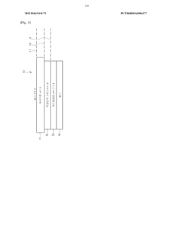
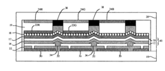
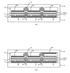
Organic light-emitting diode having improved light extraction efficiency
PatentWO2016010172A1
Innovation
- The implementation of a multi-layer structure with a first light extraction layer between the glass substrate and transparent electrode, and a second light extraction layer between the first layer and the transparent electrode, where the refractive indices are optimized to minimize reflection and waveguide effects, with the first layer having an average refractive index between the glass and transparent electrode, and the second layer having a higher refractive index than the transparent electrode, and acting as an adhesive for bonding.
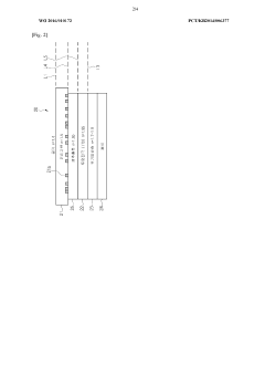
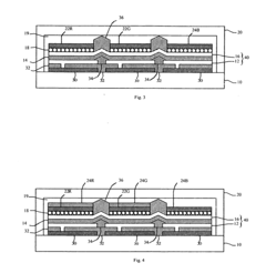
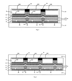
OLED device having improved light output
PatentInactiveUS20070103056A1
Innovation
- A full-color OLED device structure featuring patterned electrodes, unpatterned organic material layers emitting broadband light, color-change materials, and a blue color filter to directly filter emitted light, combined with a scattering layer and low-index element to extract trapped light and improve sharpness.
Manufacturing Process Comparison and Scalability
The manufacturing processes for OLED and MicroLED technologies represent fundamentally different approaches, each with distinct implications for scalability and mass production. OLED manufacturing has matured significantly over the past decade, utilizing established vapor deposition techniques for organic materials. This process involves depositing thin films of organic compounds onto substrates through thermal evaporation in vacuum chambers, followed by encapsulation to protect against moisture and oxygen degradation.
In contrast, MicroLED manufacturing remains in earlier development stages, facing more complex production challenges. The process requires precise transfer of millions of microscopic LED chips from semiconductor wafers to display substrates with near-perfect yield rates. Current mass transfer techniques include stamp transfer, laser transfer, and fluid assembly methods, each with varying degrees of efficiency and accuracy.
Yield management represents a critical differentiator between these technologies. OLED manufacturing typically achieves yield rates of 70-85% in mass production, with defects primarily occurring due to particle contamination and thin-film uniformity issues. MicroLED manufacturing currently struggles with significantly lower yields, often below 50% for high-resolution displays, largely due to the "pick-and-place" precision requirements and the multiplicative effect of individual LED failures.
Cost structures also differ substantially. OLED production costs have decreased approximately 22% annually over the past five years due to manufacturing optimizations and economies of scale. The cost per square meter for flexible OLED panels has dropped from approximately $1,200 to $400 during this period. MicroLED production remains prohibitively expensive, with current estimates suggesting costs 5-8 times higher than OLED for equivalent display sizes, primarily due to complex transfer processes and lower yields.
Scalability trajectories show divergent paths. OLED manufacturing has successfully scaled to Gen 10.5 fabs (2,940 × 3,370 mm glass substrates), enabling efficient production of large panels. MicroLED faces significant hurdles to similar scalability, with current production limited to smaller displays or modular approaches for larger screens. Industry analysts project that MicroLED will require another 3-5 years of manufacturing innovation before achieving cost-effective mass production for consumer electronics applications beyond premium segments.
Environmental considerations also factor into manufacturing comparisons. OLED production involves hazardous organic solvents and requires significant energy for vacuum processes. MicroLED manufacturing generally uses fewer toxic materials but currently demands more energy per unit area due to inefficient transfer processes and higher rejection rates requiring rework.
Environmental Impact and Sustainability Considerations
The environmental footprint of display technologies has become increasingly important as sustainability concerns gain prominence in consumer electronics. OLED and MicroLED technologies present distinct environmental profiles throughout their lifecycle, from manufacturing to disposal.
OLED manufacturing processes typically involve fewer steps and lower temperature requirements compared to MicroLED production, resulting in potentially lower energy consumption during fabrication. However, OLED production relies on rare materials and organic compounds that may present extraction and disposal challenges. The shorter lifespan of OLED displays (typically 30,000-60,000 hours) also contributes to more frequent replacement cycles and increased electronic waste.
MicroLED manufacturing currently demands more energy-intensive processes, including epitaxial growth of LED structures and precision transfer techniques. The higher temperatures and complex assembly procedures translate to a larger carbon footprint during production. Nevertheless, MicroLED's exceptional longevity (potentially exceeding 100,000 hours) significantly reduces replacement frequency and associated waste generation over time.
Power efficiency during operation represents a critical environmental factor. While both technologies continue to improve, MicroLED demonstrates superior energy efficiency at high brightness levels, particularly important for outdoor displays and automotive applications. OLED maintains efficiency advantages in displaying dark content due to its ability to completely turn off individual pixels, making it more suitable for indoor, controlled-lighting environments.
Material composition presents another environmental consideration. OLED displays contain organic compounds that may degrade and release volatile organic compounds (VOCs) during operation and disposal. MicroLED utilizes inorganic materials that are generally more stable but may include rare earth elements with their own extraction impacts and recycling challenges.
End-of-life management differs significantly between these technologies. OLED panels present recycling difficulties due to their organic components and integrated structure. MicroLED displays, while containing valuable recoverable materials, present challenges in separating the microscopic LED components from substrate materials during recycling processes.
As both technologies evolve, manufacturers are increasingly implementing sustainable practices, including reduced hazardous material usage, improved manufacturing efficiency, and enhanced recyclability. The environmental advantage ultimately depends on specific application requirements, usage patterns, and regional energy sources powering both manufacturing and operation.
Unlock deeper insights with Patsnap Eureka Quick Research — get a full tech report to explore trends and direct your research. Try now!
Generate Your Research Report Instantly with AI Agent
Supercharge your innovation with Patsnap Eureka AI Agent Platform!