

OLED vs MicroLED: Standards Impacting Innovation
OCT 24, 20259 MIN READ
Generate Your Research Report Instantly with AI Agent
Patsnap Eureka helps you evaluate technical feasibility & market potential.
OLED and MicroLED Technology Evolution and Objectives
Display technology has undergone significant evolution since the introduction of cathode ray tubes (CRTs) in the early 20th century. The transition from CRTs to liquid crystal displays (LCDs) marked the first major shift toward flatter, more energy-efficient screens. OLED (Organic Light-Emitting Diode) technology emerged in the late 1980s, with the first commercial applications appearing in the early 2000s, revolutionizing display technology with its self-emissive properties, eliminating the need for backlighting.
OLED displays offer superior contrast ratios, wider viewing angles, and faster response times compared to traditional LCD technology. The organic compounds in OLEDs emit light when an electric current passes through them, allowing for thinner, more flexible displays with deeper blacks and more vibrant colors. This technology has become dominant in high-end smartphones, televisions, and wearable devices due to these advantages.
MicroLED represents the next evolutionary step in display technology, addressing some limitations of OLED. Developed in the early 2000s but only recently approaching commercial viability, MicroLED utilizes inorganic gallium nitride-based LEDs that are microscopic in size—typically less than 100 micrometers. Unlike OLEDs, MicroLEDs use inorganic materials that offer longer lifespans, higher brightness levels, and improved energy efficiency.
The technical evolution trajectory shows a clear trend toward displays with higher resolution, better color accuracy, lower power consumption, and increased durability. Both OLED and MicroLED technologies align with this trajectory but represent different approaches to achieving these goals. OLED has matured significantly, while MicroLED remains in earlier commercialization stages with substantial growth potential.
Current technical objectives for OLED development include addressing burn-in issues, improving blue OLED lifespan, enhancing manufacturing yields, and reducing production costs. For MicroLED, the primary objectives involve overcoming mass production challenges, particularly in the transfer process of millions of microscopic LEDs, reducing defect rates, and achieving cost-effective manufacturing at scale.
The industry is also pursuing convergent objectives for both technologies: achieving higher pixel densities for applications like AR/VR headsets, developing more energy-efficient displays for mobile devices, improving color gamut coverage, and creating truly flexible or rollable displays. Standards development organizations are working to establish specifications that will guide innovation while ensuring interoperability across devices and platforms.
As these technologies continue to evolve, we anticipate a period of coexistence where OLED dominates certain market segments while MicroLED gradually gains traction in premium applications before potentially achieving broader market penetration as manufacturing challenges are resolved.
Market Demand Analysis for Advanced Display Technologies
The display technology market is witnessing a significant shift in demand patterns as consumers and industries increasingly prioritize superior visual experiences across devices. OLED (Organic Light Emitting Diode) technology has established a strong market presence over the past decade, capturing substantial market share in premium smartphones, high-end televisions, and wearable devices. Industry reports indicate the global OLED market reached approximately $38 billion in 2022, with projections suggesting continued growth at a compound annual growth rate of 13.4% through 2028.
Meanwhile, MicroLED technology represents an emerging disruptive force in the display market. Though currently in earlier commercialization stages, market research indicates rapidly accelerating demand, particularly in premium segments where performance advantages justify higher price points. The global MicroLED market, while smaller at present, is projected to grow at an exceptional rate of over 80% annually through 2026, reflecting the technology's promising potential.
Consumer electronics remains the primary demand driver for both technologies, with smartphones accounting for over 40% of OLED panel shipments. Television manufacturers are increasingly adopting both technologies for premium models, with OLED currently dominating but MicroLED gaining traction in ultra-high-end segments. The automotive industry represents a particularly promising growth sector, with advanced display technologies increasingly integrated into vehicle dashboards, entertainment systems, and heads-up displays.
Regional analysis reveals Asia-Pacific as the dominant manufacturing hub, while North America and Europe lead in technology adoption for premium applications. China has emerged as both a major producer and consumer market, with domestic manufacturers rapidly expanding production capacity for both technologies.
Key market demand factors include increasing consumer preference for thinner, lighter devices with superior visual quality and energy efficiency. Commercial applications prioritize durability, brightness, and longevity—areas where MicroLED potentially offers advantages over OLED. The gaming and virtual reality sectors represent specialized high-growth segments demanding responsive displays with minimal motion blur and latency.
Price sensitivity remains a critical market factor, with MicroLED's higher production costs currently limiting mass-market adoption. However, industry analysts project manufacturing economies of scale will gradually reduce this gap, potentially accelerating market penetration as production techniques mature and standardization increases.
The COVID-19 pandemic accelerated certain market trends, including increased demand for home entertainment systems and professional displays for remote work environments. This shift has created additional momentum for premium display technologies, with consumers demonstrating willingness to invest in superior visual experiences for both work and entertainment applications.
Current Technical Challenges in OLED and MicroLED Development
Despite significant advancements in display technologies, both OLED and MicroLED face substantial technical challenges that impede their widespread adoption and further innovation. These challenges represent critical barriers that industry standards must address to facilitate technological progress.
OLED technology continues to struggle with limited lifetime issues, particularly for blue emitters which degrade faster than red and green counterparts. This differential aging leads to color shift over time, compromising display quality. The organic materials' susceptibility to moisture and oxygen necessitates complex encapsulation solutions, increasing manufacturing complexity and costs. Additionally, OLED displays suffer from burn-in problems when static images are displayed for extended periods, limiting their application in certain professional environments.
Manufacturing scalability remains a significant hurdle for OLED, particularly for larger displays. Current vapor deposition processes used for small molecule OLEDs face efficiency challenges when scaled to larger substrates, while solution-processed OLEDs struggle to achieve comparable performance and uniformity. These limitations have restricted OLED's penetration into certain market segments, particularly large-format displays.
MicroLED technology faces even more formidable manufacturing challenges. The mass transfer process—moving millions of tiny LED chips from growth substrates to display substrates with perfect precision—remains the most significant technical barrier. Current pick-and-place methods are too slow for commercial viability, while alternative approaches like laser transfer and fluid assembly lack the necessary precision and yield rates.
Defect management presents another critical challenge for MicroLED. With displays containing millions of individual LED elements, even a small defect rate translates to numerous visible dead pixels. The industry has yet to develop cost-effective repair processes that can address these defects at scale. Furthermore, achieving consistent color performance across millions of individual LEDs requires unprecedented uniformity in manufacturing.
Power efficiency optimization remains challenging for both technologies. While MicroLED theoretically offers superior efficiency, realizing this advantage in practical applications requires sophisticated driving schemes and pixel architectures that are still under development. OLED faces efficiency limitations particularly at high brightness levels, necessitating complex compensation circuits.
Standardization gaps exist across multiple dimensions, including measurement methodologies for lifetime prediction, color accuracy assessment, and performance benchmarking. The lack of unified standards complicates technology comparison and slows industry-wide innovation. Additionally, interoperability standards for display interfaces, content formats, and control protocols remain fragmented, creating integration challenges for device manufacturers.
Current Display Standards and Certification Requirements
01 OLED Display Technology Standards
Standards for OLED display technologies focus on specifications for organic light-emitting diode displays. These standards cover aspects such as pixel structure, luminance requirements, color gamut, and power efficiency. OLED technology offers advantages including high contrast ratios, wide viewing angles, and flexible display capabilities. The standards ensure consistency in manufacturing and performance across different manufacturers.- OLED Display Technology Standards: Organic Light Emitting Diode (OLED) display technology has established standards for manufacturing processes, materials, and performance metrics. These standards address aspects such as pixel structure, organic material composition, thin-film transistor configurations, and color accuracy. OLED standards also cover power efficiency requirements, lifetime expectations, and quality control parameters for commercial display applications.
- MicroLED Display Technology Standards: MicroLED display technology standards focus on the miniaturization of LED components, integration methods, and performance benchmarks. These standards define specifications for micro-scale LED fabrication, transfer processes, and assembly techniques. They also establish requirements for brightness uniformity, color consistency, and defect tolerances specific to MicroLED displays, ensuring consistency across manufacturers.
- Display Driver and Interface Standards: Standards for display drivers and interfaces ensure compatibility between OLED and MicroLED panels and various electronic devices. These standards define signal protocols, timing specifications, and electrical characteristics for data transmission. They also establish requirements for display driver ICs, addressing schemes, and refresh rate capabilities to optimize performance while maintaining interoperability across different display technologies.
- Power Management and Efficiency Standards: Power management standards for OLED and MicroLED displays address energy consumption, thermal performance, and efficiency metrics. These standards define acceptable power usage levels during active operation and standby modes, as well as requirements for dynamic power adjustment based on content. They also establish testing methodologies to measure and verify energy efficiency claims across different display applications.
- Manufacturing and Quality Control Standards: Manufacturing and quality control standards for OLED and MicroLED displays establish production processes, material specifications, and testing protocols. These standards define acceptable tolerance levels for defects, color uniformity requirements, and viewing angle performance metrics. They also specify environmental testing conditions, reliability benchmarks, and certification procedures to ensure consistent quality across the industry.
02 MicroLED Display Technology Standards
MicroLED display technology standards address the requirements for displays using microscopic LED arrays. These standards specify parameters for LED size, pitch, brightness uniformity, and integration methods. MicroLED technology offers benefits such as higher brightness, longer lifespan, and better energy efficiency compared to traditional display technologies. The standards ensure quality and compatibility across different implementations of MicroLED displays.Expand Specific Solutions03 Integration and Compatibility Standards for Display Technologies
Standards for integration and compatibility between OLED and MicroLED technologies ensure interoperability across different display systems. These standards cover interface protocols, signal processing requirements, and hardware compatibility. They facilitate seamless integration of these advanced display technologies into various electronic devices and systems, allowing manufacturers to develop products that can work with both OLED and MicroLED displays.Expand Specific Solutions04 Manufacturing and Quality Control Standards
Manufacturing and quality control standards for OLED and MicroLED displays ensure consistency in production processes and final product quality. These standards specify testing methodologies, acceptable defect rates, and performance benchmarks. They cover aspects such as uniformity of light emission, color accuracy, and durability requirements. The standards help manufacturers maintain high-quality production while optimizing yield rates and reducing costs.Expand Specific Solutions05 Environmental and Safety Standards for Display Technologies
Environmental and safety standards for OLED and MicroLED displays address concerns related to materials usage, energy consumption, and end-of-life disposal. These standards specify requirements for reducing hazardous substances, improving energy efficiency, and enhancing recyclability. They also cover safety aspects such as electromagnetic emissions and eye safety considerations. Compliance with these standards ensures that advanced display technologies are developed and implemented in an environmentally responsible and safe manner.Expand Specific Solutions
Key Industry Players in Advanced Display Manufacturing
The OLED vs MicroLED display technology landscape is currently in a transitional phase, with OLED being more mature and commercially established while MicroLED represents the emerging next generation. The global display market is projected to reach $200 billion by 2025, with these advanced technologies capturing increasing share. In terms of technical maturity, companies like Samsung Electronics, BOE Technology, and Universal Display Corporation lead OLED commercialization with established manufacturing capabilities. Meanwhile, MicroLED development is being pioneered by Samsung, Lumileds, and Apple, though still facing yield and cost challenges. Chinese manufacturers including TCL CSOT and BOE are rapidly advancing in both technologies, while European players like Barco focus on specialized professional applications, creating a competitive ecosystem driving standards development.
BOE Technology Group Co., Ltd.
Technical Solution: BOE has developed comprehensive technical solutions for both OLED and MicroLED displays, positioning itself as a standards influencer in the display industry. For OLED, BOE has established flexible AMOLED production lines using LTPO (Low-Temperature Polycrystalline Oxide) backplane technology that enables variable refresh rates from 1-120Hz, significantly reducing power consumption. Their OLED displays incorporate advanced compensation algorithms to address burn-in issues and extend panel lifespan. In the MicroLED space, BOE has pioneered mass transfer technology using a stamp-based process that can simultaneously transfer thousands of microLED chips with high precision. Their glass-based MicroLED solutions achieve pixel pitches below 0.5mm with contrast ratios exceeding 1,000,000:1. BOE has also developed hybrid solutions that combine mini-LED backlighting with quantum dot technology as a transitional technology while MicroLED manufacturing matures. The company actively participates in international standards organizations including ICDM (International Committee for Display Metrology) and SID (Society for Information Display) to help establish testing and performance standards for emerging display technologies.
Strengths: BOE possesses extensive manufacturing infrastructure with multiple generation fabs, allowing for economies of scale. Their strong R&D capabilities have resulted in thousands of display patents. Weaknesses: BOE still lags behind Samsung and LG in high-end OLED manufacturing yield rates. Their MicroLED technology faces challenges in cost-effective mass production and color consistency across large panels.
Samsung Electronics Co., Ltd.
Technical Solution: Samsung has pioneered both OLED and MicroLED technologies, establishing industry standards that drive innovation. For OLED, Samsung developed proprietary AMOLED technology with pixel-level control for superior contrast and color accuracy. Their QD-OLED hybrid combines quantum dots with OLED for enhanced color volume and brightness while maintaining deep blacks. In MicroLED, Samsung's "The Wall" utilizes modular MicroLED panels with inorganic gallium nitride-based LEDs measuring under 50 micrometers, enabling true zero-bezel designs and scalable resolutions beyond 8K. Samsung has established manufacturing standards for mass transfer techniques that address the challenge of precisely placing millions of microscopic LEDs. Their Neo QLED technology represents an intermediate step, using mini-LED backlighting with quantum dots to bridge conventional displays and true MicroLED. Samsung actively participates in standards bodies like ICDM and VESA to establish testing protocols for next-generation display technologies.
Strengths: Vertical integration across semiconductor and display manufacturing enables Samsung to control the entire supply chain. Their established mass production capabilities for OLED give them cost advantages. Weaknesses: MicroLED production remains costly with lower yields compared to OLED, limiting mainstream adoption. Their proprietary standards sometimes conflict with open industry standards.
Core Patents and Technical Innovations in MicroLED
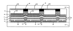
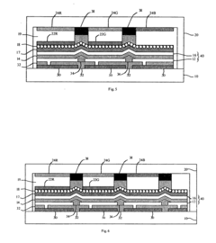
OLED device having improved light output
PatentInactiveUS20070103056A1
Innovation
- A full-color OLED device structure featuring patterned electrodes, unpatterned organic material layers emitting broadband light, color-change materials, and a blue color filter to directly filter emitted light, combined with a scattering layer and low-index element to extract trapped light and improve sharpness.
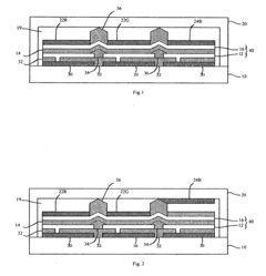
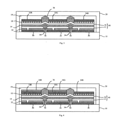
Micro light-emitting diode display with 3D orifice plating and light filtering
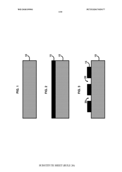
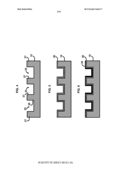
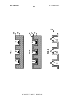
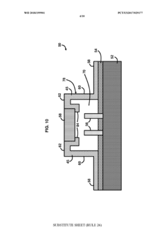
PatentWO2018199901A1
Innovation
- A 3D orifice plating with a metal housing and integrated RGB filters is used, where the electroplating process creates a non-transparent metal housing with specific orifices and notches for filters, allowing direct light transmission through translucent filters without refraction, enabling improved light concentration and filtering.
Intellectual Property Landscape in Display Technologies
The intellectual property landscape in display technologies, particularly concerning OLED and MicroLED, has evolved into a complex ecosystem of patents, licensing agreements, and strategic positioning. Major technology companies have amassed substantial patent portfolios to protect their innovations and secure competitive advantages in this rapidly evolving market.
Samsung Display and LG Display dominate the OLED patent landscape, collectively holding over 60% of fundamental OLED patents worldwide. These patents cover critical aspects including pixel structures, thin-film transistor designs, and manufacturing processes. Apple has strategically acquired display-related patents while simultaneously entering into licensing agreements with these Korean giants to secure supply chains for their devices.
In the emerging MicroLED space, the patent landscape is more fragmented but increasingly competitive. Companies like Apple, Samsung, and Sony have been aggressively filing patents related to mass transfer techniques - the critical manufacturing challenge for MicroLED commercialization. Notable acquisitions include Apple's purchase of LuxVue Technology in 2014, which provided them with foundational MicroLED patents.
Standards-essential patents (SEPs) play a crucial role in display technology development, with organizations like VESA (Video Electronics Standards Association) and JEDEC establishing technical specifications that manufacturers must adhere to. Companies holding SEPs can significantly influence industry direction while generating substantial licensing revenue.
Cross-licensing agreements have become increasingly common as companies seek to navigate the complex patent landscape without engaging in costly litigation. These agreements often involve significant financial transactions and technology sharing arrangements between major players.
Patent litigation in display technologies has intensified as the market grows. Notable cases include Universal Display Corporation's OLED phosphorescent materials patents, which have been licensed to virtually all major OLED manufacturers, and various disputes over quantum dot enhancement film technologies used in premium displays.
Regional differences in patent protection strategies are evident, with Chinese display manufacturers rapidly increasing their patent filings while focusing on manufacturing process innovations. Meanwhile, Japanese and Korean companies maintain strong positions in materials science patents, and U.S. companies lead in system-level integration and user interface patents.
The intellectual property landscape will continue to evolve as new display technologies emerge, with particular attention to innovations addressing power efficiency, brightness, and manufacturing scalability - areas where both OLED and MicroLED technologies face ongoing challenges.
Environmental Impact and Sustainability Considerations
The environmental impact of display technologies has become increasingly important as sustainability considerations gain prominence in both consumer choices and regulatory frameworks. OLED and MicroLED technologies present distinct environmental profiles throughout their lifecycle, from raw material extraction to end-of-life disposal.
Manufacturing processes for OLED displays typically involve fewer toxic materials compared to traditional LCD technology, but still utilize rare earth elements and organic compounds that present extraction challenges. MicroLED manufacturing currently requires more energy-intensive processes due to the precision needed for placing millions of microscopic LEDs, though this may improve with technological advancement and economies of scale.
Energy efficiency represents a critical environmental consideration where both technologies offer advantages. OLEDs consume minimal power when displaying dark content due to their ability to completely turn off individual pixels. MicroLEDs potentially surpass OLEDs in efficiency by delivering higher brightness with lower power consumption, particularly important for mobile devices and wearables where battery life is paramount.
Lifespan differences significantly impact sustainability metrics. OLED displays typically suffer from organic material degradation, leading to shorter lifespans and more frequent replacement cycles. MicroLEDs promise substantially longer operational lives, potentially reducing electronic waste generation over time. This longevity advantage could offset MicroLED's initially higher environmental manufacturing footprint through extended product lifecycles.
Recycling capabilities vary between technologies. OLED panels present challenges for material recovery due to their complex organic layers and thin-film construction. MicroLED displays, while also complex, contain more recoverable inorganic materials that may prove easier to recycle with appropriate infrastructure development.
Emerging standards are beginning to address these environmental considerations. The EPEAT registry and Energy Star certifications are expanding criteria to evaluate display technologies based on energy efficiency, material selection, and end-of-life management. The European Union's Ecodesign Directive is also evolving to incorporate specific requirements for next-generation display technologies.
Industry initiatives are developing in response to these concerns. Major manufacturers are investing in closed-loop recycling programs and exploring bio-based materials for OLED production. Research into less energy-intensive MicroLED manufacturing processes is accelerating, with promising developments in transfer techniques that could significantly reduce environmental impact while maintaining performance advantages.
Unlock deeper insights with Patsnap Eureka Quick Research — get a full tech report to explore trends and direct your research. Try now!
Generate Your Research Report Instantly with AI Agent
Supercharge your innovation with Patsnap Eureka AI Agent Platform!