Analysis of OLED vs MicroLED Integration in Mobile Tech
OCT 24, 20259 MIN READ
Generate Your Research Report Instantly with AI Agent
Patsnap Eureka helps you evaluate technical feasibility & market potential.
OLED and MicroLED Evolution and Objectives
Display technology in mobile devices has undergone significant evolution since the introduction of the first smartphones. OLED (Organic Light Emitting Diode) technology emerged as a revolutionary advancement over traditional LCD displays, offering superior contrast ratios, wider viewing angles, and the ability to produce true blacks by completely turning off pixels. The first commercial OLED displays in mobile devices appeared in the late 2000s, with Samsung and LG leading the charge in development and mass production.
OLED technology has since evolved through several generations, from passive-matrix OLED (PMOLED) to active-matrix OLED (AMOLED), and further to flexible OLED panels that enable curved and foldable displays. The introduction of LTPO (Low-Temperature Polycrystalline Oxide) OLED technology marked another significant milestone, allowing for variable refresh rates that substantially improve power efficiency in mobile devices.
MicroLED represents the next frontier in display technology, promising to overcome some inherent limitations of OLED. Developed initially for large-format displays, MicroLED utilizes microscopic LED arrays that are self-emissive like OLED but composed of inorganic materials. The technology was first demonstrated in laboratory settings in the early 2010s, with companies like Sony and Samsung showcasing prototype displays at major technology exhibitions.
The technical evolution trajectory suggests a gradual transition from OLED to MicroLED in premium mobile devices over the next decade. This shift is driven by MicroLED's theoretical advantages in brightness (up to 30 times brighter than OLED), longevity (no organic material degradation), and energy efficiency (potentially 50% more efficient than current OLED implementations).
The primary objectives for both technologies in mobile integration center around several key parameters. For OLED, the focus remains on addressing burn-in issues, improving peak brightness while maintaining energy efficiency, and reducing production costs to maintain competitive pricing in mid-range devices. The industry is also pursuing advancements in flexible OLED technology to enable more innovative form factors.
For MicroLED, the primary objectives involve overcoming significant manufacturing challenges, particularly in achieving mass production with consistent quality at the microscopic scale required for mobile devices. Reducing the pixel pitch to match or exceed current OLED resolutions while maintaining perfect yield rates represents a formidable technical challenge. Additionally, the industry aims to develop transfer processes that can efficiently place millions of tiny LEDs precisely onto substrates at economically viable costs.
Both technologies are evolving toward enabling higher refresh rates, improved color accuracy with wider gamut coverage, and reduced power consumption – all critical factors for next-generation mobile experiences that will incorporate augmented reality and other computationally intensive applications.
Mobile Display Market Demand Analysis
The mobile display market has witnessed significant growth over the past decade, driven primarily by smartphone proliferation and increasing consumer demand for superior visual experiences. Current market analysis indicates that the global smartphone display market is valued at approximately 50 billion USD, with projections suggesting growth to reach 70 billion USD by 2027, representing a compound annual growth rate of 7.2%.
Consumer preferences have evolved dramatically, with high-resolution, vibrant displays becoming a decisive factor in purchasing decisions. Market surveys reveal that over 65% of consumers consider display quality among the top three features influencing their smartphone selection, surpassing even battery life and camera capabilities in certain demographic segments.
OLED technology currently dominates the premium smartphone segment, with Samsung Display and LG Display controlling nearly 90% of the OLED supply chain. The technology's advantages in producing vibrant colors, perfect blacks, and enabling flexible form factors have cemented its position in flagship devices. However, OLED displays face persistent challenges including burn-in issues, limited lifespan, and relatively high production costs.
MicroLED represents the emerging disruptive technology in this space, with market forecasts predicting its value to grow from 600 million USD in 2023 to potentially 10 billion USD by 2030. The technology promises superior brightness (up to 30% brighter than OLED), longer lifespan (100,000+ hours versus 30,000 for OLED), and improved energy efficiency. Despite these advantages, current adoption remains limited due to prohibitive manufacturing costs and technical challenges in miniaturization.
Regional analysis shows varying adoption patterns, with Asian markets demonstrating higher sensitivity to display innovations. North American consumers exhibit stronger willingness to pay premium prices for advanced display technologies, while European markets show more balanced consideration between display quality and device longevity.
Industry forecasts indicate a potential shift in market dynamics as MicroLED manufacturing processes mature. Production costs are expected to decrease by approximately 40% over the next five years as economies of scale improve and manufacturing techniques advance. This cost reduction trajectory could position MicroLED as a viable alternative to OLED in premium devices by 2026-2027.
The sustainability aspect is increasingly influencing market demand, with MicroLED's longer lifespan and lower energy consumption aligning with growing consumer environmental consciousness. Market research indicates that 47% of consumers under 35 consider environmental impact in their purchasing decisions, potentially accelerating MicroLED adoption once price points become more accessible.
Current Technical Limitations and Challenges
The integration of display technologies in mobile devices faces significant technical limitations that differentiate OLED and MicroLED implementations. OLED technology, while mature in the mobile market, continues to struggle with several persistent challenges. Burn-in remains a critical issue where static images can cause permanent damage to pixels over time, particularly affecting user interfaces with static elements. Additionally, OLED displays typically experience brightness degradation, with blue subpixels deteriorating faster than others, leading to color shifts throughout the device's lifespan.
Power efficiency presents another challenge for OLED displays, especially when displaying bright content. While OLEDs excel in power efficiency when displaying dark content due to their ability to turn off individual pixels, they consume significantly more power when displaying bright or white screens, which impacts battery life in mobile devices.
MicroLED technology, though promising, faces even more substantial barriers to widespread mobile integration. Manufacturing yield rates remain prohibitively low, with the precise placement of millions of microscopic LEDs proving extremely challenging. Current production processes struggle to achieve the necessary precision at scale, resulting in high defect rates and consequently elevated costs that make mass production economically unfeasible for consumer mobile devices.
Size reduction represents another significant hurdle for MicroLED. While the technology has made inroads in larger displays, miniaturizing LEDs to the pixel densities required for mobile devices (often exceeding 400 PPI) while maintaining brightness uniformity and color accuracy presents formidable engineering challenges.
Heat management constitutes a shared challenge for both technologies but manifests differently. OLED displays generate heat during operation that can accelerate pixel degradation, while MicroLED systems require sophisticated thermal management solutions to dissipate heat from densely packed LED arrays, particularly challenging within the confined spaces of mobile devices.
From a supply chain perspective, OLED manufacturing has consolidated around a few key players, creating potential bottlenecks and pricing pressures. MicroLED faces even greater supply chain constraints with limited manufacturing capacity and specialized equipment requirements, further complicating its path to market viability.
Color accuracy and reproduction present ongoing challenges for both technologies. OLED displays can suffer from color shifts at different viewing angles and brightness levels, while MicroLED technology still requires refinement in color calibration and consistency across the millions of individual emitters that comprise a display.
Current Integration Solutions for Mobile Devices
01 OLED display structure and materials
OLED (Organic Light Emitting Diode) displays utilize organic compounds that emit light when an electric current is applied. These displays feature multiple layers including cathode, organic layers, and anode. The organic materials can be designed to emit different colors, eliminating the need for backlighting and color filters used in traditional LCD displays. This structure allows for thinner, more flexible displays with better contrast ratios and wider viewing angles.- OLED display structure and materials: Organic Light Emitting Diode (OLED) displays utilize organic compounds that emit light when electricity is applied. These displays feature multiple layers including cathode, organic layers, and anode. The organic materials can be engineered for different colors and brightness levels. OLED technology offers advantages such as flexibility, thinness, and high contrast ratios compared to traditional display technologies. Various improvements in OLED materials and structures have been developed to enhance efficiency and lifespan.
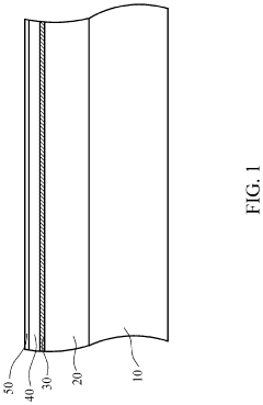
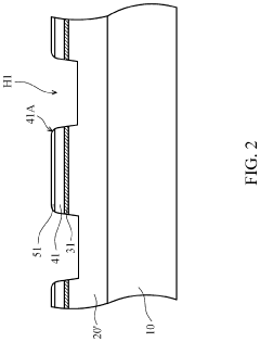
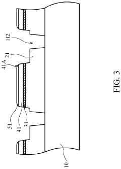
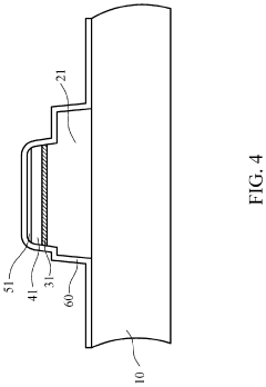
- MicroLED fabrication and integration: MicroLED displays consist of arrays of microscopic LED elements that serve as individual pixels. The fabrication process involves creating tiny LED structures, typically less than 100 micrometers, and transferring them to a display substrate. Various methods have been developed for mass transfer of these micro-scale LEDs to achieve efficient manufacturing. The integration challenges include precise alignment, electrical connections, and maintaining high yield rates during the transfer process.
- Display driving and control systems: Advanced driving and control systems are essential for both OLED and MicroLED displays. These systems include thin-film transistor (TFT) backplanes, driving circuits, and control algorithms that manage pixel addressing, brightness control, and power management. Innovations in this area focus on reducing power consumption, improving refresh rates, and enabling high dynamic range (HDR) capabilities. The driving systems also address challenges such as non-uniformity correction and compensation for aging effects in display elements.
- Flexible and foldable display technologies: Both OLED and MicroLED technologies can be implemented in flexible and foldable display configurations. These displays use specialized substrates and encapsulation methods to enable bending without damaging the light-emitting elements. The development includes flexible backplanes, bendable encapsulation layers, and stress-resistant electrode materials. These technologies enable new form factors for devices such as smartphones, wearables, and other consumer electronics with curved, rollable, or foldable screens.
- Thermal management and efficiency improvements: Thermal management is crucial for both OLED and MicroLED displays to ensure optimal performance and longevity. Various approaches have been developed to dissipate heat effectively, including specialized heat sinks, thermal interface materials, and optimized circuit designs. Efficiency improvements focus on reducing power consumption while maintaining or enhancing brightness levels. These innovations include better light extraction methods, improved electron-hole recombination efficiency, and advanced power management algorithms.
02 MicroLED fabrication and integration
MicroLED technology involves the integration of microscopic LED arrays to create displays with high brightness and energy efficiency. The fabrication process includes the transfer of tiny LED chips onto a substrate and establishing electrical connections. Various methods are employed to improve yield rates and reduce manufacturing costs, including mass transfer techniques and pick-and-place processes. These displays offer advantages such as higher brightness, longer lifespan, and better energy efficiency compared to other display technologies.Expand Specific Solutions03 Display driver circuits and control systems
Advanced driver circuits and control systems are essential for both OLED and MicroLED displays to manage pixel addressing, brightness control, and color reproduction. These systems include thin-film transistor (TFT) backplanes, integrated circuits for signal processing, and sophisticated algorithms for image quality enhancement. The control systems also manage power consumption and implement features such as adaptive brightness and refresh rates to optimize display performance under various conditions.Expand Specific Solutions04 Flexible and foldable display technologies
Both OLED and MicroLED technologies can be implemented in flexible and foldable display configurations. These displays use specialized substrates and encapsulation methods to maintain functionality while being bent or folded. The development includes innovative approaches to handle mechanical stress at fold points, prevent pixel damage during repeated folding, and maintain consistent image quality across the entire display surface. These advancements enable new form factors for mobile devices, wearables, and other consumer electronics.Expand Specific Solutions05 Energy efficiency and heat management
Energy efficiency and thermal management are critical aspects of OLED and MicroLED display technologies. Various approaches are implemented to reduce power consumption while maintaining display brightness and quality. Heat dissipation techniques are employed to prevent performance degradation and extend the lifespan of the displays. These include optimized pixel designs, efficient driver circuits, and advanced materials that can operate at lower power levels while delivering high brightness and color accuracy.Expand Specific Solutions
Key Industry Players and Ecosystem
The OLED vs MicroLED integration in mobile technology market is currently in a transitional phase, with OLED being mature and widely adopted while MicroLED remains in early commercialization. The global market is projected to reach $200 billion by 2025, driven by demand for higher display performance in smartphones and wearables. In terms of technical maturity, companies like Samsung, Apple, and BOE lead OLED production with established manufacturing capabilities, while MicroLED development is being pioneered by Samsung, Apple, and X Display Co. through significant R&D investments. Intel, TCL, and Japan Display are also making strategic advancements in both technologies, focusing on efficiency improvements and production scaling to overcome MicroLED's current cost barriers.
BOE Technology Group Co., Ltd.
Technical Solution: BOE has developed flexible OLED technology with integrated touch functionality using their self-developed LTPO (Low-Temperature Polycrystalline Oxide) backplane technology, enabling variable refresh rates from 1-120Hz in mobile displays. Their OLED panels achieve brightness levels exceeding 1,500 nits while maintaining power efficiency through pixel-level current control algorithms. For MicroLED, BOE has established a comprehensive technology platform covering chip manufacturing, mass transfer processes, and driving circuit integration. Their MicroLED approach utilizes a proprietary "micro-repair" technology that addresses yield issues by allowing for individual defective pixel replacement during manufacturing. BOE has demonstrated MicroLED displays with pixel pitches below 40 micrometers suitable for mobile applications, achieving brightness exceeding 3,000 nits while maintaining color accuracy across viewing angles. Their mass transfer process employs a selective laser-assisted transfer method that can position thousands of MicroLED chips simultaneously with micron-level precision, addressing one of the key manufacturing challenges for mobile-scale implementation.
Strengths: BOE possesses extensive manufacturing capacity and a complete supply chain for both OLED and MicroLED production, allowing for economies of scale. Their government-backed funding enables sustained long-term R&D investment in next-generation display technologies. Weaknesses: BOE's MicroLED technology still faces cost challenges for mass production at mobile device scales, with current implementations primarily targeting premium market segments. Their intellectual property position in some advanced display technologies remains behind some competitors.
Japan Display, Inc.
Technical Solution: Japan Display (JDI) has developed advanced OLED technologies including their FULL ACTIVE™ flexible OLED displays featuring ultra-narrow bezels and in-cell touch technology specifically optimized for mobile applications. Their proprietary pixel structure achieves high color accuracy (covering over 100% of DCI-P3) while implementing current compensation circuits that extend panel lifetime by preventing pixel degradation. JDI's OLED panels incorporate transparent circuit technology that increases light transmission efficiency, resulting in lower power consumption for equivalent brightness levels compared to conventional designs. For MicroLED development, JDI leverages their expertise in LCD manufacturing to create hybrid solutions that combine traditional LCD backplanes with MicroLED light sources. Their approach utilizes a unique "chip-last" transfer process where the display substrate is prepared with all necessary circuitry before precision placement of MicroLED elements, potentially improving manufacturing yields. JDI has demonstrated MicroLED prototypes with pixel densities exceeding 300 PPI while maintaining brightness uniformity within ±5% across the display surface, addressing a key challenge for mobile implementations where viewing distance makes uniformity issues more noticeable.
Strengths: JDI possesses extensive experience in high-volume mobile display manufacturing and quality control processes that transfer well to new technologies. Their established relationships with major mobile device manufacturers provide clear commercialization pathways. Weaknesses: JDI's financial constraints have limited R&D investment compared to some competitors, potentially slowing their technology advancement. Their MicroLED manufacturing approach still requires significant refinement to reach cost parity with current display technologies.
Critical Patents and Innovations in Display Technology
Micro light-emitting diode structure and micro light-emitting diode display device using the same
PatentInactiveUS20220173273A1
Innovation
- A flip-chip micro light-emitting diode structure is designed where the mesa region is smaller than the first-type semiconductor layer, exposing a portion of its top surface for electrode connection, eliminating the need for multiple aligned holes and simplifying the manufacturing process.
Micro light-emitting diode display device and micro light-emitting diode driving circuit
PatentActiveUS10680035B1
Innovation
- A micro light-emitting diode display device with a driving transistor featuring a gate insulator thickness of less than or equal to 500 angstroms and a micro light-emitting diode with a current injection channel and an active layer portion in contact with the channel, reducing the light-emitting area and avoiding surface recombination, thereby lowering the voltage required to activate the diode.
Manufacturing Process Comparison
The manufacturing processes for OLED and MicroLED displays represent significantly different technological approaches, with distinct implications for mobile device integration. OLED manufacturing has matured considerably over the past decade, utilizing established vapor deposition techniques where organic materials are deposited onto glass substrates in vacuum chambers. This process has been refined to achieve high yields at scale, particularly for small to medium-sized displays suitable for smartphones and wearables.
The OLED manufacturing workflow typically involves TFT backplane fabrication, followed by organic material deposition through either vacuum thermal evaporation (VTE) for small molecule OLEDs or solution processing for polymer-based variants. The process concludes with encapsulation to protect the sensitive organic materials from oxygen and moisture degradation. Major manufacturers have achieved impressive production efficiencies, with Samsung Display and LG Display operating massive Gen 6+ fabs capable of producing millions of panels monthly.
In contrast, MicroLED manufacturing remains in earlier developmental stages, facing considerable challenges in mass production. The process involves fabricating microscopic LED arrays (typically 3-10 μm in size), transferring these tiny elements from growth substrates to display backplanes, and establishing reliable electrical connections. The mass transfer process represents the most significant manufacturing hurdle, with various approaches being explored including stamp transfer, laser-assisted transfer, and fluid-assisted assembly.
MicroLED production currently suffers from lower yields and higher defect rates compared to OLED. The precision required to place millions of microscopic LEDs accurately presents unprecedented manufacturing challenges. For a typical smartphone display with 4K resolution, over 24 million individual MicroLEDs must be transferred with near-perfect accuracy, where even 99.9% yield would result in thousands of defects requiring repair.
Cost structures differ substantially between the technologies. OLED manufacturing benefits from economies of scale and established supply chains, with production costs declining approximately 15-20% annually. MicroLED production remains prohibitively expensive for mass-market mobile devices, with estimates suggesting costs 5-8 times higher than equivalent OLED displays in current manufacturing scenarios.
Equipment requirements also diverge significantly. OLED production relies on modified semiconductor manufacturing equipment, while MicroLED requires development of specialized mass transfer equipment and inspection systems capable of identifying and repairing defective pixels at unprecedented scales. Companies like Apple, Samsung, and PlayNitride are investing heavily in proprietary manufacturing solutions to overcome these challenges.
Energy Efficiency and Environmental Impact
Energy efficiency represents a critical factor in the evaluation of display technologies for mobile devices, where battery life directly impacts user experience. OLED technology has traditionally held an advantage in this domain due to its self-emissive nature, which allows individual pixels to be completely turned off when displaying black content. This pixel-level power management enables OLED displays to achieve significant energy savings, particularly when displaying dark-themed content or using features like Always-On Display with minimal active pixels.
MicroLED technology promises to further advance energy efficiency paradigms in mobile displays. Initial research indicates that MicroLED displays can achieve up to 30% greater energy efficiency compared to OLED counterparts when operating at similar brightness levels. This efficiency stems from MicroLED's superior light emission mechanism, which converts more electrical energy directly into visible light with reduced heat generation.
The environmental impact assessment of these technologies reveals notable differences throughout their lifecycle. OLED manufacturing processes currently involve organic solvents and potentially hazardous materials that require careful handling and disposal. The production facilities demand extensive clean room environments with high energy consumption. Additionally, the limited lifespan of organic materials in OLEDs contributes to replacement frequency and subsequent electronic waste.
MicroLED manufacturing presents its own environmental challenges, particularly in the precise transfer and placement of millions of microscopic LED elements. However, the technology offers environmental advantages through extended operational lifespans—potentially exceeding 100,000 hours compared to OLED's typical 30,000-50,000 hours—which could significantly reduce electronic waste over time. The inorganic materials used in MicroLEDs are also generally more recyclable than their organic counterparts.
Carbon footprint analysis across the full lifecycle reveals that while initial manufacturing emissions may be higher for MicroLED due to complex production processes, the extended lifespan and superior energy efficiency during operation may result in a lower overall environmental impact. This becomes particularly relevant as mobile devices increasingly serve as primary computing platforms with longer daily usage hours.
For mobile technology integration, these efficiency and environmental considerations translate directly to practical benefits. Improved energy efficiency extends device battery life, potentially reducing charging frequency and associated energy consumption. The durability advantage of MicroLED could extend device replacement cycles, addressing growing concerns about electronic waste in the technology sector.
Unlock deeper insights with Patsnap Eureka Quick Research — get a full tech report to explore trends and direct your research. Try now!
Generate Your Research Report Instantly with AI Agent
Supercharge your innovation with Patsnap Eureka AI Agent Platform!