

What Are OLED vs MicroLED's Key Technical Challenges
OCT 24, 20259 MIN READ
Generate Your Research Report Instantly with AI Agent
Patsnap Eureka helps you evaluate technical feasibility & market potential.
OLED and MicroLED Evolution and Development Goals
The display industry has witnessed significant technological evolution over the past decades, transitioning from CRT to LCD, and now advancing toward OLED and MicroLED technologies. OLED (Organic Light Emitting Diode) technology emerged commercially in the early 2000s, pioneered by companies like Kodak and Samsung, and has since become mainstream in premium smartphones, televisions, and wearable devices. MicroLED, a more recent innovation, represents the next frontier in display technology, promising superior performance across multiple parameters.
OLED technology has evolved through several generations, from passive-matrix to active-matrix designs, with significant improvements in efficiency, lifespan, and color reproduction. The development trajectory has focused on overcoming inherent limitations such as blue pixel degradation, burn-in issues, and manufacturing scalability. Recent advancements include the introduction of TADF (Thermally Activated Delayed Fluorescence) materials and solution-processed OLEDs, aiming to reduce production costs while maintaining performance.
MicroLED technology, conceptualized in the early 2000s but only recently approaching commercial viability, represents a fundamental shift in display architecture. Unlike OLEDs, MicroLEDs utilize inorganic gallium nitride-based LEDs at microscopic scales (typically <50 μm), offering theoretical advantages in brightness, efficiency, and longevity. The evolution of MicroLED has been characterized by progressive miniaturization of LED chips and development of mass transfer techniques to enable practical manufacturing.
The technical goals for OLED development include extending operational lifespan beyond 100,000 hours, achieving power efficiency exceeding 200 lm/W, developing blue emitters with comparable stability to red and green counterparts, and establishing cost-effective large-scale production methods for displays exceeding 65 inches. Additionally, enhancing flexibility and transparency while maintaining performance metrics remains a priority for expanding application scenarios.
For MicroLED, development goals center on reducing pixel pitch below 5 μm, improving mass transfer yields to over 99.9999%, developing efficient repair processes for defective pixels, and dramatically reducing production costs to compete with premium OLED displays. Concurrent objectives include perfecting full-color solutions without efficiency loss and scaling manufacturing capabilities to support diverse display sizes from microdisplays to large-format screens.
The convergence point for both technologies lies in achieving perfect black levels, wide color gamut (>95% Rec.2020), high brightness (>2,000 nits), microsecond response times, and energy efficiency that enables extended battery life in portable devices or reduced power consumption in fixed installations. The ultimate technical goal is to develop displays that perfectly replicate human visual perception capabilities while minimizing resource utilization.
Market Demand Analysis for Advanced Display Technologies
The display technology market is witnessing a significant shift towards advanced solutions that offer superior visual experiences across multiple applications. Current market analysis indicates robust demand growth for both OLED and MicroLED technologies, driven primarily by consumer electronics, automotive displays, and professional visualization sectors.
Consumer electronics remains the dominant market segment, with smartphones accounting for approximately 60% of OLED panel shipments. The premium smartphone market has almost universally adopted OLED technology, with manufacturers competing to deliver higher screen-to-body ratios and innovative form factors including foldable and rollable displays. This trend is expected to continue as consumers increasingly prioritize display quality in purchase decisions.
Television displays represent another critical growth segment, with OLED TVs establishing a strong presence in the high-end market. However, MicroLED is positioned to challenge this dominance, particularly in the ultra-premium segment where price sensitivity is lower. Market research indicates that consumers are willing to pay premium prices for displays offering perfect blacks, wider color gamut, and higher brightness levels – attributes that both technologies can deliver through different approaches.
The automotive sector presents a rapidly expanding opportunity for advanced display technologies. The transition toward smart cockpits and autonomous vehicles is driving demand for larger, curved, and irregularly shaped displays that can be seamlessly integrated into vehicle interiors. OLED's flexibility advantage currently dominates this space, but MicroLED's superior brightness and longevity make it increasingly attractive for automotive applications where displays must function reliably in high-ambient light conditions.
Commercial and professional markets show growing demand for large-format displays with exceptional visual performance. Digital signage, control rooms, and simulation environments require displays with high brightness, wide viewing angles, and excellent color accuracy – creating opportunities for both technologies but particularly favoring MicroLED's scalability advantages.
Healthcare and aerospace sectors represent emerging niche markets with stringent requirements for display reliability and performance under extreme conditions. These specialized applications often justify the higher costs associated with cutting-edge display technologies, creating valuable development opportunities despite smaller volume potential.
Regional analysis reveals that East Asia continues to lead in both production capacity and consumption of advanced displays, with North America and Europe following as premium markets. Developing economies are showing accelerated adoption rates as manufacturing efficiencies gradually reduce costs.
The overall market trajectory suggests a compound annual growth rate exceeding 15% for advanced display technologies through 2028, with MicroLED expected to show the most dramatic growth curve as manufacturing challenges are progressively overcome. This growth is supported by broader technology trends including augmented reality, virtual reality, and the increasing digitization of physical environments across multiple industries.
Technical Barriers and Global Development Status
OLED technology currently dominates the high-end display market due to its mature manufacturing processes and established supply chains. However, it faces significant technical barriers including limited lifespan, particularly for blue OLED materials which degrade faster than red and green counterparts. This differential aging leads to color shifts over time, compromising display quality. Additionally, OLED displays suffer from burn-in issues when static images are displayed for extended periods, and their organic materials are susceptible to moisture and oxygen degradation, necessitating complex encapsulation solutions.
MicroLED technology, while promising superior performance, confronts even more formidable challenges. Mass transfer remains the most significant barrier—efficiently moving millions of tiny LED chips from growth substrates to display backplanes with precise positioning and high yield rates. Current approaches including stamp transfer, laser transfer, and fluid assembly each have limitations in scalability, accuracy, or throughput. The industry has yet to establish a definitive solution for high-volume manufacturing.
Size reduction presents another critical challenge for MicroLED. As pixel sizes decrease below 10 microns, efficiency drops dramatically due to increased surface defects relative to volume. This "sidewall effect" significantly impacts quantum efficiency and brightness. Furthermore, achieving consistent color performance across millions of individual LEDs requires unprecedented uniformity in manufacturing.
Globally, OLED development is concentrated in East Asia, with South Korean companies like Samsung and LG leading in mobile and large-format displays respectively. Japanese firms focus on materials development, while Chinese manufacturers rapidly expand production capacity. The United States maintains strength in intellectual property and specialized applications.
MicroLED development shows a different geographic distribution. Taiwan and Japan lead in epitaxial growth technology, while European research institutions have made significant contributions to transfer technology. American companies, particularly Apple and startups like Luxvue, have accumulated substantial intellectual property portfolios through strategic acquisitions.
The technology readiness level (TRL) differs significantly between these technologies. OLED has reached TRL 9 with full commercial deployment, while MicroLED remains between TRL 6-7, with demonstration systems and limited production but lacking mature mass-production capabilities. Industry consensus suggests MicroLED requires 3-5 more years of development before achieving cost-effective mass production for consumer applications.
Current Technical Solutions for OLED and MicroLED
01 Manufacturing challenges in MicroLED displays
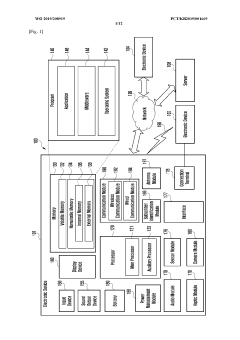
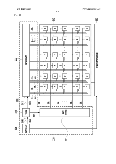
MicroLED displays face significant manufacturing challenges including mass transfer of tiny LED chips, precise placement accuracy, and yield management. The miniaturization of LED chips to microscale dimensions creates difficulties in handling and positioning these components with the required precision. Additionally, the manufacturing process must address issues related to defect detection, repair strategies, and maintaining consistent performance across large display areas.- Manufacturing challenges in MicroLED displays: MicroLED displays face significant manufacturing challenges including mass transfer of tiny LED chips, precise placement accuracy, and yield management. The miniaturization of LED chips to microscale dimensions creates difficulties in handling and positioning these components with the required precision. Additionally, achieving consistent performance across millions of individual LEDs on a display panel remains a technical hurdle, affecting production yields and costs.
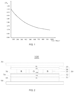
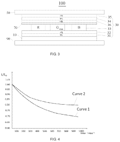
- OLED material degradation and lifetime issues: OLED displays suffer from material degradation issues that affect their longevity and performance. Organic materials in OLEDs are susceptible to degradation from oxygen, moisture, and prolonged use, leading to reduced brightness and color shifts over time. Different color-emitting materials degrade at different rates, causing display uniformity problems. Addressing these degradation mechanisms requires advanced encapsulation techniques and material innovations to extend the operational lifetime of OLED displays.
- Power efficiency and heat management: Both OLED and MicroLED technologies face challenges related to power efficiency and heat management. While these technologies are generally more efficient than traditional displays, achieving optimal power consumption while maintaining brightness remains challenging. Heat generation during operation can accelerate material degradation and affect display performance. Advanced thermal management solutions and circuit designs are needed to dissipate heat effectively and improve overall energy efficiency.
- Color accuracy and uniformity challenges: Maintaining consistent color accuracy and uniformity across the entire display area presents significant technical challenges for both OLED and MicroLED technologies. Variations in manufacturing processes can lead to pixel-to-pixel inconsistencies in brightness and color reproduction. For MicroLEDs, the challenge involves ensuring uniform performance across millions of individual LED elements, while OLEDs struggle with differential aging of organic materials that can cause color shifts over time.
- Integration and scaling challenges: Scaling production and integrating these advanced display technologies into various form factors present significant technical hurdles. For MicroLEDs, the challenge lies in scaling down the pixel size while maintaining efficiency and brightness. For OLEDs, creating flexible and foldable displays requires specialized substrates and encapsulation methods. Both technologies face integration challenges with touch sensors, cameras, and other components that need to be embedded within or behind the display while maintaining optimal performance.
02 OLED material degradation and lifetime issues
OLED displays face technical challenges related to material degradation over time, particularly with blue emitters which typically have shorter lifespans than red and green counterparts. This degradation leads to color shift, reduced brightness, and display non-uniformity with extended use. The organic materials are also susceptible to moisture and oxygen, requiring advanced encapsulation technologies to protect the sensitive components and extend the operational lifetime of the display.Expand Specific Solutions03 Power efficiency and heat management
Both OLED and MicroLED technologies face challenges related to power efficiency and heat management. While MicroLEDs offer theoretical advantages in power consumption, achieving this efficiency at scale remains challenging. Heat dissipation is critical for maintaining display performance and longevity, particularly in high-brightness applications. Advanced thermal management solutions and more efficient driving methods are being developed to address these issues and optimize power consumption.Expand Specific Solutions04 Color accuracy and quantum dot integration
Achieving consistent color accuracy across the display area presents challenges for both technologies. For MicroLEDs, the integration of quantum dots is being explored to enhance color performance and efficiency. This approach involves developing compatible materials and processes to combine quantum dot color conversion layers with LED chips. The challenge lies in maintaining color uniformity, wide color gamut, and high efficiency while ensuring manufacturing feasibility at scale.Expand Specific Solutions05 Flexible and transparent display implementation
Implementing flexible and transparent displays using OLED and MicroLED technologies presents unique technical challenges. These include developing suitable substrate materials, ensuring mechanical durability during bending, and maintaining electrical connectivity in flexible conditions. For transparent displays, balancing transparency with display performance requires innovative approaches to electrode design and light management. These advanced form factors demand specialized manufacturing processes and materials to achieve the desired performance characteristics.Expand Specific Solutions
Leading Manufacturers and Competitive Landscape
The OLED vs MicroLED display technology landscape is currently in a transitional phase, with OLED being mature and commercially established while MicroLED remains in early commercialization. The global market for these advanced display technologies is projected to exceed $200 billion by 2025, driven by demand for higher performance displays. Technologically, companies like Samsung and BOE lead OLED production with established manufacturing processes, while MicroLED faces significant challenges in mass transfer techniques, yield rates, and cost reduction. Companies including Apple, Samsung, and TCL are investing heavily in MicroLED R&D, with specialized firms like eLux and Lumileds developing innovative assembly solutions. The competition is intensifying as display manufacturers seek to overcome MicroLED's technical barriers while leveraging OLED's existing advantages.
BOE Technology Group Co., Ltd.
Technical Solution: BOE has developed advanced solutions for both OLED and MicroLED technologies. For OLED, BOE employs flexible AMOLED technology with oxide TFT backplanes that enable ultra-thin, flexible displays with reduced power consumption. Their OLED panels feature pixel densities exceeding 400 PPI with response times under 0.1ms. BOE has pioneered printed OLED manufacturing techniques to reduce production costs by approximately 30% compared to traditional vacuum deposition methods[2]. For MicroLED, BOE has developed a proprietary "active matrix" architecture using GaN-based LED chips with sizes ranging from 30-50 micrometers. Their MicroLED technology incorporates a unique mass transfer process utilizing electrostatic forces for precise placement, achieving transfer yields above 95% for RGB chips. BOE has also developed specialized thin-film encapsulation techniques for MicroLED to enhance durability and lifespan, with reported operational lifetimes exceeding 100,000 hours while maintaining over 95% of original brightness. Their MicroLED displays achieve brightness levels of 1,500-2,000 nits with power efficiency improvements of approximately 25-30% compared to their OLED counterparts.
Strengths: BOE possesses extensive manufacturing capacity with multiple Gen 6 and Gen 8.5 production lines, enabling significant production scale. Their strong R&D capabilities have yielded over 10,000 display-related patents. Weaknesses: BOE's MicroLED mass transfer technology still faces yield challenges at commercial production scales, with defect rates higher than industry leaders. Their color consistency and uniformity in large MicroLED panels remain inferior to Samsung's offerings, particularly in achieving balanced white point accuracy.
Wuhan China Star Optoelectronics Technology Co., Ltd.
Technical Solution: Wuhan China Star Optoelectronics (CSOT) has developed comprehensive solutions addressing both OLED and MicroLED technical challenges. For OLED, CSOT employs advanced LTPS (Low-Temperature Polysilicon) backplane technology combined with inkjet-printed RGB emissive materials, achieving pixel densities of 300-400 PPI with reduced production costs. Their OLED panels feature specialized color filters that enhance color gamut coverage to approximately 110% DCI-P3 while maintaining brightness levels of 600-800 nits[3]. CSOT has also developed proprietary thin-film encapsulation techniques that extend OLED panel lifespans by approximately 30% compared to industry standards. For MicroLED, CSOT utilizes a hybrid integration approach combining traditional pick-and-place methods with fluidic self-assembly techniques for LED chips sized between 40-70 micrometers. Their MicroLED technology incorporates a unique redundancy architecture that improves yield rates by approximately 15-20% by compensating for defective pixels during the manufacturing process. CSOT has developed specialized phosphor conversion techniques for their MicroLED displays that simplify manufacturing by using primarily blue LED chips with color conversion layers, reducing the complexity of RGB chip alignment while still achieving color gamut coverage exceeding 90% of Rec.2020.
Strengths: CSOT has strong vertical integration with parent company TCL, providing stable supply chain and distribution channels. Their hybrid manufacturing approach for MicroLED offers better cost-efficiency than pure pick-and-place methods. Weaknesses: Their MicroLED technology still lags behind industry leaders in achieving ultra-high pixel densities needed for near-eye applications. CSOT's phosphor conversion approach for MicroLED results in approximately 15-20% lower energy efficiency compared to direct RGB MicroLED implementations.
Core Patents and Breakthroughs in Display Technologies
Organic light emitting diode and display device
PatentActiveUS20200091453A1
Innovation
- Incorporating a diffusion layer with organic and inorganic parts between functional layers in OLEDs to dissociate and diffuse metal ions, which fill traps in adjacent layers, reducing joule heating and enhancing carrier release.
LED display and electronic device having same
PatentWO2019208919A1
Innovation
- The development of a micro-LED display with a bezel-less design and segmentation capabilities, allowing for flexible displays of various sizes, achieved through direct mounting of micro-LEDs on a substrate and innovative electrical connections using conductive patterns and wiring lines, enabling robust electrical connections and flexible display configurations.
Manufacturing Process Comparison and Yield Challenges
The manufacturing processes for OLED and MicroLED display technologies differ significantly, presenting unique yield challenges that impact production efficiency and cost structures. OLED manufacturing has matured over decades, utilizing established vapor deposition techniques for organic materials on glass or flexible substrates. The process involves sequential deposition of multiple organic layers, each only nanometers thick, requiring precise control of deposition parameters and ultra-clean environments.
In contrast, MicroLED manufacturing remains in early commercial development stages, facing more complex production hurdles. The process requires precise transfer of millions of microscopic LED chips from semiconductor wafers to display substrates with positioning accuracy measured in micrometers. This mass transfer process represents one of the most significant yield challenges in MicroLED production.
OLED manufacturing yields have improved substantially over time but continue to face challenges with pixel defects and uniformity issues. Dark spots can develop from particle contamination during deposition, while color uniformity across large panels remains problematic. These issues typically result in yields between 70-85% for high-end OLED displays, with lower yields for more advanced flexible or transparent variants.
MicroLED yields present even greater challenges, with current estimates suggesting production yields below 30% for high-resolution displays. The primary yield limiters include defects in the LED epitaxial growth process, damage during the transfer process, and connection failures between microLEDs and the driving backplane. Each microLED must be individually inspected, with repair processes for defective pixels adding significant complexity and cost.
Cost implications of these yield differences are substantial. While OLED manufacturing has benefited from economies of scale and process refinements, production costs remain higher than conventional LCD technology. MicroLED manufacturing costs are currently prohibitive for mass-market applications, with estimates suggesting 5-10 times higher production costs than equivalent OLED displays, primarily due to low yields and complex repair processes.
Equipment requirements also differ significantly. OLED production relies on specialized vacuum deposition systems and encapsulation technology to protect sensitive organic materials. MicroLED requires precision pick-and-place equipment capable of handling millions of microscopic components with extraordinary accuracy, alongside specialized inspection and repair systems that add substantial capital expenditure requirements to production facilities.
Energy Efficiency and Environmental Impact Assessment
Energy efficiency represents a critical differentiating factor between OLED and MicroLED display technologies, with significant implications for both consumer applications and environmental sustainability. OLED displays currently demonstrate superior energy efficiency in dark-content scenarios due to their self-emissive nature, where black pixels consume virtually no power. However, when displaying bright content, OLEDs become less efficient as their organic materials require more power to achieve high brightness levels.
MicroLED technology presents a promising alternative with potentially better overall energy efficiency across varied content. Laboratory tests indicate that MicroLED displays can achieve up to 30% higher energy efficiency compared to OLEDs when operating at similar brightness levels. This efficiency advantage stems from MicroLED's inorganic semiconductor materials, which offer better electron-to-photon conversion rates and reduced heat generation during operation.
From an environmental perspective, the manufacturing processes for both technologies present distinct challenges. OLED production involves organic solvents and potentially hazardous materials that require careful handling and disposal. The manufacturing yield rates for large OLED panels remain suboptimal, resulting in material waste that impacts the overall environmental footprint.
MicroLED manufacturing currently faces even greater yield challenges, particularly in the mass transfer process where millions of microscopic LEDs must be precisely placed. These yield issues translate to resource inefficiency and increased environmental impact per functional display produced. However, MicroLED components contain fewer toxic substances than OLEDs, potentially offering advantages in end-of-life recycling and disposal.
Lifecycle assessment studies suggest that the operational energy efficiency of MicroLED could offset its manufacturing environmental costs over time, especially for applications with extended usage periods such as public displays or automotive implementations. The longer lifespan of MicroLED displays—potentially 2-3 times that of OLEDs—further enhances their long-term environmental credentials by reducing electronic waste generation.
Water consumption represents another important environmental consideration, with current MicroLED manufacturing processes requiring significantly more water than OLED production. Industry estimates suggest MicroLED fabrication consumes approximately 1.5-2 times more water per square meter of display area, primarily due to additional cleaning steps in the complex transfer processes.
As both technologies mature, manufacturers are implementing more sustainable practices, including closed-loop water systems, energy-efficient facilities, and improved material recovery processes. These advancements, coupled with ongoing efficiency improvements in the technologies themselves, will be crucial in determining which display solution ultimately delivers the optimal balance of performance and environmental sustainability.
Unlock deeper insights with Patsnap Eureka Quick Research — get a full tech report to explore trends and direct your research. Try now!
Generate Your Research Report Instantly with AI Agent
Supercharge your innovation with Patsnap Eureka AI Agent Platform!