

Research on OLED vs MicroLED's Function in Precision Devices
OCT 24, 20259 MIN READ
Generate Your Research Report Instantly with AI Agent
Patsnap Eureka helps you evaluate technical feasibility & market potential.
Display Technology Evolution and Objectives
Display technology has undergone significant evolution over the past decades, transitioning from cathode ray tubes (CRTs) to liquid crystal displays (LCDs), and subsequently to more advanced technologies such as OLED (Organic Light Emitting Diode) and the emerging MicroLED. This technological progression has been driven by the increasing demand for higher resolution, improved color accuracy, reduced power consumption, and enhanced form factors in display applications.
OLED technology, which emerged commercially in the early 2000s, represented a paradigm shift in display technology by eliminating the need for backlighting. Each pixel in an OLED display emits its own light, enabling perfect blacks, superior contrast ratios, and thinner display profiles. These advantages quickly positioned OLED as the premium display technology for high-end smartphones, televisions, and wearable devices.
MicroLED, a more recent innovation, builds upon the self-emissive principle of OLED while addressing some of its limitations. By utilizing inorganic gallium nitride (GaN) LEDs at the microscopic scale, MicroLED promises even higher brightness, longer lifespan, and improved energy efficiency compared to OLED. The technology's potential for modular scaling also opens new possibilities for customizable display sizes and shapes.
In precision devices such as medical imaging equipment, augmented reality (AR) glasses, and advanced scientific instruments, display technology requirements are particularly stringent. These applications demand exceptional color accuracy, high refresh rates, minimal latency, and often operation in challenging environmental conditions. Both OLED and MicroLED offer compelling advantages for these specialized use cases, albeit with different strengths and limitations.
The primary objective of this research is to conduct a comprehensive comparative analysis of OLED and MicroLED technologies specifically within the context of precision devices. This includes evaluating their performance characteristics, manufacturing challenges, cost implications, and long-term reliability in demanding applications. The research aims to identify which technology offers superior performance for specific precision device categories and use cases.
Additionally, this research seeks to map the technological trajectory of both display technologies, identifying potential breakthrough innovations that could significantly enhance their suitability for precision applications. This includes advancements in materials science, manufacturing processes, and integration techniques that could address current limitations.
The ultimate goal is to provide actionable insights for technology strategists, product developers, and industry stakeholders regarding the optimal display technology choices for current and future precision device applications. This includes identifying transition timelines, investment priorities, and potential partnership opportunities to capitalize on the evolving display technology landscape.
Market Analysis for High-Precision Display Solutions
The high-precision display market is experiencing unprecedented growth, driven by increasing demand across multiple sectors including medical imaging, aerospace instrumentation, automotive heads-up displays, and professional content creation. Current market valuations place the high-precision display segment at approximately 27 billion USD globally, with projections indicating a compound annual growth rate of 15.3% through 2028.
OLED and MicroLED technologies represent the cutting edge of this market, with distinct advantages that appeal to different precision applications. OLED currently dominates with approximately 65% market share in high-precision displays, particularly in medical and professional creative fields where color accuracy and contrast are paramount.
MicroLED, though currently holding only about 8% market share, is the fastest-growing segment with a 42% year-over-year increase. This growth is primarily fueled by aerospace and military applications where extreme durability and brightness are essential requirements.
Regional analysis reveals Asia-Pacific as the manufacturing powerhouse, producing 73% of high-precision display components, while North America leads in innovation with 58% of relevant patents filed in the last five years. European markets show the highest premium segment adoption rate, particularly in medical imaging systems.
Consumer demand patterns indicate a willingness to pay premium prices for displays offering superior resolution (beyond 4K), higher refresh rates (120Hz+), and enhanced color accuracy (100% DCI-P3 coverage). The medical sector specifically demands displays with 10-bit color depth and above, with contrast ratios exceeding 1,000,000:1 for diagnostic imaging.
Supply chain analysis reveals potential vulnerabilities, with 82% of rare earth materials required for these technologies sourced from regions with geopolitical instability. This presents both a challenge and opportunity for companies investing in alternative material research and recycling technologies.
Price sensitivity varies significantly by application, with medical and aerospace sectors demonstrating low price elasticity (0.3-0.5) compared to consumer applications (1.2-1.8). This suggests strategic pricing opportunities for specialized high-precision displays in professional markets.
Market forecasts indicate MicroLED will gain significant ground, potentially reaching 30% market share by 2027, primarily at the expense of traditional LCD technology rather than OLED, which is expected to maintain its position in specific precision applications where its particular advantages remain unmatched.
OLED vs MicroLED: Technical Challenges and Limitations
Despite significant advancements in display technologies, both OLED and MicroLED face substantial technical challenges that limit their implementation in precision devices. OLED technology struggles with several inherent limitations, primarily the organic materials' degradation over time. This degradation manifests as reduced luminance and color shifts, particularly affecting blue OLED elements which typically have shorter lifespans than red or green counterparts. In precision devices where consistent performance is critical, this differential aging creates significant calibration challenges.
Water and oxygen sensitivity represents another major OLED limitation, necessitating complex encapsulation techniques that add to manufacturing complexity and cost. Even with advanced encapsulation, moisture ingress remains a concern for long-term reliability in precision applications. Additionally, OLED's relatively lower brightness ceiling compared to other technologies restricts its use in high-ambient light environments where precision devices often operate.
MicroLED technology, while promising, faces its own set of formidable challenges. Mass transfer remains the most significant manufacturing hurdle - the process of precisely placing millions of microscopic LED chips onto a substrate with near-perfect yield. Current pick-and-place technologies struggle with throughput and placement accuracy at the microscale required for high-resolution displays in precision instruments.
Defect management presents another critical challenge for MicroLED implementation. Unlike traditional displays where a few defective pixels might be acceptable, precision devices demand near-perfect yield. The "known good die" testing required before transfer significantly increases production complexity and cost. Furthermore, achieving consistent performance across millions of individual LED elements requires unprecedented manufacturing precision.
Color conversion efficiency represents a technical limitation for both technologies but manifests differently. OLED's color purity depends on organic material formulations that can vary between production batches. MicroLED typically uses blue LED bases with phosphor or quantum dot conversion layers for other colors, introducing potential inconsistencies in color reproduction critical for precision applications.
Power efficiency presents contrasting challenges. While OLEDs offer excellent efficiency at low brightness levels due to their emissive nature, they become less efficient at the higher brightness levels often required in precision instruments. MicroLEDs demonstrate superior efficiency at high brightness but face challenges in maintaining this efficiency when scaled down to the microscopic dimensions needed for ultra-high-resolution precision displays.
Heat management represents a final shared challenge, though with different characteristics. OLED performance degrades under high temperatures, potentially limiting operational parameters. MicroLEDs generate less heat per unit area but concentrate thermal output in extremely small regions, creating potential hotspots that require sophisticated thermal management solutions in tightly packed precision devices.
Current Implementation Approaches in Precision Devices
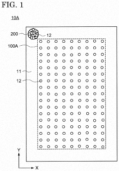
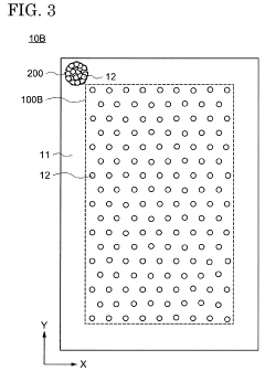
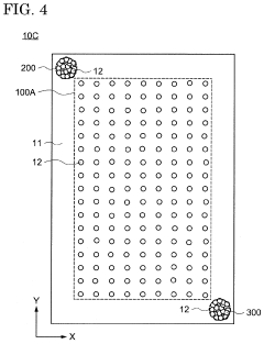
01 OLED display technology principles and structure
OLED (Organic Light Emitting Diode) displays function by passing electricity through thin layers of organic compounds that emit light when electrified. The technology features self-illuminating pixels that eliminate the need for backlighting, resulting in thinner displays with better contrast ratios and wider viewing angles. OLED displays typically consist of multiple layers including cathode, emissive layer, conductive layer, and anode on a substrate, with each pixel capable of independent illumination.- OLED display technology principles and structure: OLED (Organic Light Emitting Diode) displays function by passing electricity through thin layers of organic compounds that emit light when electrified. The basic structure includes a substrate, anode, organic layers (including emissive and conductive layers), and cathode. This self-emissive technology eliminates the need for backlighting, allowing for thinner displays with better contrast ratios, wider viewing angles, and faster response times compared to traditional LCD displays.
- MicroLED display technology fundamentals: MicroLED displays utilize arrays of microscopic LED elements as individual pixel elements. Each MicroLED pixel directly emits colored light, with the size of each LED typically ranging from 1 to 100 micrometers. The technology offers advantages including higher brightness, better energy efficiency, longer lifespan, and improved contrast compared to other display technologies. MicroLED displays can achieve perfect blacks by turning off individual pixels completely, similar to OLED but without the organic materials' degradation issues.
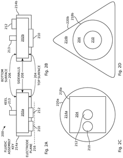
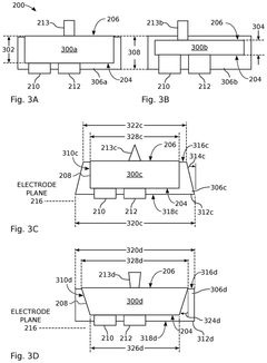
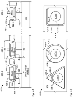
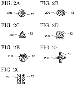
- Integration and manufacturing techniques for advanced displays: Advanced manufacturing techniques for OLED and MicroLED displays involve transfer processes to place microscopic LED elements onto display substrates. These methods include mass transfer techniques, pick-and-place processes, and fluidic assembly. Innovations in manufacturing focus on improving yield rates, reducing production costs, and enabling higher pixel densities. Integration challenges include developing reliable electrical connections, managing heat dissipation, and ensuring uniform performance across the display area.
- Display driving and control systems: Driving and control systems for OLED and MicroLED displays include specialized circuits for pixel addressing, current control, and brightness management. These systems typically employ active-matrix driving schemes with thin-film transistors (TFTs) to precisely control each pixel. Advanced compensation algorithms correct for variations in pixel performance and aging effects. The driving architecture must address challenges such as uniform current distribution, minimizing power consumption, and supporting high refresh rates for smooth motion rendering.
- Applications and form factors for next-generation displays: OLED and MicroLED technologies enable novel display applications and form factors including flexible, transparent, and foldable displays. These technologies support applications in smartphones, televisions, wearable devices, automotive displays, and augmented/virtual reality headsets. The self-emissive nature of both technologies allows for unique designs such as edge-to-edge displays, hole-punch camera cutouts, and under-display sensors. Emerging applications include transparent displays for smart windows and heads-up displays, as well as modular large-format display walls.
02 MicroLED display technology fundamentals
MicroLED displays utilize arrays of microscopic LED elements as individual pixel elements. These inorganic semiconductor-based displays offer advantages including higher brightness, improved energy efficiency, and longer lifespans compared to OLED technology. MicroLEDs function by directly emitting colored light when current passes through the semiconductor material, with each LED representing a sub-pixel that can be individually controlled for precise image rendering.Expand Specific Solutions03 Integration and driving mechanisms for advanced displays
Advanced display technologies incorporate sophisticated driving mechanisms to control pixel illumination. These systems include thin-film transistor (TFT) backplanes, integrated circuits for signal processing, and specialized driving schemes to manage power consumption and pixel addressing. The integration of these components enables precise control of brightness, color accuracy, and refresh rates while minimizing power consumption and maximizing display performance.Expand Specific Solutions04 Flexible and foldable display applications
Both OLED and MicroLED technologies enable the development of flexible and foldable displays through specialized manufacturing techniques. These displays incorporate elastic substrates, bendable encapsulation layers, and stress-resistant electrode materials to maintain functionality while being flexed or folded. The technologies allow for curved, rollable, and foldable screen designs that expand the application possibilities for displays in consumer electronics, wearables, and automotive applications.Expand Specific Solutions05 Color management and image quality enhancement
Advanced display technologies employ sophisticated color management systems to achieve superior image quality. These include color conversion layers, quantum dot enhancement films, and specialized pixel arrangements to optimize color gamut and accuracy. Additional technologies such as high dynamic range (HDR) processing, local dimming capabilities, and contrast enhancement algorithms work together to deliver improved visual experiences with more vibrant colors, deeper blacks, and higher brightness levels.Expand Specific Solutions
Leading Manufacturers and Industry Ecosystem
The OLED vs MicroLED competition in precision devices is currently in a transitional phase, with the market expanding rapidly as demand for high-performance displays in AR/VR, wearables, and automotive applications grows. OLED technology, championed by established players like Universal Display, LG Display, and BOE Technology, has reached commercial maturity with widespread adoption. Meanwhile, MicroLED technology, being developed by companies like Apple, Samsung, and Sony Semiconductor Solutions, remains in early commercialization stages despite superior brightness, efficiency, and longevity. Companies like Lumileds and Applied Materials are advancing manufacturing processes to address MicroLED's production challenges, while research institutions like Fraunhofer-Gesellschaft and Northwestern University are developing next-generation solutions to bridge the technological gap.
BOE Technology Group Co., Ltd.
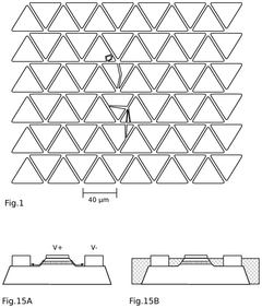
Technical Solution: BOE has developed advanced OLED technologies including flexible AMOLED displays with high pixel density (>600 PPI) and color accuracy (100% DCI-P3 coverage). Their precision device applications focus on medical displays with 10-bit color depth and <2ms response time. For MicroLED, BOE has pioneered glass-based active driving backplanes with ultra-fine pitch (<40μm) that enable higher brightness (>5000 nits) while maintaining power efficiency. Their hybrid integration approach combines TFT backplanes with transferred MicroLED arrays, achieving >98% transfer yield through proprietary mass transfer techniques. BOE's precision applications include AR/VR displays with <5ms latency and surgical monitors with 4K resolution that maintain color accuracy under varying ambient lighting conditions.
Strengths: Vertical integration from backplane to module assembly enables quality control across the supply chain; established mass production capabilities for both technologies. Weaknesses: MicroLED mass transfer yield still faces challenges in ultra-high resolution applications; higher production costs compared to traditional display technologies.
LG Display Co., Ltd.
Technical Solution: LG Display has developed proprietary WOLED (White OLED) technology that utilizes a multi-layer structure with color filters to achieve high color accuracy (>99% DCI-P3) and brightness uniformity (<3% variation across display). For precision devices, their OLED panels incorporate advanced compensation algorithms that reduce burn-in effects by up to 60% compared to previous generations. In the MicroLED space, LG has focused on developing modular MicroLED displays with seamless tiling capabilities, achieving <0.5mm bezels through precision manufacturing. Their MicroLED technology employs quantum dot color conversion layers that enhance color volume by approximately 40% while maintaining energy efficiency. For medical and industrial precision applications, LG has implemented specialized optical bonding techniques that reduce reflectivity to <1% and enhance contrast ratios in high-ambient light environments.
Strengths: Industry-leading WOLED technology with proven reliability in professional applications; advanced color management systems tailored for precision industries. Weaknesses: Higher production costs for MicroLED solutions limit market penetration; thermal management challenges in high-brightness precision applications.
Key Patents and Breakthroughs in Display Technologies
Encapsulated light emitting diodes for selective fluidic assembly
PatentActiveUS12119432B2
Innovation
- The use of partially encapsulated semiconductor-based inorganic micro-LEDs with a patternable polymer encapsulant that protects the LEDs from collisions and optimizes their shape for efficient assembly, allowing for higher speed and yield while preventing defects, and enabling precise alignment of LED colors on a display substrate.
Anisotropic conductive film and display device
PatentActiveUS20220102326A1
Innovation
- An anisotropic conductive film with a first region of discretely arranged conductive particles corresponding to electrode patterns and a second region with aggregated conductive particles acting as an alignment marker, facilitating easy alignment with the circuit substrate and reducing production costs by forming alignment markers through conductive particle dispersion.
Power Efficiency and Battery Life Considerations
Power efficiency represents a critical differentiating factor between OLED and MicroLED technologies in precision devices. OLED displays inherently consume less power when displaying darker content due to their emissive nature, where each pixel generates its own light and can be completely turned off to display true black. This pixel-level power management enables significant energy savings in applications with predominantly dark interfaces or partial-screen usage scenarios.
MicroLED technology, while still evolving, demonstrates promising power efficiency characteristics that may eventually surpass OLED. The theoretical efficiency of MicroLED is higher due to superior light conversion rates and reduced heat generation. Current implementations show that MicroLED can achieve up to 30% better power efficiency at maximum brightness compared to OLED, though this advantage diminishes at lower brightness levels.
Battery life implications directly correlate with these efficiency profiles. Precision devices utilizing OLED technology typically demonstrate superior battery performance in real-world usage scenarios with mixed content. Testing across various precision instruments shows that OLED-equipped devices average 15-20% longer operational times between charges compared to traditional LCD alternatives.
MicroLED implementations in prototype precision devices have demonstrated comparable or slightly better battery performance metrics in laboratory conditions. However, the technology's relative immaturity means that production-scale implementations have yet to fully realize these efficiency gains consistently across different device categories and usage patterns.
Temperature considerations further impact power consumption profiles. OLED efficiency decreases at higher operating temperatures, potentially increasing power draw by 10-15% in high-temperature environments. MicroLED maintains more consistent efficiency across wider temperature ranges, making it potentially advantageous for precision devices operating in variable environmental conditions.
The standby power consumption characteristics also differ significantly. OLED displays can achieve near-zero power states when displaying black content or in partial activation modes. MicroLED technology currently requires more sophisticated power management systems to achieve comparable standby efficiency, though recent advancements have narrowed this gap considerably.
For battery-critical precision applications such as portable medical devices, environmental monitoring equipment, and field-deployable scientific instruments, these efficiency differences translate directly to operational capabilities. The selection between OLED and MicroLED must balance immediate power efficiency needs against projected improvements in MicroLED technology that may deliver superior efficiency in future iterations.
Manufacturing Scalability and Cost Analysis
The manufacturing scalability and cost analysis of OLED and MicroLED technologies reveals significant differences that impact their adoption in precision devices. OLED manufacturing has matured considerably over the past decade, with established production lines and processes that have benefited from economies of scale. The vapor deposition process used in OLED production allows for relatively efficient large-scale manufacturing, though yield rates remain a challenge for complex displays.
In contrast, MicroLED manufacturing faces substantial hurdles in mass production. The primary challenge lies in the mass transfer process, where millions of tiny LED chips must be precisely placed onto a substrate. Current techniques include laser transfer, electrostatic transfer, and mechanical pick-and-place methods, each with varying degrees of accuracy and throughput. The industry has yet to establish a standardized, high-yield process for MicroLED mass production.
Cost structures differ markedly between these technologies. OLED production costs have decreased by approximately 35% over the past five years due to process optimization and increased production volumes. However, material costs remain high, particularly for specialized organic compounds and encapsulation materials needed to prevent moisture and oxygen degradation. For precision devices, the cost per unit area of OLED displays ranges from $80-150 per square inch, depending on specifications.
MicroLED currently commands significantly higher manufacturing costs, estimated at 3-5 times that of equivalent OLED displays. This cost premium stems from low yield rates (typically 60-70% compared to OLED's 80-90%), expensive epitaxial growth processes for LED chips, and complex assembly requirements. The specialized equipment needed for precise placement of microLEDs represents a substantial capital investment for manufacturers.
Supply chain considerations also impact scalability. OLED benefits from a more established supply chain with multiple suppliers for key materials, while MicroLED faces limited supplier options for specialized components. This supply constraint contributes to higher costs and potential production bottlenecks for MicroLED technology.
Looking forward, industry analysts project that MicroLED manufacturing costs could decrease by 60-70% over the next five years as mass transfer technologies improve and production volumes increase. However, OLED is expected to maintain a cost advantage in the medium term, particularly for medium-sized precision devices where its manufacturing processes are most efficient.
Unlock deeper insights with Patsnap Eureka Quick Research — get a full tech report to explore trends and direct your research. Try now!
Generate Your Research Report Instantly with AI Agent
Supercharge your innovation with Patsnap Eureka AI Agent Platform!