

OLED vs MicroLED: Standards Governing Manufacture
OCT 24, 20259 MIN READ
Generate Your Research Report Instantly with AI Agent
PatSnap Eureka helps you evaluate technical feasibility & market potential.
Display Technology Evolution and Objectives
The evolution of display technology has witnessed significant transformations over the past decades, from cathode ray tubes (CRTs) to liquid crystal displays (LCDs), and more recently to organic light-emitting diodes (OLEDs). Each transition has brought improvements in visual quality, energy efficiency, and form factor flexibility. Currently, the industry stands at another pivotal juncture with the emergence of MicroLED technology, promising to overcome certain limitations of OLED displays.
OLED technology, which gained commercial prominence in the early 2000s, revolutionized displays by eliminating the need for backlighting, thereby enabling thinner screens with superior contrast ratios and more vibrant colors. The self-emissive nature of OLEDs allows for perfect blacks and exceptional viewing angles, making them ideal for premium smartphones, televisions, and wearable devices.
MicroLED represents the next frontier in display technology, utilizing microscopic LED arrays that are self-emissive like OLEDs but offer potential advantages in brightness, longevity, and energy efficiency. Unlike OLEDs, which use organic compounds susceptible to degradation over time, MicroLEDs employ inorganic materials that promise extended lifespans and resistance to burn-in effects.
The technical objectives driving the development of both OLED and MicroLED technologies include achieving higher pixel densities, reducing power consumption, enhancing color accuracy, and improving manufacturing yields. For OLEDs, addressing issues of blue pixel degradation and extending overall panel lifespan remain critical goals. MicroLED development focuses on overcoming mass transfer challenges and reducing production costs to enable broader market adoption.
Industry standards governing the manufacture of these advanced display technologies are evolving to address quality control, environmental impact, and performance metrics. Organizations such as the International Electrotechnical Commission (IEC) and the Society for Information Display (SID) are working to establish standardized testing protocols and specifications for both OLED and MicroLED manufacturing processes.
The trajectory of display technology evolution suggests a future where MicroLED may eventually supplant OLED in certain applications, particularly those requiring extreme brightness or longevity. However, the transition will likely be gradual, with OLED continuing to dominate in the near term due to established manufacturing infrastructure and ongoing innovations in materials science.
Understanding the technical foundations, manufacturing challenges, and standardization efforts for both OLED and MicroLED technologies is essential for anticipating market developments and identifying strategic opportunities in the evolving display landscape.
Market Demand Analysis for Advanced Display Technologies
The display technology market is witnessing unprecedented growth driven by increasing consumer demand for superior visual experiences across multiple devices. Current market analysis indicates that the global advanced display market is projected to reach $167 billion by 2025, with OLED technology currently dominating premium segments while MicroLED emerges as a promising contender. This growth trajectory is supported by expanding applications in smartphones, televisions, wearables, automotive displays, and commercial signage.
Consumer preferences are shifting decisively toward thinner, more energy-efficient displays with higher resolution, better color accuracy, and longer lifespans. OLED technology has established strong market penetration due to its superior contrast ratios, flexibility, and color reproduction capabilities. However, research indicates growing consumer awareness of OLED limitations regarding brightness levels and potential screen burn-in issues, creating market openings for alternative technologies.
MicroLED displays are generating significant market interest despite limited commercial availability. Industry surveys reveal that 78% of high-end consumers express willingness to pay premium prices for MicroLED benefits including superior brightness, energy efficiency, and longevity. The automotive sector particularly values MicroLED's performance under varying lighting conditions, with projected compound annual growth rate of 63% in this vertical through 2027.
Regional market analysis shows Asia-Pacific leading manufacturing capacity for both technologies, with South Korea and China making substantial investments in production facilities. North America and Europe represent primary consumption markets, with particularly strong demand in luxury consumer electronics and commercial applications where display quality directly impacts consumer experience and brand perception.
Supply chain considerations are increasingly influencing market dynamics. OLED manufacturing has achieved economies of scale, though production remains concentrated among few manufacturers. MicroLED faces significant supply chain challenges with mass transfer processes representing a critical bottleneck. Market research indicates that manufacturing standardization could reduce MicroLED production costs by up to 40%, potentially accelerating market adoption.
Enterprise and institutional buyers are demonstrating growing interest in advanced display technologies, with particular emphasis on total cost of ownership calculations that favor longer-lasting technologies. Healthcare, military, aerospace, and high-end retail sectors are emerging as significant early adopters of MicroLED technology despite premium pricing, driven by specific performance requirements that OLED cannot fully address.
OLED and MicroLED Manufacturing Standards Landscape
The manufacturing standards landscape for OLED and MicroLED technologies represents a complex ecosystem of regulations, industry specifications, and quality control frameworks that govern production processes across global markets. These standards serve as critical benchmarks for ensuring consistency, reliability, and safety in display manufacturing.
For OLED manufacturing, the International Electrotechnical Commission (IEC) has established several key standards, including IEC 62341 series which specifically addresses organic light-emitting diode displays. These standards cover essential aspects such as measurement methods, reliability testing protocols, and environmental considerations. Additionally, the Society for Information Display (SID) has developed industry-specific guidelines that focus on performance metrics and quality assessment methodologies.
MicroLED manufacturing, being a relatively newer technology, has fewer established dedicated standards. However, it largely operates under broader semiconductor and display manufacturing frameworks such as those provided by SEMI (Semiconductor Equipment and Materials International). The SEMI MS series standards are particularly relevant for microelectronic manufacturing processes applicable to MicroLED production.
Both technologies must comply with regional regulatory frameworks that vary significantly across major manufacturing hubs. In Asia, particularly in South Korea, Japan, and Taiwan, local standards organizations have developed specialized protocols that complement international standards while addressing region-specific manufacturing considerations. The Korean Agency for Technology and Standards (KATS) and Japan Electronics and Information Technology Industries Association (JEITA) have been particularly active in this domain.
Environmental compliance standards represent another critical dimension of the manufacturing landscape. The EU's Restriction of Hazardous Substances (RoHS) directive and Registration, Evaluation, Authorization and Restriction of Chemicals (REACH) regulations significantly impact material selection and processing methods for both OLED and MicroLED manufacturers. Similarly, energy efficiency standards such as Energy Star influence design parameters and production specifications.
Quality management systems standards like ISO 9001 provide overarching frameworks for manufacturing excellence, while more specialized standards such as ISO 14644 for cleanroom environments directly impact production facility requirements. These standards are particularly crucial for MicroLED manufacturing, which demands extremely high levels of cleanliness and contamination control.
Emerging standards are beginning to address novel aspects of next-generation display manufacturing, including quantum dot integration, flexible display production, and advanced encapsulation techniques. Organizations such as the International Committee for Display Metrology (ICDM) are working to develop measurement standards that can accurately characterize the unique properties of these advanced display technologies.
Current Manufacturing Compliance Frameworks
01 OLED manufacturing processes and quality standards
Manufacturing processes for OLED displays involve specific techniques to ensure quality and performance standards. These processes include deposition methods for organic materials, electrode formation, and encapsulation techniques to protect the sensitive organic layers from environmental factors. Quality control standards focus on uniformity of light emission, color accuracy, and prevention of pixel defects. Advanced manufacturing standards also address issues of production efficiency and yield improvement.- OLED manufacturing techniques and materials: Various manufacturing techniques and materials are used in OLED display production to enhance performance and efficiency. These include specialized deposition methods for organic layers, electrode materials optimization, and encapsulation techniques to protect against environmental degradation. Advanced manufacturing standards focus on achieving uniform light emission, improving color accuracy, and extending device lifespan through precise control of material properties and processing conditions.
- MicroLED fabrication and integration methods: MicroLED display manufacturing involves specialized fabrication and integration methods to achieve high-resolution displays with superior brightness and efficiency. Key manufacturing standards address the challenges of mass transfer techniques for positioning microscopic LED elements, electrical interconnection methods, and substrate preparation. These standards ensure consistent pixel performance, color uniformity, and structural integrity across large display areas.
- Quality control and testing standards: Manufacturing standards for both OLED and MicroLED displays include comprehensive quality control and testing protocols. These standards specify methods for evaluating display uniformity, brightness, color accuracy, contrast ratio, and viewing angle performance. Advanced testing procedures also address reliability factors such as thermal stability, humidity resistance, and operational lifetime under various conditions to ensure consistent product quality and performance.
- Substrate and backplane technology standards: Manufacturing standards for display substrates and backplane technologies are critical for both OLED and MicroLED displays. These standards address requirements for substrate materials, thin-film transistor (TFT) designs, and circuit integration methods. Key considerations include thermal stability, mechanical flexibility, electrical performance, and compatibility with subsequent manufacturing processes to ensure reliable display operation and longevity.
- Environmental and efficiency standards: Manufacturing standards for OLED and MicroLED displays increasingly focus on environmental sustainability and energy efficiency. These standards address power consumption optimization, materials selection for reduced environmental impact, and manufacturing process efficiency. Requirements include minimizing hazardous substances, improving resource utilization, reducing waste generation, and enhancing energy efficiency during both production and operation of display devices.
02 MicroLED fabrication techniques and standards
MicroLED display manufacturing requires precise fabrication techniques to handle the miniaturized LED components. Standards focus on the transfer and placement accuracy of microscopic LED elements onto display substrates. Manufacturing processes include epitaxial growth of LED structures, wafer processing, and mass transfer techniques. Quality standards address issues of pixel uniformity, defect rates, and integration density to ensure high-resolution display performance.Expand Specific Solutions03 Substrate and backplane technology standards
Both OLED and MicroLED displays require specific standards for substrate materials and backplane technologies. Manufacturing standards address the requirements for thin-film transistor (TFT) backplanes, including stability, uniformity, and electrical performance. Substrate standards focus on material properties such as transparency, thermal stability, and mechanical flexibility. These standards ensure proper integration with the display elements and reliable operation under various conditions.Expand Specific Solutions04 Testing and quality assurance protocols
Manufacturing standards for OLED and MicroLED displays include comprehensive testing and quality assurance protocols. These standards define methods for measuring display performance parameters such as brightness, contrast ratio, color gamut, and viewing angle. Testing procedures also address reliability factors including lifetime testing, environmental stress testing, and accelerated aging tests. Quality assurance standards ensure consistency across production batches and compliance with industry specifications.Expand Specific Solutions05 Materials purity and handling standards
Manufacturing standards for display technologies specify requirements for materials purity and handling procedures. For OLEDs, standards address the purity levels of organic compounds and methods to prevent contamination during processing. MicroLED standards focus on semiconductor material quality and handling of microscopic components. Both technologies require clean room environments with specific particulate control standards. Material handling protocols ensure consistency in device performance and manufacturing yield.Expand Specific Solutions
Key Industry Players and Standards Organizations
The OLED vs MicroLED display technology landscape is currently in a transitional phase, with OLED being mature and widely commercialized while MicroLED remains in early commercialization stages. The global market for these advanced display technologies is projected to exceed $200 billion by 2025, driven by demand for higher performance displays in consumer electronics and automotive applications. In terms of technical maturity, established players like Samsung Electronics, BOE Technology, and LG Display have achieved mass production capabilities for OLED, while MicroLED faces manufacturing challenges being addressed by companies like eLux and Applied Materials. Emerging players such as Lumileds and Guangzhou New Vision are developing innovative manufacturing processes to overcome MicroLED's complex assembly requirements, particularly in mass transfer techniques and yield management, which remain key barriers to widespread adoption.
BOE Technology Group Co., Ltd.
Technical Solution: BOE has developed comprehensive manufacturing standards for both OLED and MicroLED technologies. For OLED, BOE implements strict quality control protocols focusing on thin-film transistor (TFT) backplane uniformity and organic material deposition precision. Their OLED manufacturing follows ISO 9001:2015 quality management systems and incorporates proprietary evaporation techniques that achieve ±2.5% thickness uniformity across large substrates. For MicroLED, BOE has pioneered mass transfer processes with positioning accuracy of <1μm, critical for high-resolution displays. Their manufacturing standards include specialized testing protocols for individual LED dies before transfer, achieving defect rates below 1 per million. BOE has also established environmental standards exceeding industry requirements, with clean room specifications at ISO Class 3 (less than 1,000 particles ≥0.1μm per cubic meter) for their advanced display manufacturing facilities.
Strengths: BOE's vertical integration allows for comprehensive quality control across the entire manufacturing process. Their established OLED production lines provide economies of scale and manufacturing expertise that transfers to MicroLED development. Weaknesses: BOE's MicroLED mass transfer technology still faces yield challenges at commercial scale, with higher defect rates than their mature OLED processes, resulting in higher production costs for MicroLED displays.
Wuhan China Star Optoelectronics Technology Co., Ltd.
Technical Solution: Wuhan China Star Optoelectronics Technology (CSOT) has developed distinct manufacturing standards for both OLED and MicroLED production. For OLED, CSOT implements rigorous quality control systems following ISO 9001:2015 and specialized display industry standards like SID Display Measurement Standards. Their OLED manufacturing incorporates advanced vapor deposition techniques achieving organic layer uniformity within ±3% across Gen 6 substrates. CSOT's OLED production lines maintain clean room environments at ISO Class 4 or better, with temperature stability of ±0.5°C and humidity control within ±3%. For MicroLED development, CSOT has established proprietary standards for mass transfer processes, achieving placement accuracy of approximately 1.5μm for RGB MicroLED chips. Their quality assurance protocols include automated optical inspection systems that can detect defects down to 2μm in size, with specialized testing for both electrical and optical performance of individual MicroLED elements before and after transfer to the display substrate.
Strengths: CSOT benefits from strong backing by TCL Corporation, providing financial resources for advanced manufacturing equipment and R&D. Their established OLED production experience provides valuable expertise in thin-film processes applicable to MicroLED development. Weaknesses: CSOT's MicroLED manufacturing technology remains less mature than their OLED capabilities, with current mass transfer processes showing lower yields and higher defect rates, particularly for ultra-high resolution applications requiring sub-micron placement accuracy.
Critical Patents and Technical Specifications
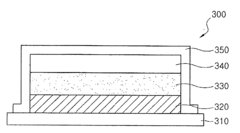
Organic light-emitting diode device and manufacturing method thereof
PatentInactiveEP2182563A3
Innovation
- The OLED device incorporates multiple light emitting layers, with one layer emitting bluer light near the anode and another emitting redder light near the cathode, allowing color temperature adjustment through input voltage without additional circuitry, utilizing a structure that includes hole transporting, electron transporting, and blocking layers, and electron injection layers.
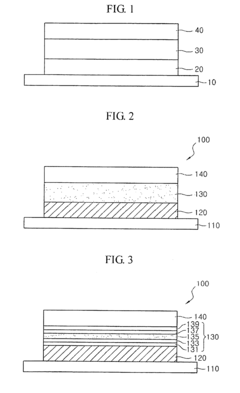
Organic light emitting diode and method for manufacturing the same
PatentInactiveUS20090167169A1
Innovation
- A method for manufacturing OLEDs using a metal paste to form electrodes, which simplifies the process, reduces contaminant discharge, and lowers costs by eliminating the need for additional patterning, incorporating a heat-treatment of the metal paste and the use of transparent conductive oxides for electrodes, along with inorganic and organic thin films.
Environmental Compliance Requirements
Environmental compliance has become a critical factor in the manufacturing standards for both OLED and MicroLED display technologies. As regulatory frameworks evolve globally, manufacturers must navigate increasingly stringent requirements aimed at reducing environmental impact throughout the product lifecycle.
For OLED manufacturing, the primary environmental concerns center around the use of organic solvents and heavy metals. The EU's Restriction of Hazardous Substances (RoHS) directive strictly limits the use of lead, mercury, cadmium, and other toxic substances in electronic displays. OLED producers must comply with these restrictions while maintaining product performance. Additionally, many OLED manufacturing processes involve fluorinated greenhouse gases (F-gases) which are regulated under the Kyoto Protocol and subsequent climate agreements.
MicroLED manufacturing faces different environmental challenges, particularly related to the gallium nitride (GaN) substrates commonly used. The extraction and processing of rare earth elements required for MicroLED production are subject to mining regulations and sustainability reporting requirements in various jurisdictions. Unlike OLEDs, MicroLEDs typically contain fewer organic compounds but may involve more complex semiconductor fabrication processes with their own environmental compliance needs.
Both technologies must adhere to energy efficiency standards during manufacturing. The ISO 50001 energy management standard has been widely adopted across the display industry, requiring manufacturers to implement systematic approaches to energy consumption reduction. In regions like California and the European Union, specific energy efficiency requirements for display manufacturing facilities add another layer of compliance complexity.
Waste management represents another significant area of environmental regulation. OLED manufacturing generates organic waste streams that may be classified as hazardous in certain jurisdictions, while MicroLED production creates semiconductor waste requiring specialized disposal protocols. The Basel Convention on hazardous waste movement across borders impacts global supply chains for both technologies.
Water usage and contamination controls are increasingly important, with semiconductor fabrication facilities facing strict limits on water consumption and discharge quality. MicroLED manufacturing typically requires ultra-pure water in greater volumes than OLED production, making water recycling technologies essential for compliance in water-stressed regions.
Looking forward, emerging regulations around carbon footprinting and lifecycle assessment are likely to impact both technologies. The EU's Carbon Border Adjustment Mechanism and similar policies being developed in other regions will require manufacturers to account for embedded carbon in display technologies, potentially creating competitive advantages for the more energy-efficient manufacturing processes.
Supply Chain Quality Assurance Standards
Quality assurance standards across the supply chain represent a critical framework for both OLED and MicroLED manufacturing processes. These standards ensure consistency, reliability, and performance of the final display products while minimizing defects and waste throughout the production lifecycle.
For OLED manufacturing, the supply chain quality assurance typically follows ISO 9001 quality management systems as the foundational standard. Additionally, specialized standards like IEC 62341 series specifically address organic light-emitting diode displays, providing detailed requirements for quality control during material sourcing, panel production, and final assembly. Major OLED manufacturers have implemented strict supplier certification programs that require upstream material providers to meet stringent purity levels for organic compounds, with contamination tolerances often measured in parts per billion.
MicroLED manufacturing, being a newer technology, has fewer established industry-specific standards but relies heavily on semiconductor manufacturing standards like SEMI (Semiconductor Equipment and Materials International) guidelines. These standards govern the quality of epitaxial wafers, LED chip production, and transfer processes. The JEDEC solid-state technology association has also begun developing standards specifically addressing microLED reliability and performance characteristics.
Both technologies require comprehensive traceability systems throughout their supply chains. For OLED, this includes tracking organic material batches from synthesis to deposition, while MicroLED demands meticulous tracking of individual LED chips from wafer fabrication through to the mass transfer process. These traceability requirements are often codified in standards like ISO 13485 (borrowed from medical device manufacturing) to ensure complete documentation of all components.
Environmental compliance standards also play a significant role in supply chain quality assurance. RoHS (Restriction of Hazardous Substances) and REACH (Registration, Evaluation, Authorization and Restriction of Chemicals) regulations impose strict limitations on materials used in both technologies, requiring manufacturers to implement rigorous supplier verification protocols and material testing regimes.
Emerging quality assurance trends include the development of AI-powered inspection systems that can detect defects at earlier stages in the supply chain. These systems are gradually being incorporated into standards requirements, particularly for high-volume production environments. Additionally, industry consortiums like the International Committee for Display Metrology (ICDM) are working to standardize testing methodologies specific to next-generation display technologies, ensuring consistent quality metrics across different manufacturers and supply chain partners.
Unlock deeper insights with PatSnap Eureka Quick Research — get a full tech report to explore trends and direct your research. Try now!
Generate Your Research Report Instantly with AI Agent
Supercharge your innovation with PatSnap Eureka AI Agent Platform!