How OLED vs MicroLED Nurture the Growth of Display Innovation
OCT 24, 202510 MIN READ
Generate Your Research Report Instantly with AI Agent
Patsnap Eureka helps you evaluate technical feasibility & market potential.
OLED and MicroLED Display Technology Evolution
The evolution of display technology has witnessed significant milestones over the past decades, with OLED (Organic Light-Emitting Diode) and MicroLED emerging as revolutionary technologies that have fundamentally transformed visual experiences. OLED technology, first conceptualized in the 1970s and commercialized in the late 1990s, represented a paradigm shift from traditional LCD displays by eliminating the need for backlighting, enabling thinner form factors, and delivering superior contrast ratios.
The technological trajectory of OLED has progressed through several generations, beginning with passive-matrix OLED (PMOLED) displays, which were suitable for small screens with limited resolution. The subsequent development of active-matrix OLED (AMOLED) technology in the early 2000s marked a significant advancement, enabling higher resolution, improved power efficiency, and enhanced response times, making it viable for smartphones and larger displays.
MicroLED technology, while conceptualized earlier, has gained substantial momentum in the past decade. Unlike OLED, which uses organic compounds that emit light when electricity is applied, MicroLED utilizes microscopic inorganic LED arrays. This fundamental difference addresses several limitations of OLED, including burn-in issues and lifespan concerns, while potentially offering even better contrast, brightness, and energy efficiency.
The technological evolution of these display technologies has been characterized by continuous improvements in manufacturing processes. For OLED, key advancements include the transition from evaporation-based deposition to solution-based processing, the development of flexible and foldable OLED panels, and the integration of quantum dot technology to enhance color gamut and efficiency (QD-OLED).
MicroLED's evolution has focused on overcoming critical manufacturing challenges, particularly in mass transfer techniques required to place millions of microscopic LEDs precisely on substrates. Innovations in pick-and-place technologies, self-assembly methods, and photolithographic approaches have gradually improved yield rates and reduced production costs, though mass production remains challenging.
Both technologies have converged on similar innovation paths regarding pixel density improvements, color accuracy enhancements, and power efficiency optimization. The pursuit of higher resolution displays has driven pixel sizes down to microscopic levels, with OLED achieving sub-pixel dimensions below 50 micrometers and MicroLED pushing boundaries even further with LED chips approaching 3-10 micrometers.
Recent technological trends indicate a potential hybridization approach, where manufacturers leverage the strengths of both technologies. Samsung's Neo QLED and LG's QNED displays represent intermediate steps that incorporate mini-LED backlighting (a precursor to MicroLED) with quantum dot technology, bridging the gap between conventional displays and future MicroLED implementations.
The evolution continues with research focusing on transparent displays, stretchable form factors, and integration with advanced AI processing to optimize visual performance based on content and viewing conditions, setting the stage for the next generation of immersive visual experiences.
Market Demand Analysis for Advanced Display Technologies
The display technology market has witnessed significant growth in recent years, driven by increasing consumer demand for superior visual experiences across various devices. OLED (Organic Light Emitting Diode) technology has dominated premium segments, while MicroLED emerges as a promising next-generation alternative. Current market analysis indicates the global advanced display market reached approximately $143 billion in 2022, with projections suggesting growth to $206 billion by 2027, representing a compound annual growth rate of 7.6%.
Consumer electronics remains the primary demand driver, with smartphones accounting for nearly 40% of advanced display implementations. High-end television segments have shown particularly strong adoption rates for OLED technology, with annual growth exceeding 20% in premium price brackets. Meanwhile, wearable devices represent the fastest-growing segment, with display requirements emphasizing power efficiency and form factor flexibility.
Market research indicates shifting consumer preferences toward displays offering higher resolution, improved color accuracy, and reduced power consumption. Surveys reveal that 78% of smartphone users consider display quality among their top three purchase decision factors, while 65% of television buyers prioritize picture quality above other features. This trend has accelerated the transition from LCD to OLED in premium device categories.
Commercial applications present substantial growth opportunities, particularly in automotive displays, retail signage, and healthcare monitoring systems. The automotive display market alone is projected to grow at 12.3% annually through 2028, driven by increasing dashboard digitization and infotainment system integration. These sectors demand displays with exceptional durability, brightness, and operational longevity—attributes where MicroLED technology demonstrates particular promise.
Regional analysis reveals Asia-Pacific as the dominant manufacturing hub, accounting for over 60% of global display production capacity. However, North America and Europe lead in premium segment consumption and technology innovation investment. China has emerged as both a major production center and consumption market, with domestic manufacturers rapidly advancing their technological capabilities.
Supply chain considerations significantly impact market dynamics, with recent component shortages highlighting vulnerabilities in the display industry. Material constraints, particularly for rare earth elements used in phosphors and semiconductor materials, have created production bottlenecks affecting both OLED and MicroLED development. These constraints have accelerated research into alternative materials and manufacturing processes to ensure sustainable industry growth.
The competitive landscape shows increasing consolidation among display manufacturers, with vertical integration becoming a prevalent strategy. Companies controlling both panel production and device manufacturing demonstrate stronger market resilience and innovation capacity, particularly in developing proprietary display technologies that differentiate their product offerings.
Current Technical Challenges in OLED and MicroLED Development
Despite significant advancements in display technologies, both OLED and MicroLED face substantial technical challenges that impede their widespread adoption and further innovation. OLED technology continues to struggle with limited lifetime issues, particularly for blue emitters which degrade faster than red and green counterparts. This differential aging leads to color shift over time, compromising display quality and consistency. Additionally, OLED panels remain susceptible to burn-in effects when static images are displayed for extended periods, a critical concern for commercial applications.
Manufacturing scalability presents another major hurdle for OLED, especially for larger displays where yield rates decline significantly. The complex vapor deposition processes required for OLED production demand extremely precise control over manufacturing conditions, increasing production costs and limiting accessibility for mass-market applications.
MicroLED technology faces even more formidable manufacturing challenges. The mass transfer process—moving millions of microscopic LED chips from growth substrates to display backplanes with perfect precision—remains the industry's most significant bottleneck. Current pick-and-place technologies struggle to achieve the necessary throughput while maintaining acceptable yield rates, particularly as pixel densities increase for higher resolution displays.
Color consistency across MicroLED panels represents another critical challenge. The varying efficiency of different colored LEDs necessitates sophisticated compensation algorithms and precise manufacturing control to ensure uniform brightness and color reproduction across the entire display surface. This becomes increasingly difficult as display sizes grow and pixel densities increase.
Both technologies confront power efficiency limitations, though in different ways. OLED displays require complex thin-film transistor backplanes that introduce power losses, while MicroLED systems need sophisticated driving circuits to manage the thousands or millions of individual LED elements. For mobile and wearable applications, these power constraints significantly impact device design and battery life.
Cost factors remain perhaps the most prohibitive barrier to widespread adoption, particularly for MicroLED. Current manufacturing processes for MicroLED displays can be 5-10 times more expensive than equivalent OLED panels, limiting their market penetration to premium products and specialized applications. While OLED has achieved greater cost efficiency through years of manufacturing optimization, it still commands a significant premium over conventional LCD technology.
Material science limitations affect both technologies as well. OLED researchers continue searching for more stable organic compounds that can deliver improved lifetime without sacrificing color quality or efficiency. MicroLED developers face challenges in developing efficient, reliable epitaxial growth processes for the semiconductor materials used in the microscopic LED elements, particularly for achieving consistent quality at scale.
Comparative Analysis of OLED and MicroLED Solutions
01 OLED Display Technology Advancements
Organic Light Emitting Diode (OLED) technology has seen significant advancements in display innovation. These displays offer superior contrast ratios, wider viewing angles, and faster response times compared to traditional LCD displays. Recent innovations include flexible and foldable OLED panels, transparent displays, and improvements in energy efficiency. The technology utilizes organic compounds that emit light when an electric current is applied, eliminating the need for backlighting and allowing for thinner display profiles.- OLED display structure and materials innovation: Innovations in OLED display technology focus on improving the structure and materials used in these displays. This includes advancements in organic light-emitting materials, electrode configurations, and layer structures that enhance brightness, efficiency, and lifespan. These innovations address challenges such as power consumption and display degradation over time, while enabling thinner and more flexible display designs.
- MicroLED fabrication and integration techniques: MicroLED display technology involves innovative fabrication and integration methods for extremely small LED arrays. These techniques include advanced transfer processes for placing microscopic LEDs onto display substrates, novel interconnection methods, and integration with driving circuits. The innovations enable high-resolution displays with superior brightness, contrast ratios, and energy efficiency compared to traditional display technologies.
- Flexible and foldable display technologies: Innovations in flexible and foldable displays leverage both OLED and MicroLED technologies to create bendable, rollable, and foldable screens. These advancements include specialized substrate materials, encapsulation techniques, and mechanical designs that maintain display performance while enabling form factor flexibility. Such displays can be integrated into various devices including smartphones, wearables, and other consumer electronics.
- Display driving and control systems: Advanced driving and control systems for OLED and MicroLED displays focus on improving image quality, refresh rates, and power efficiency. These innovations include pixel driving circuits, backplane technologies, and control algorithms that enhance display performance. The systems address challenges such as uniform brightness, color accuracy, and response time while supporting high-resolution and high-dynamic-range content.
- Hybrid and multi-technology display solutions: Hybrid display solutions combine elements of OLED, MicroLED, and other display technologies to leverage the strengths of each. These innovations include multi-layer displays, hybrid pixel architectures, and complementary technology integration. Such approaches enable displays with enhanced performance characteristics including improved brightness, color gamut, power efficiency, and lifespan while overcoming limitations of single-technology solutions.
02 MicroLED Display Innovations
MicroLED technology represents the next generation of display innovation, offering significant improvements over both LCD and OLED technologies. These displays use microscopic LED arrays to create self-emissive pixels with exceptional brightness, contrast, and energy efficiency. Recent innovations focus on manufacturing processes to reduce production costs, improve yield rates, and enable mass production of high-resolution MicroLED displays for various applications including smartphones, televisions, and wearable devices.Expand Specific Solutions03 Hybrid and Integrated Display Solutions
Innovations in hybrid display technologies combine elements of OLED and MicroLED to leverage the advantages of both. These integrated solutions aim to overcome limitations of individual technologies while maintaining high performance. Developments include pixel architecture that incorporates both technologies on a single substrate, shared driving circuits, and novel manufacturing techniques that allow for cost-effective production of hybrid displays with enhanced visual performance, energy efficiency, and durability.Expand Specific Solutions04 Display Manufacturing and Fabrication Techniques
Advanced manufacturing and fabrication techniques are crucial for the evolution of both OLED and MicroLED displays. Innovations in this area include improved deposition methods for organic materials, transfer processes for MicroLED pixels, and novel encapsulation technologies to protect sensitive components. These advancements focus on increasing production efficiency, reducing defect rates, and enabling the fabrication of displays with higher resolution, better uniformity, and enhanced durability at competitive costs.Expand Specific Solutions05 Display Integration with Interactive Technologies
Modern display innovations extend beyond visual performance to include integration with interactive technologies. These developments incorporate touch sensing, biometric authentication, and gesture recognition directly into the display structure. By embedding sensors within the display layers, manufacturers can create seamless user interfaces without compromising display quality. This integration enables new applications in consumer electronics, automotive displays, and augmented reality devices while maintaining the visual advantages of OLED and MicroLED technologies.Expand Specific Solutions
Key Industry Players in Advanced Display Manufacturing
The OLED vs MicroLED display technology landscape is currently in a transitional phase, with OLED being more commercially mature while MicroLED represents the emerging frontier. The global display market is projected to reach $200 billion by 2025, driven by demand for higher resolution and energy-efficient displays. Leading players like Samsung Display, BOE Technology, and TCL China Star Optoelectronics have established OLED manufacturing capabilities, while companies such as Apple, Lumileds, and Rayleigh Vision Intelligence are investing heavily in MicroLED development. The technology maturity gap is evident as BOE and Samsung have mass-produced OLED displays, whereas MicroLED faces manufacturing challenges including mass transfer techniques and yield rates, though companies like Changchun Xida and Applied Materials are making significant advances in production equipment.
BOE Technology Group Co., Ltd.
Technical Solution: BOE has developed advanced OLED manufacturing techniques including flexible OLED production lines utilizing LTPO (Low-Temperature Polycrystalline Oxide) backplane technology, which enables variable refresh rates from 1Hz to 120Hz, reducing power consumption by up to 30% compared to conventional LTPS displays. Their OLED panels incorporate pixel compensation circuits that minimize screen burn-in and maintain color accuracy over extended usage periods. For MicroLED, BOE has pioneered active-matrix driving technology with integrated circuits directly on the glass substrate, allowing for higher pixel density and more precise control of thousands of individual MicroLEDs. Their glass-based transfer process achieves placement accuracy below 1μm, essential for high-resolution MicroLED displays. BOE has also developed hybrid RGB+Mini LED backlighting solutions as an intermediate technology, offering improved contrast ratios (1,000,000:1) and color performance while MicroLED manufacturing techniques mature.
Strengths: Massive production capacity across multiple display technologies; strong vertical integration from substrate manufacturing to module assembly; government backing supporting long-term R&D investments. Weaknesses: Still catching up to Samsung and LG in high-end OLED quality; MicroLED mass production capabilities remain limited by yield challenges and high costs.
Samsung Electronics Co., Ltd.
Technical Solution: Samsung has pioneered Quantum Dot OLED (QD-OLED) technology, which combines quantum dots with OLED to deliver superior color accuracy and brightness. Their QD-OLED panels utilize blue OLED as the light source and quantum dot color conversion layers to produce red and green colors, resulting in wider color gamut (over 90% of BT.2020) and improved energy efficiency. Samsung has also made significant progress in MicroLED development with their modular "The Wall" display technology, featuring micrometer-sized LEDs that are self-emissive and inorganic. These MicroLED displays achieve brightness levels exceeding 2,000 nits while maintaining perfect black levels and near-infinite contrast ratios. Samsung's dual-track approach allows them to leverage the immediate commercial viability of advanced OLED while positioning for the future transition to MicroLED as manufacturing costs decrease.
Strengths: Market leadership in both OLED and MicroLED technologies; vertical integration from component manufacturing to final display production; strong IP portfolio. Weaknesses: High production costs for MicroLED technology limiting mass market adoption; QD-OLED technology faces yield challenges at larger production scales.
Patent Landscape and Intellectual Property in Display Innovation
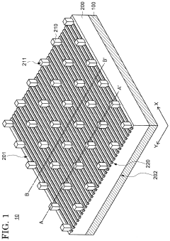
Element transfer device and element transfer method
PatentPendingUS20220262665A1
Innovation
- An element transfer device with an elastic sheet and pickup portions, including a shaft portion and head portions, that can adjust its distance between pickup points to match the spacing on both the element and circuit substrates, allowing for simultaneous transfer of multiple micro LEDs.
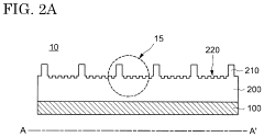
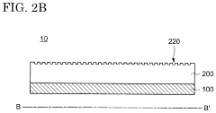
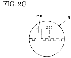
Transfer substrate
PatentPendingUS20220109081A1
Innovation
- A transfer substrate with projection portions and groove portions on its surface, where the groove portions have varying depths and shapes to minimize contact area with the micro LEDs, preventing re-pickup and enhancing the transfer process accuracy.
Supply Chain Considerations for Next-Generation Displays
The global display industry is witnessing a significant transformation as OLED and MicroLED technologies compete for market dominance. Supply chain considerations play a crucial role in determining the trajectory of these next-generation display technologies, influencing both their adoption rates and innovation pathways.
For OLED technology, the supply chain has matured considerably over the past decade, with South Korean manufacturers like Samsung and LG Display establishing robust production ecosystems. These companies have developed vertical integration strategies, controlling everything from material synthesis to panel manufacturing. However, the OLED supply chain remains vulnerable to bottlenecks in certain specialized materials, particularly emissive compounds and thin-film encapsulation solutions, which are often sourced from a limited number of suppliers in Japan and Germany.
MicroLED, as an emerging technology, faces more significant supply chain challenges. The production of MicroLED displays requires expertise in semiconductor manufacturing, LED epitaxy, mass transfer processes, and display integration. Currently, no single company possesses comprehensive capabilities across this entire spectrum, necessitating complex partnership networks. The mass transfer of millions of microscopic LEDs remains a critical bottleneck, with companies like Apple, Samsung, and several startups developing proprietary solutions to address this challenge.
Component sourcing represents another key consideration. While OLED relies on organic materials that have established supply channels but face potential scarcity issues for certain rare elements, MicroLED utilizes inorganic materials that are generally more abundant but require more sophisticated processing. The specialized equipment needed for MicroLED manufacturing also presents a supply chain constraint, as only a handful of companies worldwide can produce the precision tools required for micro-scale LED handling.
Regional dynamics further complicate the supply landscape. East Asia dominates the display manufacturing ecosystem, with China rapidly expanding its capabilities in both technologies. This geographic concentration creates potential vulnerabilities to regional disruptions, as evidenced during recent global supply chain crises. Companies are increasingly exploring supply chain diversification strategies, including establishing manufacturing facilities in new regions like India and Vietnam.
Cost structures differ significantly between these technologies, influencing their respective supply chain strategies. OLED manufacturing benefits from economies of scale but struggles with yield issues at larger panel sizes. MicroLED production currently involves higher capital expenditure and more complex assembly processes, though these costs are expected to decrease as manufacturing techniques mature and supply chains become more efficient.
Environmental Impact and Sustainability of Display Technologies
The environmental impact of display technologies has become increasingly significant as consumer electronics proliferate globally. OLED and MicroLED technologies represent divergent approaches to sustainability challenges in the display industry. OLED displays typically consume less power than traditional LCD screens, particularly when displaying darker content, due to their ability to completely turn off individual pixels. This power efficiency translates to reduced carbon emissions over the product lifecycle, especially for mobile devices where battery conservation is paramount.
MicroLED technology, while still emerging, promises even greater energy efficiency than OLED. Initial research indicates potential power consumption reductions of 30-50% compared to OLED displays of similar brightness. This efficiency stems from MicroLED's superior light emission properties and reduced heat generation, which could substantially decrease the environmental footprint of large-format displays and wearable technologies.
Manufacturing processes present contrasting environmental considerations between these technologies. OLED production involves organic compounds and solvents that require careful handling and disposal. The industry has made significant strides in reducing harmful chemicals, with major manufacturers implementing closed-loop systems that recapture and reuse up to 90% of solvents used in production.
MicroLED manufacturing currently demands more energy-intensive processes, particularly in the precise placement of millions of microscopic LEDs. However, the technology's longer theoretical lifespan—potentially exceeding 100,000 hours compared to OLED's 30,000-50,000 hours—may offset initial production impacts through reduced replacement frequency and electronic waste generation.
End-of-life considerations reveal further distinctions. OLED panels contain trace amounts of heavy metals and organic compounds that present recycling challenges. Industry leaders have established take-back programs, but recovery rates remain below 20% globally. MicroLED displays contain valuable semiconductor materials that may prove more economically viable to recover, potentially driving higher recycling rates once the technology achieves mainstream adoption.
Water usage represents another critical environmental factor. OLED manufacturing typically requires 20-30% less water than traditional LCD production, while preliminary data suggests MicroLED fabrication may reduce water requirements by an additional 15-25% through advanced semiconductor processing techniques that minimize cleaning cycles.
As display technologies evolve, manufacturers are increasingly incorporating sustainability metrics into their innovation roadmaps. Both OLED and MicroLED development teams are exploring biodegradable substrates, reduced rare earth element usage, and modular design approaches that could revolutionize the environmental profile of next-generation displays.
Unlock deeper insights with Patsnap Eureka Quick Research — get a full tech report to explore trends and direct your research. Try now!
Generate Your Research Report Instantly with AI Agent
Supercharge your innovation with Patsnap Eureka AI Agent Platform!