

OLED vs MicroLED: High-Performance Material Advances
OCT 24, 20259 MIN READ
Generate Your Research Report Instantly with AI Agent
Patsnap Eureka helps you evaluate technical feasibility & market potential.
Display Technology Evolution and Objectives
Display technology has undergone remarkable evolution since the introduction of cathode ray tubes (CRTs) in the early 20th century. The progression from CRTs to liquid crystal displays (LCDs) marked the first major shift toward flatter, more energy-efficient screens. This transition was followed by the development of plasma display panels, which offered improved contrast ratios and viewing angles but suffered from high power consumption and screen burn-in issues.
The introduction of Organic Light-Emitting Diode (OLED) technology in the late 1990s represented a paradigm shift in display technology. Unlike LCDs that require backlighting, OLED pixels emit light independently when electrical current passes through organic compounds. This self-emissive property enables perfect blacks, infinite contrast ratios, and thinner form factors, making OLEDs particularly suitable for mobile devices and premium televisions.
Despite OLED's advantages, the technology faces challenges including limited brightness, color degradation over time (particularly with blue OLEDs), and manufacturing complexities that impact yield rates and production costs. These limitations have driven research into alternative display technologies, with MicroLED emerging as a promising contender.
MicroLED technology utilizes microscopic inorganic LED arrays that, like OLEDs, are self-emissive but offer significant improvements in brightness, longevity, and energy efficiency. Each pixel in a MicroLED display consists of red, green, and blue microscopic LEDs measuring less than 100 micrometers, enabling higher pixel density and superior image quality compared to conventional displays.
The current technological battleground between OLED and MicroLED centers on material science advancements. For OLEDs, research focuses on developing more stable blue emitters, improving quantum efficiency, and creating solution-processable materials that can reduce manufacturing costs. Phosphorescent and thermally activated delayed fluorescence (TADF) materials represent significant breakthroughs in enhancing OLED efficiency and lifespan.
For MicroLEDs, material innovation targets improved epitaxial growth processes for gallium nitride (GaN) LEDs, development of more efficient quantum dot color conversion layers, and novel transfer techniques to enable mass production. The miniaturization of LED chips while maintaining high efficiency presents a formidable challenge that requires interdisciplinary approaches combining semiconductor physics, materials science, and precision engineering.
The ultimate objective of current display technology research is to develop solutions that combine the best attributes of both technologies: the perfect blacks and flexibility of OLEDs with the brightness, longevity, and efficiency of MicroLEDs. This pursuit drives exploration of hybrid approaches and entirely new material systems that could potentially transcend the limitations of current display technologies.
Market Demand Analysis for Advanced Display Technologies
The display technology market is experiencing a significant shift as advanced technologies like OLED and MicroLED continue to evolve. Current market analysis indicates that the global advanced display market reached approximately $143 billion in 2022, with projections suggesting growth to $218 billion by 2027, representing a compound annual growth rate of 8.9%. This growth is primarily driven by increasing consumer demand for higher resolution, better color accuracy, and energy efficiency in display technologies.
Consumer electronics remains the dominant application sector, accounting for nearly 65% of the advanced display market. Within this segment, smartphones represent the largest share at 38%, followed by televisions at 27% and wearable devices at 15%. The automotive industry is emerging as a rapidly growing sector for advanced displays, with an estimated growth rate of 12.3% annually as vehicle manufacturers integrate more sophisticated dashboard and entertainment systems.
Regional analysis reveals that Asia-Pacific dominates the manufacturing landscape, with South Korea, Japan, and China collectively accounting for over 70% of global production capacity. However, North America and Europe lead in research and development investments, particularly in next-generation materials for both OLED and MicroLED technologies.
Market research indicates shifting consumer preferences toward displays with higher brightness, better energy efficiency, and longer lifespans. OLED currently holds approximately 58% of the premium display market, while MicroLED is gaining traction in specialized applications requiring extreme brightness and durability. Consumer surveys indicate that 73% of high-end device purchasers consider display quality a critical factor in their buying decisions.
The enterprise and professional markets show increasing demand for advanced display technologies in specialized fields such as medical imaging, design, and simulation. These sectors prioritize color accuracy, resolution, and refresh rates over other factors, creating distinct market segments with specific technical requirements.
Supply chain analysis reveals growing concerns about material sourcing for both technologies. OLED production relies heavily on specific organic compounds with limited suppliers, while MicroLED faces challenges in securing rare earth elements and specialized semiconductor materials. This has prompted major manufacturers to invest in alternative materials research and vertical integration strategies to secure supply chains.
Market forecasts suggest that while OLED will maintain dominance in the near term, MicroLED is expected to capture up to 25% of the premium display market by 2030 as manufacturing costs decrease and material advances improve yield rates. This transition will likely be accelerated by breakthroughs in high-performance materials that address current limitations in both technologies.
OLED vs MicroLED: Current Technical Challenges
Despite significant advancements in display technologies, both OLED and MicroLED face substantial technical challenges that limit their widespread adoption and performance optimization. OLED technology continues to struggle with limited operational lifespan, particularly for blue emitters which typically degrade faster than red and green counterparts. This differential aging leads to color shift over time, compromising display quality and consistency.
Material stability remains a critical issue for OLED displays, with organic compounds being susceptible to oxidation and moisture damage, necessitating complex encapsulation solutions that add to manufacturing complexity and cost. Additionally, OLED efficiency plateaus present barriers to reducing power consumption, especially important for battery-powered devices.
For MicroLED technology, the primary challenge lies in the mass transfer process - efficiently and precisely positioning millions of microscopic LED chips onto display substrates. Current yield rates in this process significantly impact production costs, with even small defect rates translating to substantial waste in high-resolution displays.
MicroLED also faces challenges in achieving uniform performance across differently colored LEDs. Red, green, and blue MicroLEDs exhibit varying efficiency levels and degradation rates, complicating the engineering of balanced, long-lasting displays. The miniaturization of LED chips introduces quantum efficiency droop effects, where smaller LEDs experience reduced light output efficiency.
Both technologies encounter difficulties in flexible display applications. OLED's organic materials are inherently more flexible but suffer from mechanical stress-induced degradation during repeated bending. MicroLED implementations on flexible substrates face challenges with interconnect reliability and maintaining precise alignment during flexing operations.
Heat management represents another shared challenge. OLED displays experience accelerated degradation at higher temperatures, while MicroLED displays generate significant heat that must be efficiently dissipated to maintain performance and longevity. This thermal management becomes increasingly complex as pixel densities increase.
Manufacturing scalability differs between the technologies. OLED benefits from established vapor deposition processes but struggles with consistent quality at larger screen sizes. MicroLED manufacturing lacks standardized, cost-effective mass production techniques, particularly for consumer electronics applications where price sensitivity is high.
Resolution limitations also differ: OLED faces challenges in achieving ultra-high pixel densities due to limitations in patterning organic materials at microscopic scales, while MicroLED struggles with efficient production of sub-10 micrometer LED chips needed for high-resolution displays in compact form factors.
Current High-Performance Material Solutions
01 Organic materials for OLED displays
Organic light-emitting materials are essential components in OLED display technology. These materials include various organic compounds that emit light when an electric current is applied. High-performance organic materials can improve efficiency, color accuracy, and longevity of OLED displays. Advanced formulations of these materials can enhance brightness, reduce power consumption, and extend the operational lifetime of OLED displays.- Organic materials for OLED displays: Organic light-emitting materials are crucial components in OLED display technology. These materials include various organic compounds that emit light when an electric current is applied. High-performance organic materials can improve efficiency, color accuracy, and lifespan of OLED displays. Advanced formulations may include phosphorescent or thermally activated delayed fluorescence (TADF) emitters to enhance quantum efficiency and reduce power consumption.
- MicroLED fabrication and materials: MicroLED display technology utilizes microscopic LED arrays that offer advantages in brightness, energy efficiency, and longevity. The fabrication of these tiny LEDs involves specialized materials and processes to achieve high pixel density and performance. Key materials include semiconductor compounds like gallium nitride (GaN) and indium gallium nitride (InGaN) that enable efficient light emission at various wavelengths. Advanced manufacturing techniques are employed to transfer and bond these micro-scale components onto display substrates.
- Quantum dot enhancement layers: Quantum dot materials can significantly enhance the performance of both OLED and MicroLED displays. These nanoscale semiconductor particles convert light to specific wavelengths with high efficiency, resulting in improved color gamut and brightness. When incorporated as enhancement layers, quantum dots can optimize the spectral output of displays, providing more vivid and accurate colors. The size-dependent emission properties of quantum dots allow for precise color tuning without additional color filters, reducing energy loss.
- Electrode and conductive materials: High-performance electrode and conductive materials are essential for efficient operation of OLED and MicroLED displays. These materials include transparent conductive oxides, metal nanowires, and composite conductors that balance optical transparency with electrical conductivity. Advanced electrode materials enable better current distribution, reduced resistance, and improved light extraction. Innovations in this area focus on flexible, stretchable, and ultra-thin conductive materials that maintain performance while enabling new form factors for displays.
- Encapsulation and barrier materials: Protective encapsulation and barrier materials are critical for extending the lifespan of OLED and MicroLED displays by preventing moisture and oxygen degradation. These high-performance materials include multi-layer thin film encapsulations, hybrid organic-inorganic composites, and specialized adhesives. Advanced barrier films with extremely low water vapor transmission rates protect sensitive organic and inorganic components from environmental factors. Innovations in this area focus on flexible, transparent barriers that maintain protection while enabling bendable and foldable display applications.
02 MicroLED semiconductor materials and structures
MicroLED displays utilize inorganic semiconductor materials to create extremely small light-emitting diodes. These materials, typically based on gallium nitride (GaN) or other III-V semiconductors, enable high brightness, excellent energy efficiency, and superior color performance. Advanced semiconductor structures, including quantum wells and specialized epitaxial layers, are developed to enhance the performance of MicroLED displays, resulting in improved brightness, efficiency, and color gamut.Expand Specific Solutions03 Electrode and conductive materials
High-performance electrode and conductive materials are crucial for both OLED and MicroLED displays. These materials include transparent conductive oxides, metal nanowires, and composite electrodes that provide electrical connectivity while maintaining optical transparency. Advanced electrode materials can improve current distribution, reduce resistance, enhance light extraction, and contribute to the overall efficiency and performance of display devices.Expand Specific Solutions04 Quantum dot materials for display enhancement
Quantum dot materials are increasingly being incorporated into both OLED and MicroLED display technologies to enhance color performance. These nanoscale semiconductor particles can convert light from one wavelength to another with high efficiency, enabling wider color gamuts and improved color accuracy. Integration of quantum dots with display technologies allows for more vibrant colors, better energy efficiency, and enhanced visual performance.Expand Specific Solutions05 Encapsulation and barrier materials
Protective encapsulation and barrier materials are essential for ensuring the longevity and reliability of OLED and MicroLED displays. These materials protect sensitive organic and inorganic components from moisture, oxygen, and other environmental factors that can degrade performance. Advanced barrier films, sealants, and encapsulation technologies can significantly extend the operational lifetime of displays while maintaining flexibility for next-generation form factors.Expand Specific Solutions
Key Industry Players and Competitive Landscape
The OLED vs MicroLED display technology landscape is currently in a transitional phase, with OLED being mature and commercially established while MicroLED remains in early commercialization. The global high-performance display materials market is projected to reach $25-30 billion by 2025, driven by increasing demand for premium displays. Leading companies like Samsung Electronics, LG Display, and BOE Technology have established strong positions in OLED, while Universal Display Corporation dominates OLED materials development. For MicroLED, companies including Apple, Samsung, and eLux are making significant advances, with Applied Materials and Lumileds developing critical manufacturing processes. Academic institutions like Northwestern University and The University of Hong Kong are contributing breakthrough research in novel materials that could accelerate both technologies' evolution.
BOE Technology Group Co., Ltd.
Technical Solution: BOE has made substantial investments in both OLED and MicroLED material technologies. For OLED, BOE has developed a hybrid emitting layer structure combining fluorescent blue with phosphorescent red and green materials, achieving external quantum efficiencies exceeding 25% for green emission. Their proprietary soluble OLED materials enable inkjet-printed displays with reduced material waste of approximately 90% compared to vacuum deposition methods. BOE's recent advances include thermally activated delayed fluorescence (TADF) emitters that achieve nearly 100% internal quantum efficiency without using rare metals. In MicroLED development, BOE has created a novel quantum dot color conversion layer that improves color gamut to over 110% of DCI-P3 while maintaining brightness levels above 1000 nits. Their mass transfer technology utilizes a laser-assisted release process that can transfer over 100,000 MicroLED chips simultaneously with placement accuracy within ±1.5μm. BOE has also developed specialized transparent conductive oxide materials that reduce electrode resistance by 40% while maintaining over 90% transparency for MicroLED applications.
Strengths: Rapidly expanding production capacity for both technologies; strong government backing for R&D; vertical integration from materials to finished displays. Weaknesses: Still catching up to Korean manufacturers in high-end OLED efficiency metrics; MicroLED mass production capabilities not yet fully demonstrated; intellectual property position not as strong as established players.
Samsung Electronics Co., Ltd.
Technical Solution: Samsung has pioneered significant advancements in both OLED and MicroLED technologies. For OLED, Samsung has developed proprietary Quantum Dot OLED (QD-OLED) technology that combines quantum dots with OLED to achieve superior color volume and brightness while maintaining OLED's perfect blacks. Their QD-OLED panels utilize blue OLED as the light source with quantum dot color conversion layers for red and green, eliminating the need for color filters and improving efficiency by approximately 20%. For MicroLED, Samsung has commercialized "The Wall" modular MicroLED display technology featuring inorganic gallium nitride (GaN)-based LEDs with sizes under 50 micrometers. Their latest MicroLED innovations include a mass transfer technique that achieves 99.9% yield in LED placement and a specialized electrode structure that reduces current leakage by 40% while improving luminous efficiency. Samsung has also developed proprietary color conversion materials that enhance the color gamut to over 100% of DCI-P3 for their MicroLED displays.
Strengths: Vertical integration across supply chain from materials to finished displays; proprietary manufacturing processes for both technologies; established mass production capabilities. Weaknesses: High production costs for MicroLED remain a barrier to mainstream adoption; QD-OLED technology still faces challenges with blue OLED material lifetime compared to red and green phosphorescent materials.
Critical Patents in Display Material Science
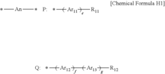
Organic light-emitting diode with high efficiency and long lifetime
PatentActiveUS20170342318A1
Innovation
- The use of specific amine compounds as dopants and anthracene derivatives as hosts in the light-emitting layer, as defined by Chemical Formulas A and H1 to H7, to enhance energy transfer and improve light emission efficiency and longevity.
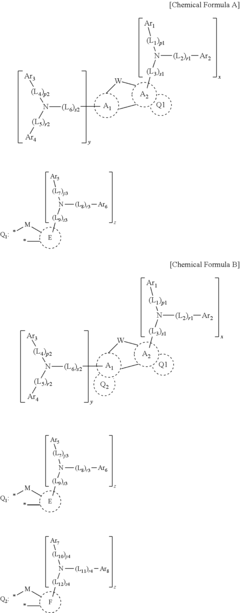
Organic compound, organic light-emitting diode including organic compound, and display device including organic light-emitting diode
PatentActiveUS20220407011A1
Innovation
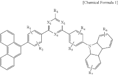
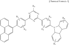
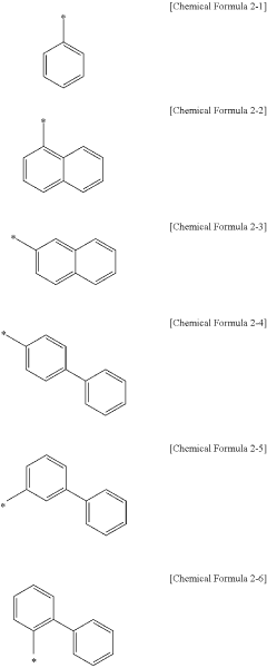
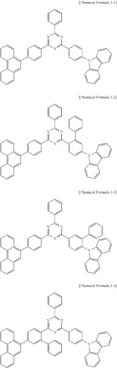
- An organic compound represented by Chemical Formula 1, where X1 to X3 are nitrogen or carbon, and R1 to R7 are selected from hydrogen or substituted aryl/heteroaryl groups, is used as an electron transport material to improve the performance of OLEDs, specifically enhancing electron transport performance and stability.
Supply Chain Considerations for Advanced Display Materials
The supply chain for advanced display materials represents a critical factor in the evolution and market adoption of both OLED and MicroLED technologies. Material sourcing for these advanced displays involves complex global networks that directly impact production costs, manufacturing scalability, and ultimately market competitiveness.
For OLED technology, the supply chain has matured significantly over the past decade, with established procurement channels for organic materials, particularly for red, green, and blue emitters. South Korea and Japan dominate the high-purity OLED material production landscape, with companies like UDC, Idemitsu Kosan, and Dow Chemical controlling significant intellectual property. This geographical concentration creates potential vulnerabilities, as evidenced during recent global supply chain disruptions.
MicroLED supply chains, by contrast, remain in nascent development stages with considerable fragmentation. The technology requires specialized semiconductor materials, particularly gallium nitride (GaN) for blue and green emitters, and aluminum gallium indium phosphide (AlGaInP) for red emitters. These materials face more severe supply constraints, with limited production capacity concentrated primarily in Taiwan, Japan, and Germany.
Both technologies face critical rare earth element dependencies. OLED production relies on indium, which faces potential supply constraints due to limited global reserves and geopolitical factors affecting mining regions. MicroLED manufacturing depends on gallium and rare earth phosphors, which present similar supply security challenges. These material constraints represent significant barriers to production scaling and cost reduction.
Manufacturing equipment represents another crucial supply chain consideration. OLED production relies on specialized vacuum deposition systems primarily sourced from South Korean and Japanese manufacturers. MicroLED requires advanced semiconductor manufacturing equipment and specialized transfer technologies, with a more diverse but less mature supplier ecosystem spanning North America, Europe, and East Asia.
Recycling infrastructure development presents divergent challenges for these technologies. OLED materials pose environmental concerns due to their organic composition, while MicroLED components contain valuable semiconductor materials that could potentially support circular economy initiatives if appropriate recovery systems are established.
The resilience of these supply chains will significantly influence technology adoption timelines. OLED benefits from established supplier relationships and production infrastructure, while MicroLED faces greater uncertainty with emerging supplier networks. Companies investing in either technology must carefully evaluate supply chain risks, including geopolitical factors, material availability projections, and supplier diversification opportunities to ensure sustainable production capabilities.
Environmental Impact and Sustainability Factors
The environmental footprint of display technologies has become increasingly important as sustainability concerns rise globally. OLED and MicroLED technologies present distinct environmental profiles throughout their lifecycles, from raw material extraction to end-of-life disposal.
OLED manufacturing processes typically involve organic compounds that require fewer rare earth elements compared to traditional LED technologies. However, these processes often utilize solvents and chemicals that can be environmentally problematic if not properly managed. Recent advances in water-based OLED manufacturing techniques have shown promise in reducing harmful chemical usage by up to 35%, significantly decreasing the environmental impact of production.
MicroLED technology, while offering exceptional energy efficiency during operation, presents challenges in manufacturing sustainability. The production process requires precise placement of millions of microscopic LEDs, often utilizing energy-intensive processes and specialized equipment. Current manufacturing methods generate approximately 30% more electronic waste during production compared to OLED manufacturing, primarily due to yield issues in the early stages of technology development.
Energy consumption during device operation represents a critical sustainability factor. MicroLED displays demonstrate superior energy efficiency, consuming approximately 50% less power than comparable OLED displays at equivalent brightness levels. This efficiency advantage becomes particularly significant in large-format displays and could potentially reduce global display energy consumption by billions of kilowatt-hours annually if widely adopted.
End-of-life considerations reveal further distinctions between these technologies. OLED panels contain organic materials that can degrade more naturally than inorganic components, though the presence of heavy metals in some formulations remains problematic. MicroLED displays contain higher concentrations of gallium, indium, and other elements that present recycling challenges but are potentially more recoverable in concentrated form.
Water usage presents another environmental consideration. Traditional OLED manufacturing processes consume approximately 45-60 liters of ultra-pure water per square meter of display produced. Recent material advances have reduced this requirement by implementing closed-loop water recycling systems, achieving up to 70% water reuse in advanced facilities. MicroLED manufacturing currently requires approximately 25% more water usage, though this gap is narrowing with process refinements.
Carbon footprint analyses indicate that while MicroLED manufacturing currently generates higher emissions during production, the lifetime carbon impact may be lower due to extended operational lifespan and reduced energy consumption. Material innovations focusing on bio-based substrates and environmentally benign semiconductors show promise for both technologies, potentially reducing their environmental impact by 40-60% in the next generation of displays.
Unlock deeper insights with Patsnap Eureka Quick Research — get a full tech report to explore trends and direct your research. Try now!
Generate Your Research Report Instantly with AI Agent
Supercharge your innovation with Patsnap Eureka AI Agent Platform!